

Dual 3 MHz, 600 mA Buck
FEATURES
Input voltage range: 2.4 V to 5.5 V
Tiny 16-ball, 2 mm × 2 mm WLCSP package
Overcurrent and thermal protection
Soft start
Factory programmable undervoltage lockout on VDDA
system supply of either 2.2 V or 3.9 V
Factory programmable default output voltages for all
3 channels
Buck1 and Buck2 key specifications
Current mode architecture for excellent transient response
3 MHz operating frequency
Uses tiny multilayer inductors and capacitors
Forced PWM and auto PWM/PSM modes
Out-of-phase operation for reduced input filtering
100% duty cycle low dropout mode
24 μA typical quiescent current per channel, no switching
LDO key specifications
Stable with 1 μF ceramic output capacitors
High PSRR
60 dB up to 10 KHz
Low output noise
65 μV rms output noise at VOUT3 = 3.3 V
Low dropout voltage: 150 mV @ 150 mA load
11 μA typical ground current at no load
APPLICATIONS
USB devices
Handheld products
Multivoltage power for processors, ASICS, FPGAs,
and RF chipsets
Regulator with 150 mA LDO
ADP5022
GENERAL DESCRIPTION
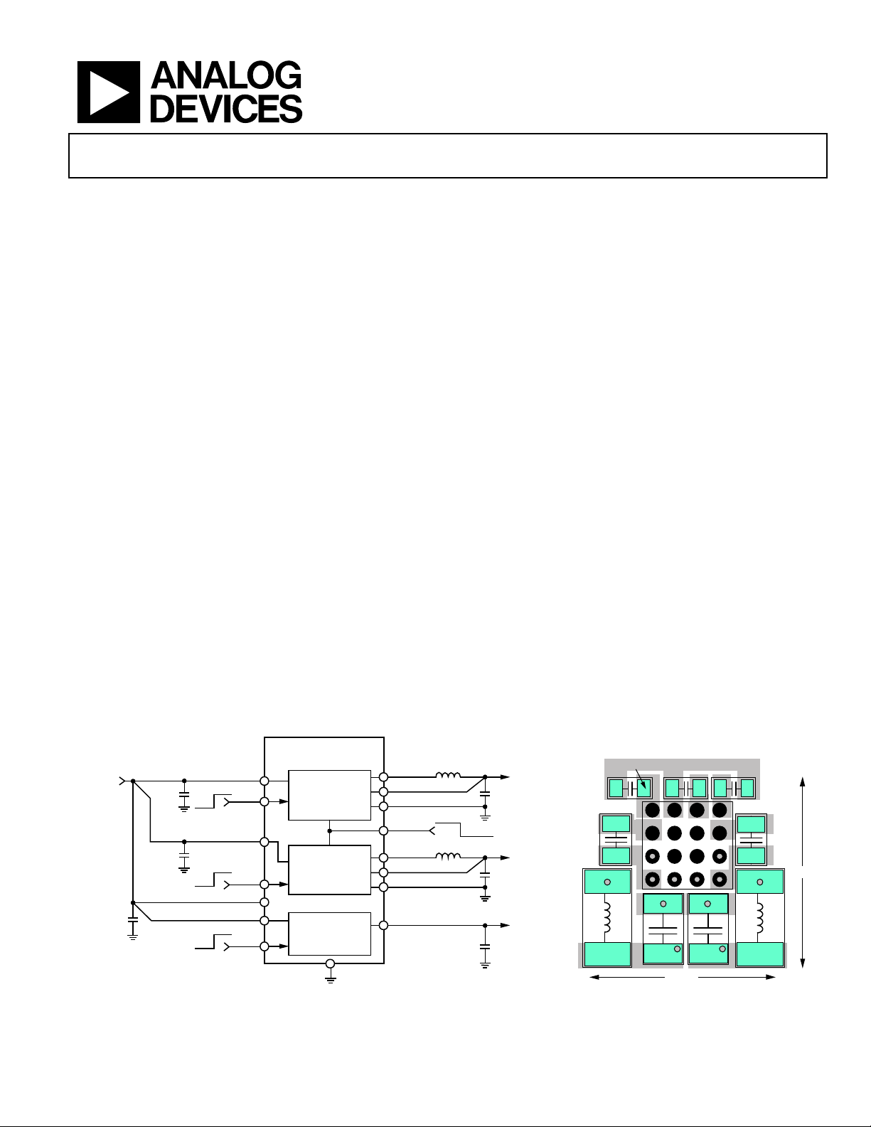
The ADP5022 is a micro power management unit (micro PMU)
that combines two high performance buck regulators and a low
dropout regulator (LDO) in a tiny 16-ball 2.08 mm × 2.08 mm
WLCSP to meet demanding performance and board space
requirements.
The high switching frequency of the buck regulators enables
tiny multilayer external components and minimizes the board
space required. When the MODE pin is set high, the buck regulators operate in forced PWM mode. When the MODE pin is
set low, the buck regulators automatically switch operating
modes, depending on the load current level. At higher output
loads, the buck regulators operate in PWM mode. When the
load current falls below a predefined threshold, the regulators
operate in power save mode (PSM), improving the light-load
efficiency.
The two bucks operate out-of-phase to reduce the input
capacitor requirement and noise.
The low quiescent current, low dropout voltage, and wide input
voltage range of the ADP5022 LDO extends the battery life of
portable devices. The LDO maintains power supply rejection
greater than 60 dB for frequencies as high as 10 kHz while
operating with a low headroom voltage.
Each regulator in the ADP5022 has a dedicated, independent
enable pin. A high voltage level applied to the enable pin activates
the respective regulator. The default output voltages are factory
programmable and can be set to a wide range of options.
ADP5022
VIN = 2.4V
TO 5.5V
1µF
VIN1
OFF
OFF
OFF
ON
ON
ON
EN1
VIN2
EN2
VDDA
VIN3
EN3
C2
4.7µF
C3
4.7µF
C1
BUCK1
EN_BK1
MODE
MODE
BUCK2
EN_BK2
LDO1
EN_LDO1
AGND
SW1
VOUT1
PGND1
MODE
SW2
VOUT2
PGND2
VOUT3
Figure 1. Typical Applications Circuit Figure 2. Typical PCB Layout
Rev. B
Information furnished by Analog Devices is believed to be accurate and reliable. However, no
responsibility is assumed by Analog Devices for its use, nor for any infringements of patents or other
rights of third parties that may result from its use. Specifications subject to change without notice. No
license is granted by implication or otherwise under any patent or patent rights of Analog Devices.
Trademarks and registered trademarks are the property of their respective owners.
L1
1µH
PWM
L2
1µH
PWM/PSM
V
@
OUT1
600mA
C4
10µF
V
@
OUT2
600mA
C5
10µF
V
@
OUT3
150mA
C6
1µF
08253-001
One Technology Way, P.O. Box 9106, Norwood, MA 02062-9106, U.S.A.
Tel: 781.329.4700 www.analog.com
Fax: 781.461.3113 ©2009–2010 Analog Devices, Inc. All rights reserved.
C1
L1
COUT_3
C4C3
INDUCTOR
COUT_1 COUT_2
4.7mm
C2
5.0mm
INDUCTOR
08253-061

ADP5022
TABLE OF CONTENTS
Features .............................................................................................. 1
Applications ....................................................................................... 1
General Description ......................................................................... 1
Revision History ............................................................................... 2
Specifications ..................................................................................... 3
Buck1 and Buck2 Specifications ................................................. 4
LDO Specifications ...................................................................... 5
Absolute Maximum Ratings ............................................................ 6
Thermal Data ................................................................................ 6
Thermal Resistance ...................................................................... 6
ESD Caution .................................................................................. 6
Pin Configuration and Function Descriptions ............................. 7
Typical Performance Characteristics ............................................. 8
REVISION HISTORY
6/10—Rev. A to Rev. B
Changes to Ordering Guide .......................................................... 25
11/09—Revision A: Initial Version
Theory of Operation ...................................................................... 16
Power Management Unit ........................................................... 16
Buck Section ................................................................................ 17
LDO Section ............................................................................... 18
Applications Information .............................................................. 19
Buck External Component Selection ....................................... 19
LDO Capacitor Selection .......................................................... 20
PCB Layout Guidelines .................................................................. 22
Evaluation Board schematics and Artwork ................................ 23
Suggested Layout ........................................................................ 23
Outline Dimensions ....................................................................... 25
Ordering Guide .......................................................................... 25
Rev. B | Page 2 of 28

ADP5022
SPECIFICATIONS
VDDA = VIN1 = VIN2 = 3.6 V, VIN3 = (VOUT3 + 0.5 V) or 2.4 V, whichever is greater, VIN3 ≤ VIN1, TJ = −40°C to +125°C, unless
otherwise noted.
Table 1.
Parameter Symbol Test Conditions/Comments Min Typ Max Unit
INPUT VOLTAGE RANGE
System and Buck Input Supplies Voltage Range
High UVLO level models 4.5 5.5 V
LDO Input Supply Voltage Range V
SHUTDOWN CURRENT
I
THERMAL SHUTDOWN
Thermal Shutdown Threshold TSDTH T
Thermal Shutdown Hysteresis TSD
EN1, EN2, EN3, MODE INPUTS
EN1, EN2, EN3, MODE Input Logic High VIH VDDA = VIN1 = VIN2 1.2 V
EN1, EN2, EN3, MODE Input Logic Low VIL VDDA = VIN1 = VIN2 0.4 V
EN1, EN2, EN3, MODE Input Leakage Current V
STANDBY CURRENT
All Channels Enabled, No Load I
All Channels Enabled, No Load, No Buck Switching I
VIN3 UNDERVOLTAGE LOCKOUT
Input Voltage Rising UVLO
Input Voltage Falling UVLO
VDDA UNDERVOLTAGE LOCKOUT
Input Voltage Rising UVLO
Low UVLO level (factory programmed) 2.35 V
Input Voltage Falling UVLO
Low UVLO level (factory programmed) 2.00 V
1
All limits at temperature extremes are guaranteed via correlation using standard statistical quality control.
1
, V
V
DDA
IN1
and V
IN2
2.3 5.5 V
IN3
EN1 = EN2 = EN3 = GND 0.5 µA
GND-SD
20 °C
HYS
Pin at (VDDA = VIN1 = VIN2) or GND 0.05 1 µA
I-LEAKAGE
80 µA
STBY
59 85 µA
STBY-NOSW
VIN3RISE
VIN3FALL
VDDARISE
VDDAFALL
Low UVLO level models 2.4 5.5 V
,
EN1 = EN2 = EN3 = GND
= −40°C to +85°C
T
J
rising 150 °C
J
2 µA
2.20 V
1.45 V
High UVLO level (factory programmed) 4.15 V
High UVLO level (factory programmed) 3.40 V
Rev. B | Page 3 of 28

ADP5022
BUCK1 AND BUCK2 SPECIFICATIONS
VDDA = VIN1 = VIN2 = 3.6 V, VIN3 = (VOUT3 + 0.5 V) or 2.4 V, whichever is greater, VIN3 ≤ VIN1, TJ = −40°C to +125°C, unless
otherwise noted.
Table 2.
Parameter Symbol Test Conditions/Comments Min Typ Max Unit
OPERATING SUPPLY CURRENT
Buck1 Only I
Buck2 Only I
Buck1 and Buck2 Only I
OUTPUT VOLTAGE ACCURACY V
POWER SAVE MODE TO PWM CURRENT
THRESHOLD
PWM TO POWER SAVE MODE CURRENT
THRESHOLD
SW CHARACTERISTICS, BUCK1 and BUCK2
PFET On Resistance R
Typical at VIN1 = VIN2 = 5.0 V 125 mΩ
NFET On Resistance R
Typical at VIN1 = VIN2 = 5.0 V 100 mΩ
Current Limit I
OSCILLATOR FREQUENCY FSW 2.5 3.0 3.5 MHz
START-UP TIME2
From Shutdown State T
1
All limits at temperature extremes are guaranteed via correlation using standard statistical quality control.
2
Start-up time is defined as the time from a rising edge on EN1/EN2 to VOUT1/VOUT2 reaching 90% of their nominal value.
1
GND1
= 0 mA, device not switching, EN1
I
LOAD 1
24 A
= VDDA, EN2 = EN3 = GND
GND2
= 0 mA, device not switching, EN2
I
LOAD 2
32 A
= VDDA, EN1 = EN3 = GND
GND1-2
I
LOAD 1
= I
= 0 mA, device not switch-
LOAD 1
48 64 A
ing, EN1 = EN2 = VDDA, EN3 = GND
, V
OUT1
I
PSM-PWM
I
PWM-PSM
PFET
NFET
LIMIT1
STARTUP12-SD
OUT2
PWM mode, VIN1 = VIN2 = 2.4 V to 5.5 V,
= I
I
LOAD 1
= 0 mA − 600 mA
LOAD 2
−3 +3 %
105 mA
100 mA
Typical at VIN1 = VIN2 = 3.6 V 165 275 mΩ
Typical at VIN1 = VIN2 = 3.6 V 125 220 mΩ
, I
PFET switch peak current limit 750 950 1050 mA
LIMIT2
250 s
Rev. B | Page 4 of 28

ADP5022
LDO SPECIFICATIONS
VDDA = VIN1 = VIN2 = 3.6 V, VIN3 = (VOUT3 + 0.5 V) or 2.3 V, whichever is greater, VIN3 ≤ VIN1, I
1 µF, T
= −40°C to +125°C, unless otherwise noted.1
J
Table 3.
Parameter Symbol Test Conditions/Comments Min Typ Max Unit
OPERATING SUPPLY CURRENT2 I
I
I
I
OUTPUT VOLTAGE ACCURACY V
VIN3-GND
= 0 µA 11 21 µA
OUT3
= 10 mA 16 29 µA
OUT3
= 150 mA 31 43 µA
OUT3
OUT3
100 µA < I
< 150 mA,
OUT3
VIN3 = (VOUT3 + 0.5 V) to 5.5 V
REGULATION
Line Regulation VOUT3/V
Load Regulation3 VOUT3/I
VIN3 = (VOUT3 + 0.5 V) to 5.5 V, I
IN3
I
OUT3
= 1 mA to 150 mA 0.002 0.0075 %/mA
OUT3
= 1 mA −0.03 +0.03 %/ V
OUT
DROPOUT VOLTAGE4
V
VOUT3 = 3.0 V, I
VOUT3 = 3.0 V, I
DROPOUT
= 10 mA 7 mV
OUT3
= 150 mA 110 150 mV
OUT3
START-UP TIME5
From Shutdown State T
CURRENT-LIMIT THRESHOLD6 I
STARTUP3-SD
LIMIT3
OUTPUT NOISE OUT
200 µs
160 240 350 mA
NOISE
10 Hz to 100 kHz, VIN3 = 5 V, VOUT3 = 3.3 V 65 µV rms
10 Hz to 100 kHz, VIN3= 5 V, VOUT3 = 2.4 V 52 µV rms
10 Hz to 100 kHz, VIN3 = 5 V, VOUT3 = 1.2 V 40 µV rms
POWER SUPPLY REJECTION RATIO PSRR
10 kHz, VIN3 = 5 V, VOUT3 = 3.3 V 60 dB
10 kHz, VIN3 = 5 V, VOUT3 = 2.3 V 66 dB
10 kHz, VIN3 = 5 V, VOUT3 = 1.2 V 70 dB
1
All limits at temperature extremes are guaranteed via correlation using standard statistical quality control.
2
LDO operating supply current is the current drawn from VIN3 to AGND when the LDO is enabled. Whenever any regulator channel is enabled, current is drawn from
VIN1 to AGND. This current is 8 µA typical and is included in the I
3
Based on an end-point calculation using 1 mA and 150 mA loads.
4
Dropout voltage is defined as the input-to-output voltage differential when the input voltage is set to the nominal output voltage. This applies only for output
voltages above 2.3 V.
5
Start-up time is defined as the time between the rising edge of EN3 to VOUT3 being at 90% of its nominal value.
6
Current-limit threshold is defined as the current at which VOUT3 drops to 90% of the specified typical value. For example, the current limit for a 3.0 V output voltage is
defined as the current that causes the output voltage to drop to 90% of 3.0 V or 2.7 V.
GND1
, I
GND2
, and I
specifications.
GND1-2
= 10 mA; C
OUT3
IN3
= C
OUT3
=
−2 +2 %
Rev. B | Page 5 of 28
ADP5022
ABSOLUTE MAXIMUM RATINGS
of the package is based on modeling and calculation using a
θ
Table 4.
Parameter Rating
VDDA, VIN1, VIN2, VIN3, VOUT1, VOUT2,
VOUT3, EN1, EN2, EN3, MODE to GND
Storage Temperature Range −65°C to +150°C
Operating Junction Temperature Range −40°C to +125°C
Soldering Conditions JEDEC J-STD-020
−0.3 V to +6 V
Stresses above those listed under Absolute Maximum Ratings
may cause permanent damage to the device. This is a stress
rating only; functional operation of the device at these or any
other conditions above those indicated in the operational
section of this specification is not implied. Exposure to absolute
maximum rating conditions for extended periods may affect
device reliability.
THERMAL DATA
Absolute maximum ratings apply individually only, not in
combination.
The ADP5022 can be damaged when the junction temperature
limits are exceeded. Monitoring ambient temperature (T
not guarantee that the junction temperature (T
) is within the
J
specified temperature limits. In applications with high power
dissipation and poor thermal resistance, the maximum ambient
temperature may have to be derated. In applications with
moderate power dissipation and low PCB thermal resistance,
the maximum ambient temperature may exceed the maximum
limit as long as the junction temperature is within specification
limits. T
dissipation (P
thermal resistance (θ
calculated from T
of the device is dependent on TA, the power
J
) of the device, and the junction-to-ambient
D
) of the package. Maximum TJ is
JA
and PD using the following formula:
A
= TA + (PD × θJA)
T
J
) does
A
JA
4-layer board. The junction-to-ambient thermal resistance is
highly dependent on the application and board layout. In
applications where high maximum power dissipation exists,
close attention to thermal board design is required. The value
of θ
may vary, depending on PCB material, layout, and envi-
JA
ronmental conditions. The specified values of θ
are based on a
JA
4-layer, 4” × 3” circuit board. Refer to JEDEC JESD 51-9 for
detailed information on the board construction. For additional
information, see the AN-617 Application Note, MicroCSP
TM
Wafer L ev e l Chi p Scal e Pa ck ag e.
THERMAL RESISTANCE
θJA is specified for the worst-case conditions, that is, a device
soldered on a circuit board.
Table 5. Thermal Resistance
Package Type θJA Unit
16-Ball, 0.5 mm Pitch WLCSP 65 °C/W
ESD CAUTION
Rev. B | Page 6 of 28
ADP5022
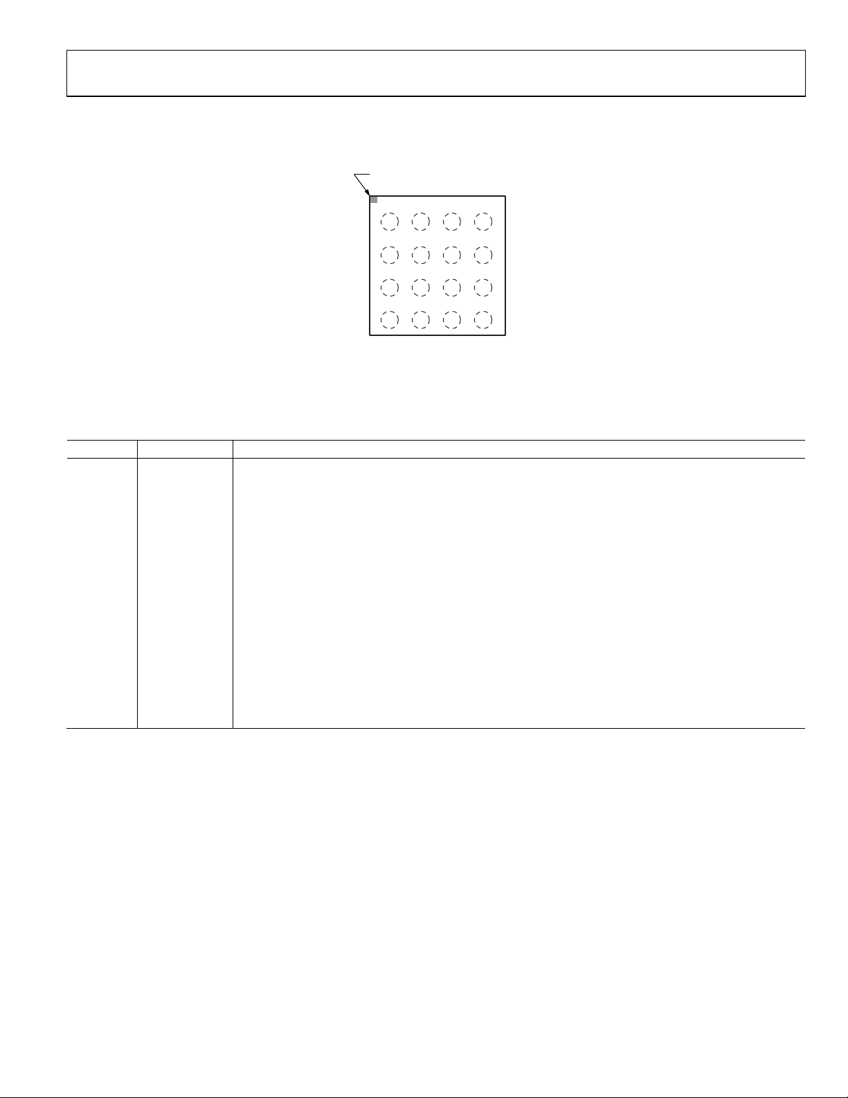
PIN CONFIGURATION AND FUNCTION DESCRIPTIONS
BALLA1
INDICATOR
VOUT3
A
B
C
PGND1
D
Figure 3. Pin Configuration
Table 6. Pin Function Descriptions
Pin No. Mnemonic Description
A1 VOUT3 LDO Output Voltage and Sensing Input.
A2 AGND Analog Ground.
A3 VIN3 LDO Input Supply (VIN3 ≤ VIN1 = VIN2 = VDDA).
A4 VDDA Supply Input for the Housekeeping Block and UVLO Sensing.
B1 VIN1 Buck1 Input Supply (VIN1 = VIN2 = VDDA).
B2 EN1 Buck1 Activation. Set EN1 = high: turn on Buck1. Set EN1 = low: turn off Buck1.
B3 EN2 Buck2 Activation. Set EN2 = high: turn on Buck2. Set EN2 = low: turn off Buck2.
B4 VIN2 Buck2 Input Supply (VIN2 = VIN1 = VDDA).
C1 SW1 Buck1 Switching Node.
C2 EN3 LDO Activation. Set EN3 = high: turn on LDO. EN3 = low: turn off LDO.
C3 MODE Buck1/Buck2 Operating Mode: MODE = high: forced PWM operation. MODE = low: auto PWM/PSM operation.
C4 SW2 Buck2 Switching Node.
D1 PGND1 Dedicated Power Ground for Buck1.
D2 VOUT1 Buck1 Output Voltage Sensing Input.
D3 VOUT2 Buck2 Output Voltage Sensing Input.
D4 PGND2 Dedicated Power Ground for Buck2.
234
1
AGND
VIN1
EN1
SW1
EN3
VOUT1
TOP VIEW
(BALL SIDE DOW N)
Not to Scal e
VIN3
EN2
MODE
VOUT2
VDDA
VIN2
SW2
PGND2
08253-002
Rev. B | Page 7 of 28
ADP5022
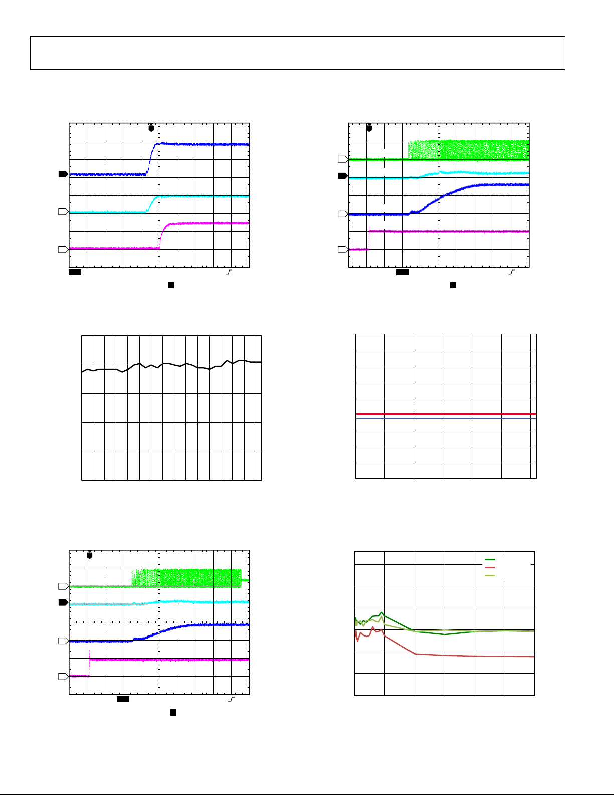
TYPICAL PERFORMANCE CHARACTERISTICS
VIN1 = VIN2 = VIN3 = VDDA = 5.0 V, TA = 25°C, unless otherwise noted.
T
1
2
VOUT1
VOUT2
VOUT3
3
CH1 2.00V M 200µ s A CH1 1.92V
CH3 2.00V
B
W
B
W
CH2 2.00V
B
W
T 45.40%
08253-023
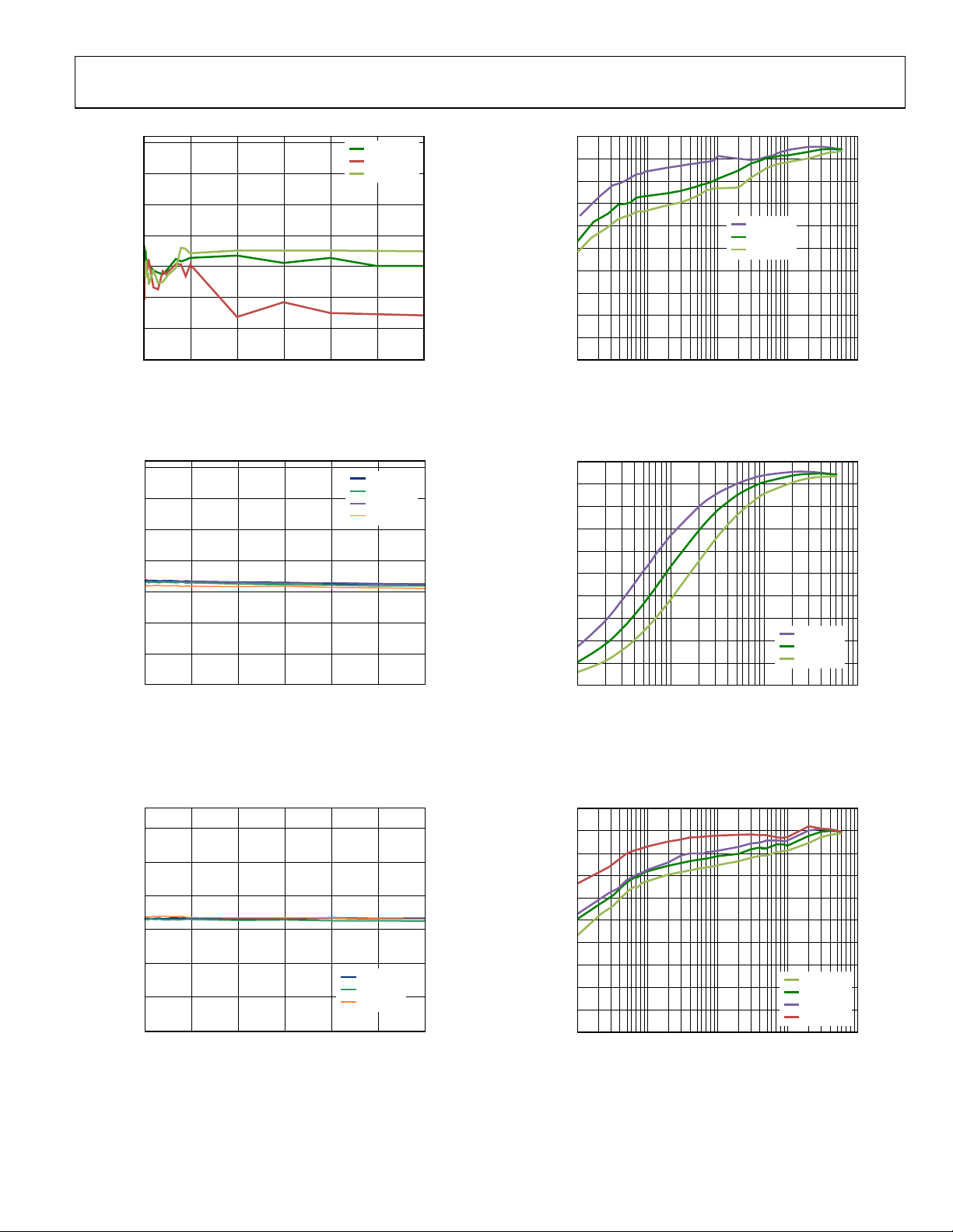
Figure 4. 3-Channel Start-Up Waveforms, VIN3 Cascaded from VOUT1
0.00010
0.00008
0.00006
A (A)
IN
I
0.00004
0.00002
0
2.82.62.4 3.0 3.2 3.4 3.6 3.8 4.0 4.2 4.4 4.6 4.8 5.0 5.2 5.4
(V)
V
IN
Figure 5. System Quiescent Current vs. Input Voltage, VOUT1 = 0.8 V,
VOUT2 = 2.5 V, VIN3 = VOUT2, VOUT3 = 1.2 V, All Channels Unloaded
T
4
2
1
3
CH1 2.00V
CH3 5.00V
SW
VOUT
EN
I
IN
B
CH2 50.0mA Ω
W
B
CH4 5.00V
W
B
M 40.0µs A CH3 2. 2V
W
B
W
T 11.20%
Figure 7. Buck2 Startup, VOUT2 = 1.8 V, I
OUT2
08253-020
= 5 mA
0.15
0.14
0.13
0.12
0.11
0.10
0.09
OUTPUT CURRENT (A)
PSM TO PWM
PWM TO PSM
0.08
0.07
0.06
2.4 2. 9 3. 4 3. 9 4. 4 4.9 5.4
08253-064
INPUT VOLTAGE (V)
08253-067
Figure 8. Buck 2 PSM to PWM Transition, VOUT2 = 1.8 V
T
4
2
1
3
CH1 2.00V
CH3 5.00V
SW
VOUT
EN
I
IN
B
B
W
W
CH2 50.0mA Ω
CH4 5.00V
B
W
B
W
Figure 6. Buck1 Startup, VOUT1 = 3.3 V, I
M 40.0µs A CH3 2.2V
T 11.20%
= 10 mA
OUT1
08253-021
Rev. B | Page 8 of 28
3.354
TA= +25°C
T
= –40°C
A
T
= +85°C
A
3.334
3.314
A (V)
3.294
OUT
V
3.274
3.254
3.234
0 0.1 0.2 0.3 0.4 0.6
I
(A)
OUT
0.5
Figure 9. Buck1 Load Regulation Across Temperature, VOUT1 = 3.3 V,
Auto Mode
08253-058
ADP5022
1.834
1.824
1.814
1.804
B (V)
OUT
1.794
V
1.784
1.774
1.764
0 0.1 0.2 0.3 0.4 0.6
I
OUT
(A)
TA= +25°C
T
= –40°C
A
T
= +85°C
A
0.5
Figure 10. Buck2 Load Regulation Across Temperature, VOUT2 = 1.8 V,
Auto Mode
08253-057
100
90
80
70
(A)
VIN = 3.6V
V
= 4.5V
IN
V
= 5.5V
IN
60
50
40
EFFICIENCY (%)
30
20
10
0
0.0001 0.001 0.01 0.1 1
I
OUT
Figure 13. Buck1 Efficiency vs. Load Current, Across Input Voltage,
VOUT1 = 3.3 V, Auto Mode
08253-038
1.834
1.824
1.814
1.804
B (V)
OUT
V
1.794
1.784
1.774
1.764
0 0.1 0.2 0.3 0.4 0.60.5
I
OUT
(A)
VIN = 5.5V
V
= 4.5V
IN
V
= 3.6V
IN
V
= 2.4V
IN
Figure 11. Buck 2 Load Regulation Across Input Voltage, VOUT1 = 1.8 V,
PWM Mode
3.354
3.334
3.314
A (V)
3.294
OUT
V
3.274
3.254
3.234
0 0.1 0.2 0.3 0.4 0.60.5
I
OUT
(A)
VIN = 3.6V
V
= 4.5V
IN
V
= 5.5V
IN
Figure 12. Buck1 Load Regulation Across Input Voltage, VOUT2 = 3.3 V,
PWM Mode
100
90
80
70
60
50
40
EFFICIENCY (%)
30
20
10
0
08253-054
0.001 0.01 0. 1 1
I
OUT
(A)
VIN = 3.6V
V
= 4.5V
IN
V
= 5.5V
IN
08253-039
Figure 14. Buck1 Efficiency vs. Load Current, Across Input Voltage,
VOUT1 = 3.3 V, PWM Mode
100
90
80
70
60
50
40
EFFICIENCY (%)
30
20
10
0
08253-055
0.0001 0.001 0.01 0.1 1
I
OUT
(A)
VIN = 5.5V
V
= 4.5V
IN
V
= 3.6V
IN
V
= 2.4V
IN
08253-036
Figure 15. Buck2 Efficiency vs. Load Current, Across Input Voltage,
VOUT2 = 1.8 V, Auto Mode
Rev. B | Page 9 of 28
 Loading...