

Power Management Unit
VIN2
V
V
FEATURES
Input voltage range: 2.4 V to 5.5 V
Low standby current: 1 μA
Switching frequency: 3 MHz
2
I
C interface
Synchronous Buck 1 regulator: 600 mA
Synchronous Buck 2 regulator: 250 mA
Low dropout regulator (LDO): 150 mA
Internal compensation
Internal soft start
Thermal shutdown
20-lead 4 mm × 4 mm LFCSP
APPLICATIONS
Digital cameras, handsets
Mobile TVs
for Imaging Modules
ADP5020
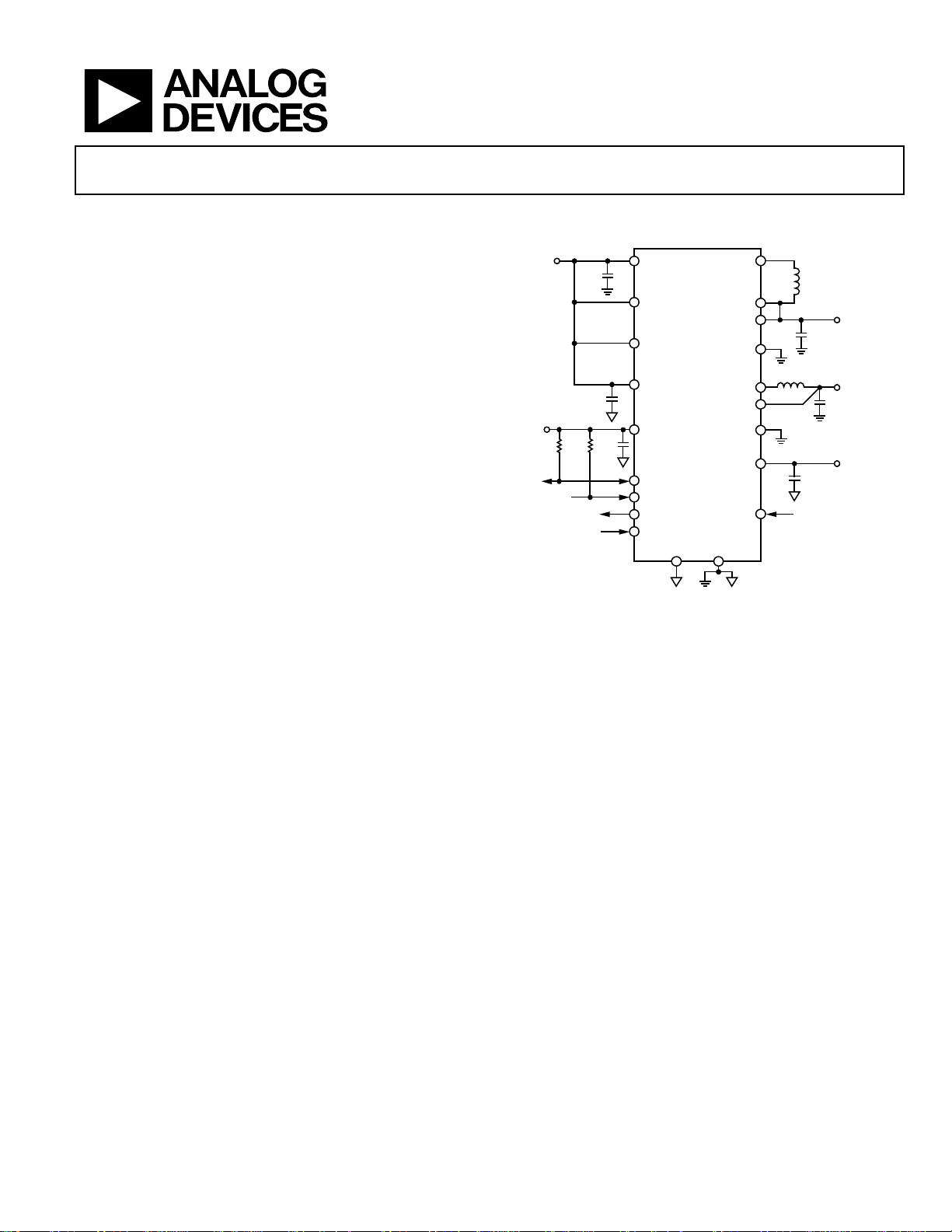
TYPICAL APPLICATIONS CIRCUIT
.4V TO 5.5
V
DD_IO
1.7V TO 3. 6
10kΩ 10kΩ
10µF
VDD1
VDD2
VDD3
ADP5020
VDDA
1µF
VDD_IO
0.1µF
SDA
SCL
XSHTDN
EN/GPIO
DGND AGND
SW1
VOUT1
VOUT1
PGND1
SW2
VOUT2
PGND2
VOUT3
SYNC
2.2µH
EXT. FREQ
9.6/19.2MHz
2.2µH
V
2.5V TO 3. 7V
10µF
V
1.1V TO 1. 8V
4.7µF
V
1.8V TO 3. 3V
1µF
OUT1
OUT2
OUT3
GENERAL DESCRIPTION
The ADP5020 provides a highly integrated power solution that
includes all of the power circuits necessary for a digital imaging
module. It comprises two step-down dc-to-dc converters, one
LDO, and a power sequence controller. All dc-to-dc converters
integrate power pMOSFETs and nMOSFETs, making the system
simpler and more compact and reducing the cost. The ADP5020
has digitally programmed output voltages and buck converters
that can source up to 600 mA. A fixed frequency operation of
3 MHz enables the use of tiny inductors and capacitors. The buck
converters use a voltage mode, constant-frequency PWM control
scheme, and the synchronous rectification is implemented to
reduce the power loss. The Buck 1 regulator operates at up to
93% efficiency.
Figure 1.
The ADP5020 provides high performance, reduces component
count and size, and is lower in cost when compared to conventional designs.
The ADP5020 runs on input voltage from 2.4 V to 5.5 V and
supports one-cell lithium-ion (Li+) batteries. The high performance LDO maximizes noise suppression. The ADP5020 can be
activated via an I
2
C® interface or through a dedicated enable input.
During logic-controlled shutdown, the input is disconnected
from the output source, and the part draws 1 μA typical from
the input source. Other key features include undervoltage lockout
to prevent deep-battery discharge and soft start to prevent input
current overshoot at startup. The ADP5020 is available in a
20-lead LFCSP.
07774-001
Rev. 0
Information furnished by Analog Devices is believed to be accurate and reliable. However, no
responsibility is assumed by Analog Devices for its use, nor for any infringements of patents or other
rights of third parties that may result from its use. Specifications subject to change without notice. No
license is granted by implication or otherwise under any patent or patent rights of Analog Devices.
Trademarks and registered trademarks are the property of their respective owners.
One Technology Way, P.O. Box 9106, Norwood, MA 02062-9106, U.S.A.
Tel: 781.329.4700 www.analog.com
Fax: 781.461.3113 ©2009 Analog Devices, Inc. All rights reserved.

ADP5020
TABLE OF CONTENTS
Features .............................................................................................. 1
Applications ....................................................................................... 1
Typical Applications Circuit ............................................................ 1
General Description ......................................................................... 1
Revision History ............................................................................... 2
Functional Block Diagram .............................................................. 3
Specifications ..................................................................................... 4
Switching Specifications .............................................................. 5
DC-to-DC Conversion Specifications, Buck 1 Regulator ....... 5
DC-to-DC Conversion Specifications, Buck 2 Regulator ....... 6
VOUT3 Specifications, Low Dropout (LDO) Regulator ........ 6
I2C Timing Specifications ............................................................ 7
Absolute Maximum Ratings ............................................................ 8
Thermal Resistance ...................................................................... 8
ESD Caution .................................................................................. 8
Pin Configuration and Function Descriptions ............................. 9
Typical Performance Characteristics ........................................... 10
Theory of Operation ...................................................................... 13
Circuit Operation ....................................................................... 13
Internal Compensation .............................................................. 13
Current Limiting and Short-Circuit Protection ..................... 13
Synchronization .......................................................................... 13
I2C Interface ................................................................................ 13
Undervoltage Lockout ............................................................... 13
Thermal Shutdown .................................................................... 13
Control Registers ............................................................................ 14
Device Address ........................................................................... 14
Register Map ............................................................................... 14
Register Descriptions ................................................................. 14
Power-Up/Power-Down Sequence ............................................... 17
Sequencer .................................................................................... 17
Default Power-On Sequence with EN Pin .............................. 17
Power-On Sequence Using the I2C Interface .............................. 19
Power-Up/Power-Down State Flow ......................................... 20
Applications Information .............................................................. 21
Power Good Status ..................................................................... 21
XSHTDN Logic .......................................................................... 21
Components Selection ............................................................... 21
LDO Input Filter ......................................................................... 22
Layout Recommendations ............................................................. 23
Applications Schematic ............................................................. 23
PCB Board Layout Recommendations .................................... 24
External Component List .......................................................... 24
Outline Dimensions ....................................................................... 25
Ordering Guide .......................................................................... 25
REVISION HISTORY
4/09—Revision 0: Initial Version
Rev. 0 | Page 2 of 28
ADP5020
FUNCTIONAL BLOCK DIAGRAM
VDD3
VDD
2 VDD1
VDDA
SW1
XSHTDN
RESET
UVLO
BUCK 1
VOUT1
VOUT1
PGND1
SW2
VOUT2
PGND2
VOUT3
07774-002
VDD_IO
/
GPIO
EN
SYNC
VDDA
SCL
SDA
2
I
C
THERMAL
SHUTDOWN
HOUSE-
KEEPING
DGND
CONTROL
LOGIC
SEQUENCER
BUCK 2
LDO
BUCK1_EN
BUCK2_EN
LDO_EN
AGND
Figure 2.
Rev. 0 | Page 3 of 28
ADP5020
SPECIFICATIONS
TJ = −40°C to +125°C, V
Table 1.
Parameter Symbol Conditions Min Typ Max Unit
OPERATING RANGE
VDDx Operating Voltage Range VDD 2.4 5.5 V
Logic I/O Operating Voltage Range
EN, SDA, SCL CHARACTERISTICS
Low Level Input Voltage VIL 0.3 × V
High Level Input Voltage VIH 0.7 × V
INPUT LOGIC CURRENT ILK Internal pull-down, 1 MΩ −1 +6 μA
XSHTDN, EN/GPIO
Low Level Output Voltage VOL I
High Level Output Voltage VOH I
OUTPUT LOGIC LEAKAGE CURRENT ILK 1 μA
UNDERVOLTAGE LOCKOUT THRESHOLD
Falling V
Rising V
POWER-ON RESET THRESHOLD
Falling V
Rising V
UVLO GLITCH DEBOUNCE TIME VDD > POR levels 50 μs
SHUTDOWN OUTPUT DURATION
POWER GOOD (POK) ACTIVATION DELAY TIME
EN to First Regulator t
First to Second Regulator t
Second to Third Regulator t
NO LOAD CURRENT CHARACTERISTICS
Standby Current I
Lockout Current I
Operating Quiescent Current, Switching
THERMAL CHARACTERISTICS
Thermal Shutdown, TJ Rising TSD
Thermal Shutdown Hysteresis
HOUSEKEEPING BLOCK
Power Good Threshold VPG
1
The V
2
Shutdown output duration is automatic when using the EN pin. To get this delay when using I2C, FORCE_XS must be set to 1.
3
Activation delays apply only when the device is activated through the EN pin or the EN_ALL bit (Address 0x03[4]); the sequencer controls the turning on of the
4
The quiescent current is calculated as though all regulators are powered up.
voltage must be less than or equal to the level on the V
DD_IO
regulators.
= 3.6 V, V
DDx
= 1.8 V, unless otherwise noted.
DD_IO
1
V
2
4
1.7 3.6 V
DD_IO
V
DD_IO
V
DD_IO
= +3 mA 0.2 × V
RST
= −3 mA 0.8 × V
RST
Referenced to V
UVLOF
Referenced to V
UVLOR
Referenced to V
PORF
Referenced to V
PORR
t
XSHTDN line driven low 1 ms
3
XSHTDN
5 ms
REG1
5 ms
REG2
5 ms
REG3
1.8 2.0 V
DDA
2.2 2.4 V
DDA
1.0 1.4 V
DDA
1.6 1.7 V
DDA
V
DD_IO
DD_IO
V
EN = 0 1 5 μA
Q(STNBY)
I
EN = 0, V
LOCK
I
Q
LOAD
supply lines.
DDx
< V
DDA
1 1 μA
UVLOF
= 0 mA 10 15 mA
150
30
°C
°C
70 80 90 %
Rev. 0 | Page 4 of 28
ADP5020
SWITCHING SPECIFICATIONS
Table 2.
Parameter Symbol Conditions Min Typ Max Unit
SWITCHING FREQUENCY
CH1 f
CH2 f
SYNC CLOCK DIVIDER RATIO
RATIO
RATIO
SYNC CHARACTERISTICS
Frequency Range
f
f
Frequency Duty Cycle f
Signal
DC Coupling Level
Low Level Input Voltage VIL 0.3 × V
High Level Input Voltage VIH 0.7 × V
DC Coupling V
AC Coupling Level V
AC Coupling Capacitor 10 nF
Input Current I
Sync disabled 2.5 3 3.6 MHz
SW1
Sync disabled 2.5 3 3.6 MHz
SW2
SYNC_9P6 = 1 3
DIV
SYNC_19P2 = 1 6
DIV
9.6 MHz
SYNC1
19.2 MHz
SYNC2
40 50 60 %
SYNCDUTY
V
DD_IO
V
DD_IO
0 V
SYNC
Sine wave, peak-to-peak 0.5 1.0 V
CAC-PP
SYNC_9P6 = 1, or SYNC_19P2 = 1 50 μA
SYNC
V
DD_IO
V
DD_IO
DC-TO-DC CONVERSION SPECIFICATIONS, BUCK 1 REGULATOR
Table 3.
Parameter Symbol Conditions Min Typ Max Unit
OUTPUT VOLTAGE
VOUT1 REGULATION
CURRENT
POWER
SWITCH CURRENT LIMIT I
MINIMUM ON TIME t
MAXIMUM DUTY CYCLE D
SOFT START TIME t
C
1
See (the BUCK1_VSEL register, Address 0x01) for details. Table 13
2
V
3
V
1
Range
V
3-bit range 2.5 3.7 V
OUT1
Initial Accuracy
Total Accuracy V
Load Regulation I
Line Regulation V
Maximum Output Current I
Quiescent Current I
Low-Side Power nMOSFET R
High-Side Power pMOSFET R
DISCHARGE SWITCH ON RESISTANCE R
OUT
= 3.1 V to 5.5 V, I
DD1
= 3.7 V to 5.5 V, I
DD1
is less than 200 mA. For tight regulation, the supply voltage must be 0.6 V higher than the output voltage.
LOAD
is more than 200 mA. For tight regulation, the supply voltage must be 1.2 V higher than the output voltage.
LOAD
V
BK1MAX
I
QBK1
ID = 400 mA 175 250 mΩ
DSON1
ID = 400 mA 250 400 mΩ
DSON1
0.8 1.2 1.6 A
CL1
55 ns
MIN1
88 95 %
MAX1
1.4 ms
SS1
0.7 1 1.3 kΩ
DIS1
T
= 25°C, V
A
3
, I
DD1
= 20 mA to 600 mA 0.2 %
LOAD
= 1.8 V, V
DDA
3
, V
DD1
= 0 mA 4 6 mA
LOAD
2
, V
DD1
OUT1
2, 3
= 3.3 V, I
DD1
= 50 mA to 600 mA −5 +4 %
LOAD
= 2.5 V to 3.7 V 600 mA
OUT1
= 20 mA
LOAD
−1 +1 %
0.15 %
Rev. 0 | Page 5 of 28
ADP5020
DC-TO-DC CONVERSION SPECIFICATIONS, BUCK 2 REGULATOR
Table 4.
Parameter Symbol Conditions Min Typ Max Unit
OUTPUT VOLTAGE
Adjustable Range
Initial Accuracy TA = 25°C, V
Total Accuracy V
Load Regulation I
Line Regulation V
CURRENT
Maximum Output Current I
Quiescent Current I
POWER
Low-Side Power nMOSFET R
High-Side Power pMOSFET R
SWITCH CURRENT LIMIT I
MINIMUM ON TIME t
MAXIMUM DUTY CYCLE D
SOFT START TIME t
C
DISCHARGE SWITCH ON RESISTANCE R
OUT
1
See (the BUCK2_LDO_VSEL register, Address 0x02) for details. Table 14
1
V
4-bit range 1.1 1.8 V
OUT2
= 3.6 V, V
DD2
= 2.5 V to 5 V, I
DD2
= 10 mA to 250 mA 0.2 %
LOAD
= 1.8 V, V
DDA
250 mA
BK2MAX
I
QBK2
ID = 200 mA 240 330 mΩ
DSON2
ID = 200 mA 300 450 mΩ
DSON2
360 630 850 mA
CL2
55 ns
MIN2
87.5 90 %
MAX2
900 μs
SS2
0.7 1 1.3 kΩ
DIS2
= 0 mA 4 6.5 mA
LOAD
LOAD
= 2.5 V to 5 V 0.15 %
DD2
OUT2
= 1.2 V, I
= 20 mA −1 +1 %
LOAD
= 10 mA to 250 mA −5 +4 %
VOUT3 SPECIFICATIONS, LOW DROPOUT (LDO) REGULATOR
Table 5.
Parameter Symbol Conditions Min Typ Max Unit
OUTPUT VOLTAGE
Adjustable Range
Initial Accuracy
Total Accuracy V
Load Regulation I
Line Regulation I
CURRENT
Maximum Output Current I
Dropout Voltage V
Quiescent Current IQ I
Short-Circuit Current Limit 200 400 600 mA
Power Supply Rejection Ratio PSRR
f = 1 kHz, V
f = 10 kHz, V
SOFT START TIME t
C
DISCHARGE SWITCH ON RESISTANCE R
OUT
1
See (the BUCK_LDO_VSEL register, Address 0x02) for details. Table 14
2
V
> V
OUT3
+ L
DD3
1
V
.
DODROP
100 mV step, 4-bit range 1.8 3.3 V
OUT3
T
= 25°C, V
A
= 2.5 V to 5 V, I
DD3
= 10 mA to 100 mA 0.45 0.75 %
LOAD
= 100 mA
LOAD
150 mA
LDOMAX
At 100 mA, V
LDODROP
= 0 mA 45 85 μA
LOAD
70 μs
SS2
0.7 1 1.3 kΩ
DIS8
= 3.6 V, V
DD3
LOAD
2
0.15 0.30 %
= 3.3 V 70 100 mV
OUT3
= 5 V, V
DD3
= 5 V, V
DD3
OUT3
= 1.8 V, I
= 10 mA
LOAD
= 0 mA to 150 mA −5 +4 %
OUT3
OUT3
= 3.3 V, I
= 3.3 V, I
= 50 mA 47 dB
LOAD
= 50 mA 44 dB
LOAD
−1.5 +1.5 %
Rev. 0 | Page 6 of 28
ADP5020
I2C TIMING SPECIFICATIONS
Table 6.
Parameter Min Max Unit Description
f
SCL
t
HIGH
t
LOW
t
SU,DAT
1
t
0 0.9 μs Data hold time
HD,DAT
t
SU,STA
t
HD,STA
t
BUF
t
SU,STO
t
20 + 0.1CB 300 ns Rise time of SCL/SDA
RISE
t
20 + 0.1C
FAL L
t
SP
2
C
B
1
A master device must provide a hold time of at least 300 ns for the SDA signal (referred to the V
2
CB is the total capacitance of one bus line in picofarads (pF).
Timing Diagram
400 kHz SCL clock frequency
0.6 μs SCL high time
1.3 μs SCL low time
100 ns Data setup time
0.6 μs Setup time for repeated start
0.6 μs Hold time for start/repeated start
1.3 μs Bus free time between a stop condition and a start condition
0.6 μs Setup time for stop condition
300 ns Fall time of SCL/SDA
B
0 50 ns Pulse width of suppressed spike
400 pF Capacitive load for each bus line
of the SCL signal) to bridge the undefined region of the SCL falling edge.
IHMIN
SDA
t
LOW
SCL
t
S
S = START CONDI TION
Sr = START REPE ATED CO NDITI ON
P = STOP CO NDITION
HD,DAT
t
RISE
t
SU,DAT
Figure 3. I
t
FALL
t
t
SU,STA
HIGH
2
C Interface Timing Diagram
t
t
FALL
t
HD,STA
Sr P S
tSPt
t
SU,STO
RISE
BUF
07774-003
Rev. 0 | Page 7 of 28
ADP5020
ABSOLUTE MAXIMUM RATINGS
Table 7.
Parameter Rating
VDD1, VDD2, VDD3 −0.3 V to +6 V
SW1, SW2 −0.3 V to +6 V
VOUT1, VOUT2, VOUT3 −0.3 V to +6 V
VDD_IO −0.3V to +3.6 V
EN, SCL, SDA, SYNC, XSHTDN −0.3 V to V
Operating Temperature Range
Ambient −40°C to +85°C
Junction −40°C to +125°C
Storage Temperature Range −65°C to +150°C
Lead Temperature 260°C
Soldering (10 sec) 260°C
Vapor Phase (60 sec) 215°C
Infrared (15 sec) 220°C
V
ESD
Machine Model Range −200 V to +200 V
Human Body Model Range −2000 V to +2000 V
Charged Device Model ±750 V
DD_IO
+ 0.3 V
Stresses above those listed under Absolute Maximum Ratings
may cause permanent damage to the device. This is a stress
rating only; functional operation of the device at these or any
other conditions above those indicated in the operational
section of this specification is not implied. Exposure to absolute
maximum rating conditions for extended periods may affect
device reliability.
The ADP5020 can be damaged when the junction temperature
(T
) limits are exceeded. Monitoring the ambient temperature
J
does not guarantee that T
is within the specified temperature
J
limits. In applications with high power dissipation and poor
thermal resistance, the maximum ambient temperature may
have to be derated. In applications having moderate power dissipation and low PCB thermal resistance, the maximum ambient
temperature can exceed the maximum limit as long as the junction
temperature is within specification limits. The T
dependent on the ambient temperature (T
A
of the device is
J
), the power dissipation
(PD) of the device, and the junction-to-ambient thermal resistance
of the package (θ
). Maximum TJ is calculated from TA and PD
JA
using the following formula:
T
= TA + (PD × θJA)
J
THERMAL RESISTANCE
θJA is specified for the worst-case conditions, that is, a device
soldered in a circuit board for surface-mount packages.
Table 8. Thermal Resistance
Package Type θJA θ
20-Lead LFCSP (CP-20-4) 47.4 4.3 °C/W
Unit
JC
Thermal Data
Junction-to-ambient thermal resistance (θJA) of the package is
based on modeling and calculation using a 4-layer board. The
junction-to-ambient thermal resistance is highly dependent on
the application and board layout. In applications where high maximum power dissipation exists, attention to thermal board design
is required. The value of θ
may vary, depending on PCB material,
JA
layout, and environmental conditions. The specified value of θ
is based on a 4-layer, 4 in × 3 in, 2 1/2 oz copper board, as per
JEDEC standards. For more information, see the AN-772
Application Note, A Design and Manufacturing Guide for the
Lead Frame Chip Scale Package (LFCSP).
ESD CAUTION
JA
Rev. 0 | Page 8 of 28
ADP5020
PIN CONFIGURATION AND FUNCTION DESCRIPTIONS
1
2
SW
VDD1
SW
PGND1
VDD2
19
20
18
17
16
15VOUT1
14VOUT1
13VDD3
12VOUT3
11EN/GPIO
NOTES
1. EXPOSED PAD SHOULD BE CO NNECTED
TO PGND1 AND PGND2.
ADP5020
BOTTOM VIEW
(Not to Scale)
EXPOSED PAD
8
9
10
SCL
VDD_IO
XSHTDN
Figure 4. Pin Configuration (Bottom View)
1 PGND2
2VOUT2
3 VDDA
4AGND
5SYNC
6
7
SDA
GND
D
07774-004
Table 9. Pin Function Descriptions
Pin No. Mnemonic Description
1 PGND2 Power Ground Buck 2.
2 VOUT2 Feedback Buck 2.
3 VDDA Supply Voltage Internal Analog Circuit.
4 AGND Analog Ground.
5 SYNC
Frequency Synchronization. Connect to an external 19.2 MHz or 9.6 MHz clock signal to synchronize the
internal oscillator.
6 DGND Digital Ground.
7 SDA I2C Data.
8 SCL I2C Clock.
9 VDD_IO Supply Voltage for Internal Logic Inputs/Outputs.
10 XSHTDN Shutdown Output, Active Low.
11 EN/GPIO
After power-on reset, this pin is defined as enable (EN). To enable active high, the I
this pin to be an output (GPIO). A weak pull-down resistor is enabled when the pin operates as EN.
12 VOUT3 Regulated Output Voltage from LDO.
13 VDD3 Supply Voltage LDO.
14, 15 VOUT1 Feedback/Driver Buck 1 Output.
16 PGND1 Power Ground Buck 1.
17 SW1 Switch Pin Buck 1.
18 VDD1 Supply Voltage Buck 1.
19 VDD2 Supply Voltage Buck 2.
20 SW2 Switch Pin Buck 2.
EPAD Exposed paddle Exposed pad should be connected to PGND1 and PGND2.
2
1
VDD1
VDD2
SW
20
PIN 1
PGND2
VOUT2
VDDA
AGND
SYNC
1
2
3
4
5
INDICATOR
ADP5020
TOP VIEW
(Not to Scale)
6
DGND
Figure 5. Pin Configuration (Top View)
PGND1
SW
17
16
18
19
15
VOUT1
14
VOUT1
13
VDD3
VOUT3
12
11
EN/GPIO
9
8
7
10
SCL
SDA
VDD_IO
XSHTDN
2
C command can program
07774-005
Rev. 0 | Page 9 of 28
 Loading...