Analog Devices ADP3820 Datasheet

Lithium-Ion
C1
10mF
+
–
R1
10kV
V
IN
+5V
R
S
50mV
22mF
V
OUT
Li-Ion
BATTERY
I
O
= 1A
NDP6020P
GND
IS GATE
V
IN
SD
V
OUT
ADP3820-xx
a
FEATURES
ⴞ1% Total Accuracy
630 A Typical Quiescent Current
Shutdown Current: 1 A (Typical)
Stable with 10 F Load Capacitor
4.5 V to 15 V Input Operating Range
Integrated Reverse Leakage Protection
6-Lead SOT-23-6 and 8-Lead SO-8 Packages
Programmable Charge Current
–20ⴗC to +85ⴗC Ambient Temperature Range
Internal Gate-to-Source Protective Clamp
APPLICATIONS
Li-Ion Battery Chargers
Desktop Computers
Hand-Held Instruments
Cellular Telephones
Battery Operated Devices
Battery Charger
ADP3820
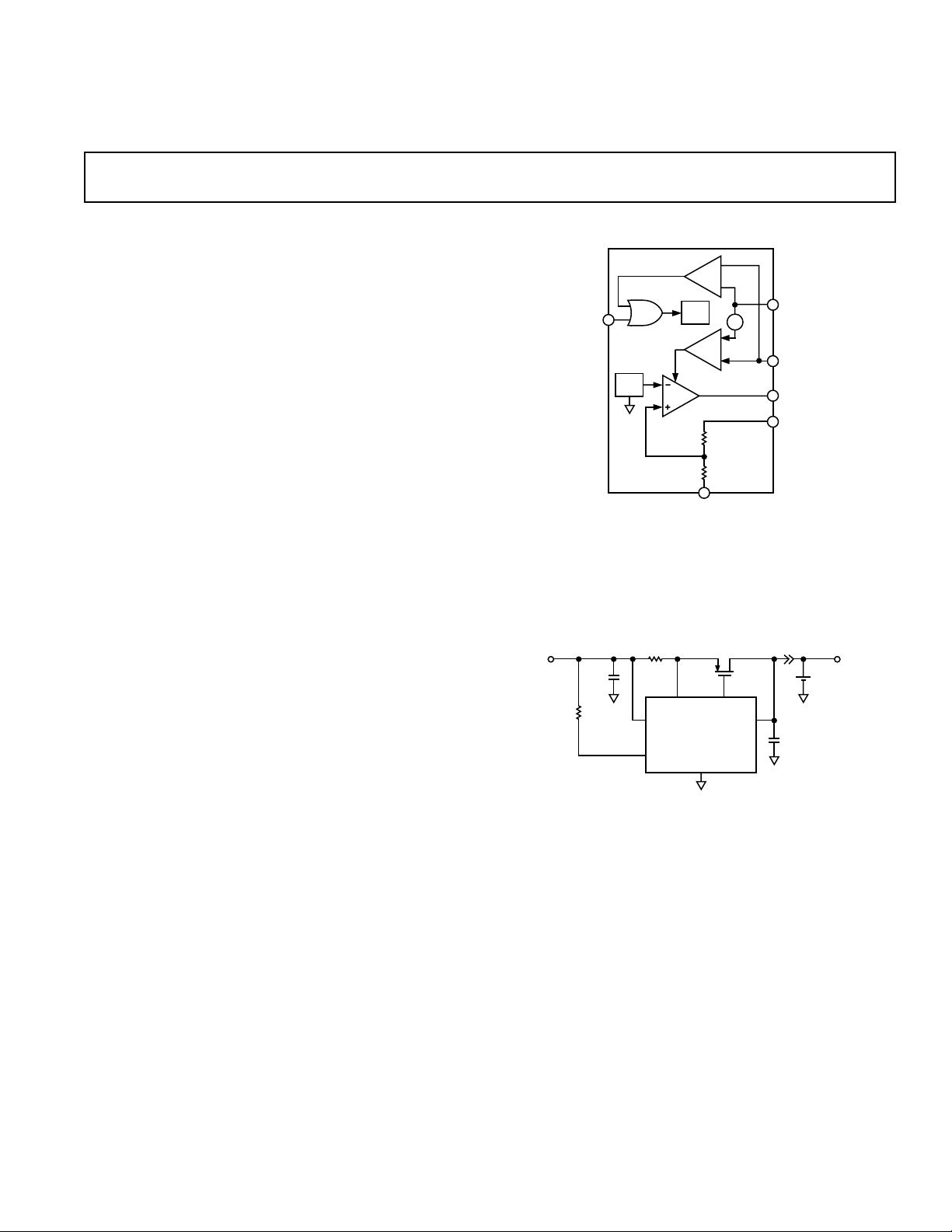
FUNCTIONAL BLOCK DIAGRAM
V
SD
V
REF
ADP3820
BIAS
+
–
50mV
GND
IN
IS
GATE
V
OUT
GENERAL DESCRIPTION
The ADP3820 is a precision single cell Li-Ion battery charge
controller that can be used with an external Power PMOS device to form a two-chip, low cost, low dropout linear battery
charger. It is available in two voltage options to accommodate
Li-Ion batteries with coke or graphite anodes. The ADP3820’s
high accuracy (±1%) low shutdown current (1 µA) and easy
charge current programming make this device especially attractive as a battery charge controller.
Charge current can be set by an external resistor. For example,
50 mΩ of resistance can be used to set the charge current to
1 A. Additional features of this device include foldback current
limit, overload recovery, and a gate-to-source voltage clamp to
protect the external MOSFET. The proprietary circuit also
minimizes the reverse leakage current from the battery if the
input voltage of the charger is disconnected. This feature eliminates the need for an external serial blocking diode.
The ADP3820 operates with a wide input voltage range from
4.5 V to 15 V. It is specified over the industrial temperature
range of –20°C to +85°C and is available in the ultrasmall
6-lead surface mount SOT-23-6 and 8-lead SOIC packages.
Figure 1. Li-Ion Charger Application Circuit
REV. A
Information furnished by Analog Devices is believed to be accurate and
reliable. However, no responsibility is assumed by Analog Devices for its
use, nor for any infringements of patents or other rights of third parties
which may result from its use. No license is granted by implication or
otherwise under any patent or patent rights of Analog Devices.
One Technology Way, P.O. Box 9106, Norwood, MA 02062-9106, U.S.A.
Tel: 781/329-4700 World Wide Web Site: http://www.analog.com
Fax: 781/326-8703 © Analog Devices, Inc., 1999

1
WARNING!
ESD SENSITIVE DEVICE
ADP3820–SPECIFICATIONS
(VIN = [V
Parameter Conditions Symbol Min Typ Max Units
INPUT VOLTAGE V
OUTPUT VOLTAGE ACCURACY V
IN
= V
VSD = 2 V
QUIESCENT CURRENT
Shutdown Mode V
= 0 V I
SD
Normal Mode VSD = 2 V I
GATE TO SOURCE CLAMP VOLTAGE 6 10 V
GATE DRIVE MINIMUM VOLTAGE
2
GATE DRIVE CURRENT (SINK/SOURCE) 1 mA
+ 1 V] TA = –20ⴗC to +85ⴗC, unless otherwise noted)
OUT
IN
+ 1 V to 15 V V
OUT
OUT
GND
GND
4.5 15 V
–1 +1 %
115µA
630 800 µA
0.7 V
GAIN
CURRENT LIMIT THRESHOLD VOLTAGE VIN – V
LOAD REGULATION I
∆
V
GS
∆
V
OUT
IS
= 10 mA to 1 A,
OUT
Circuit of Figure 1 –10 +10 mV
LINE REGULATION V
I
OUT
IN
= V
OUT
= 0.1 A
+ 1 V to 15 V
Circuit of Figure 1 (No Battery) –10 +10 mV
SD INPUT VOLTAGE V
IH
V
IL
SD INPUT CURRENT VSD = 0 V to 5 V I
OUTPUT REVERSE LEAKAGE CURRENT VIN = Floating I
NOTES
1
All limits at temperature extremes are guaranteed via correlation using standard Statistical Quality Control (SQC).
2
Provided gate-to-source clamp voltage is not exceeded.
Specifications subject to change without notice.
ABSOLUTE MAXIMUM RATINGS*
Input Voltage, V
Enable Input Voltage . . . . . . . . . . . . . . . 0.3 V to (V
Operating Ambient Temperature Range . . . . –20°C to +85°C
Storage Temperature Range . . . . . . . . . . . . –65°C to +150°C
, SO-8 Package . . . . . . . . . . . . . . . . . . . . . . . . 150°C/W
θ
JA
, SOT-23-6 Package . . . . . . . . . . . . . . . . . . . . 230°C/W
θ
JA
Lead Temperature (Soldering, 10 sec) . . . . . . . . . . . .+300°C
Vapor Phase (60 sec) . . . . . . . . . . . . . . . . . . . . . . . .+215°C
Infrared (15 sec) . . . . . . . . . . . . . . . . . . . . . . . . . . .+220°C
ESD Rating . . . . . . . . . . . . . . . . . . . . . . . . . . . . . . . . . . . 2 kV
*This is a stress rating only; operation beyond these limits can cause the device
to be permanently damaged.
␣ . . . . . . . . . . . . . . . . . . . . . . . . . . . . ⴙ20 V
IN
+ 0.3 V)
IN
Model Output Option* Code
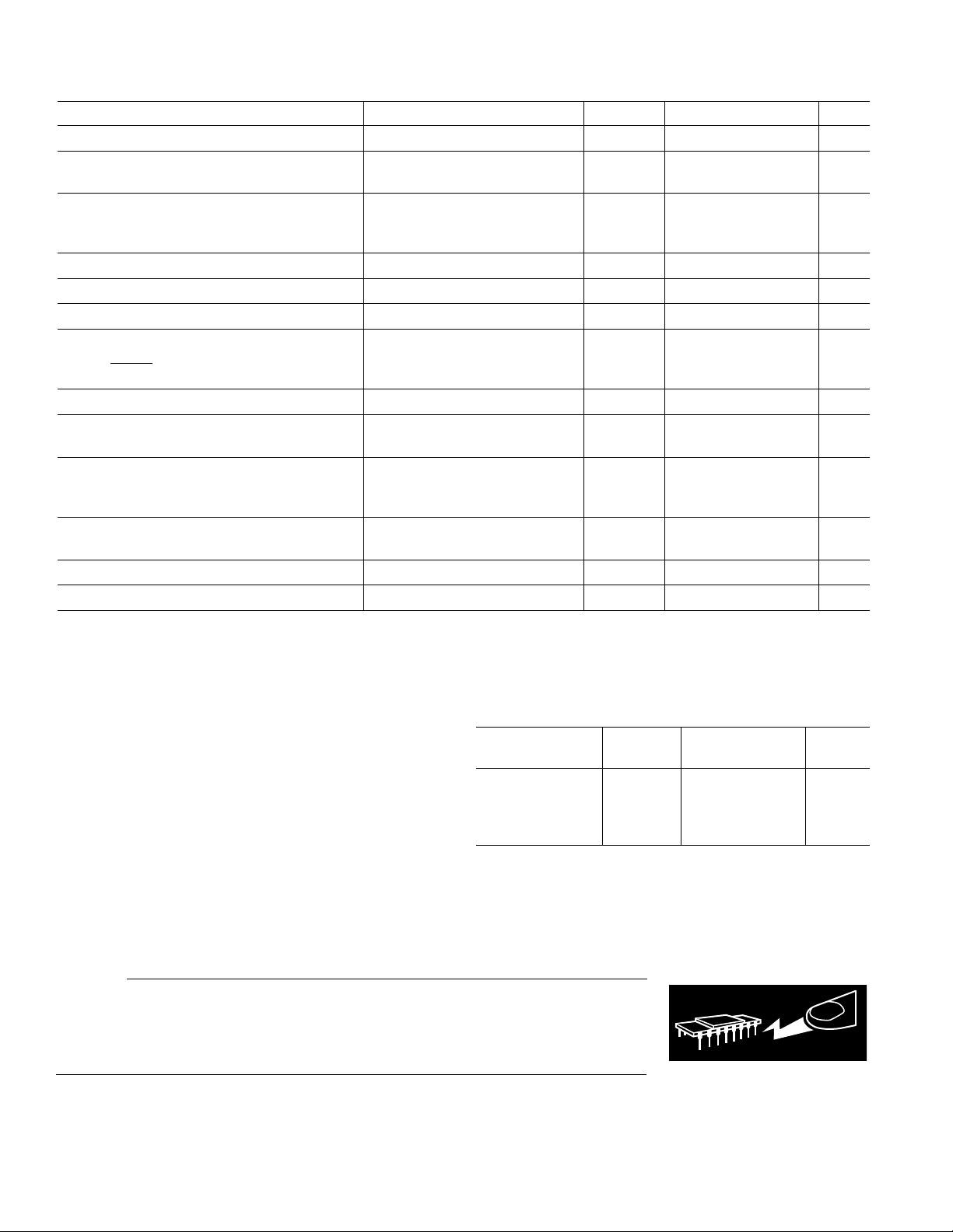
ADP3820ART-4.1 4.1 V RT-6 (SOT-23-6) BAC
ADP3820ART-4.2 4.2 V RT-6 (SOT-23-6) BBC
ADP3820AR-4.1 4.1 V SO-8
ADP3820AR-4.2 4.2 V SO-8
*SOT = Surface Mount Package. SO = Small Outline.
Contact the factory for availability of other output voltage options.
V
SD
SD
DISCH
ORDERING GUIDE
Voltage Package Marking
80 dB
40 75 mV
2.0 V
0.4 V
–15 +15 µA
35 µA
CAUTION
ESD (electrostatic discharge) sensitive device. Electrostatic charges as high as 4000 V readily
accumulate on the human body and test equipment and can discharge without detection.
Although the ADP3820 features proprietary ESD protection circuitry, permanent damage may
occur on devices subjected to high energy electrostatic discharges. Therefore, proper ESD
precautions are recommended to avoid performance degradation or loss of functionality.
–2– REV. A

ADP3820
PIN FUNCTION DESCRIPTIONS
Pin Pin
SOT-23-6 SO-8 Name Function
18SD Shutdown. Pulling this pin low
will disable the output.
2 7 GND Device Ground. This pin should
be tied to system ground closest
to the load.
35V
OUT
Output Voltage Sense. This pin
is connected to the MOSFET’s
drain and directly to the load for
optimal load regulation. Bypass
to ground with a 10 µF or larger
capacitor.
4 3 GATE Gate drive for the external
MOSFET.
54V
IN
Input Voltage. This is also the
positive terminal connection of
the current sense resistor.
6 1 IS Current Sense. Used to sense the
input current by monitoring the
voltage across the current sense
resistor. It is connected to the
more negative terminal of the
resistor as well as the power
MOSFET’s source pin. IS pin
should be tied to the V
pin if
IN
the current limit feature is not
used.
2, 6 NC No Connect.
1
IS
2
NC
3
GATE
V
4
IN
NC = NO CONNECT
PIN CONFIGURATIONS
SO-8 RT-6 (SOT-23-6)
ADP3820
TOP VIEW
(Not to Scale)
8
SD
7
GND
6
NC
5
V
OUT
GND
V
OUT
SD
1
ADP3820
2
TOP VIEW
3
(Not to Scale)
6
5
4
IS
V
IN
GATE
–3–REV. A
 Loading...