Analog Devices ADP3810 11 Datasheet

Secondary Side, Off-Line
a
FEATURES
Programmable Charge Current
High Precision Battery Voltage Limit
Precision 2.000 V Reference
Low Voltage Drop Current Sense: 300 mV Full Scale
Full Operation in Shorted and Open Battery Conditions
Drives Diode-Side of Optocoupler
Wide Operating Supply Range: 2.7 V to 16 V
Undervoltage Lockout
SO-8 Package
ADP3810
Internal Precision Voltage Divider for Battery Sense
Four Final Battery Voltage Options Available: 4.2 V,
8.4 V, 12.6 V, 16.8 V
ADP3811
Adjustable Final Battery Voltage
APPLICATIONS
Battery Charger Controller for:
LiIon Batteries (ADP3810)
NiCad, NiMH Batteries (ADP3811)
GENERAL DESCRIPTION
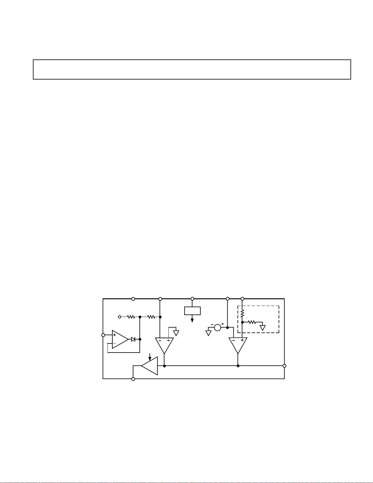
The ADP3810 and ADP3811 combine a programmable current
limit with a battery voltage limit to provide a constant current,
constant voltage battery charger controller. In secondary side,
Battery Charger Controllers
ADP3810/ADP3811
off-line applications, the output directly drives the diode side of
an optocoupler to give isolated feedback control of a primary
side PWM. The circuitry includes two gain (g
sion 2.0 V reference, a control input buffer, an Undervoltage
Lock Out (UVLO) comparator, an output buffer and an overvoltage comparator.
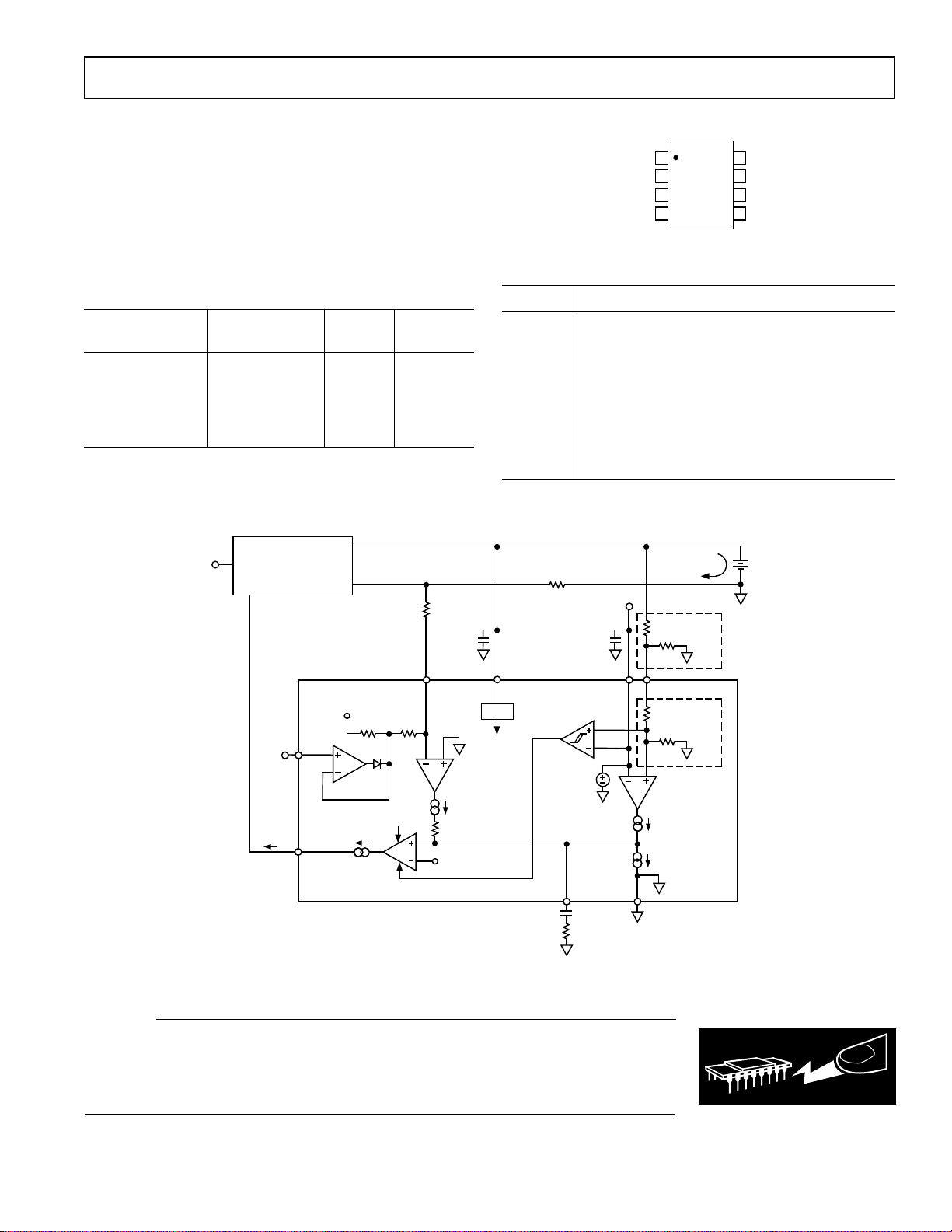
The current limit amplifier senses the voltage drop across an
external sense resistor to control the average current for charging a battery. The voltage drop can be adjusted from 25 mV
to 300 mV, giving a charging current limit from 100 mA to
1.2 amps with a 0.25 Ω sense resistor. An external dc voltage
on the V
input sets the voltage drop. Because this input
CTRL
is high impedance, a filtered PWM output can be used to set
the voltage.
As the battery voltage approaches its voltage limit, the voltage
sense amplifier takes over to maintain a constant battery voltage. The two amplifiers essentially operate in an “OR” fashion. Either the current is limited, or the voltage is limited.
The ADP3810 has internal thin-film resistors that are trimmed
to provide a precise final voltage for LiIon batteries. Four voltage options are available, corresponding to 1-4 LiIon cells as
follows: 4.2 V, 8.4 V, 12.6 V and 16.8 V.
The ADP3811 omits these resistors allowing any battery voltage to be programmed with external resistors.
) stages, a preci-
m
FUNCTIONAL BLOCK DIAGRAM
UVLO
GM
V
CS
GM1
V
CTRL
V
REF
GND
1.5MΩ 80kΩ
OUT
REV. 0
Information furnished by Analog Devices is believed to be accurate and
reliable. However, no responsibility is assumed by Analog Devices for its
use, nor for any infringements of patents or other rights of third parties
which may result from its use. No license is granted by implication or
otherwise under any patent or patent rights of Analog Devices.
V
V
CC
UVLO
UVLO
ADP3810/
ADP3811
One Technology Way, P.O. Box 9106, Norwood, MA 02062-9106, U.S.A.
Tel: 617/329-4700 World Wide Web Site: http://www.analog.com
Fax: 617/326-8703 © Analog Devices, Inc., 1996
V
SENSE
REF
ADP3810
R1
V
REF
ONLY
R2
GM2
COMP

ADP3810/ADP3811–SPECIFICATIONS
(–408C ≤ TA ≤ +858C, VCC = 10.0 V, unless otherwise noted)
ADP3810
Parameter Conditions Symbol Min Typ Max Units
CURRENT SENSE
Full-Scale Current Sense Voltage V
Minimum Current Sense Voltage 0.0 V ≤ V
Current Programming Input Range V
Gain (V
OUT/VCS
Control Input Bias Current V
VOLTAGE SENSE
Accuracy
2
—ADP3810 –1.0 +1.0 %
Input Resistance—ADP3810 4.2 V Option R
Input Resistance—ADP3810 8.4 V Option R
Input Resistance—ADP3810 12.6 V Option R
Input Resistance—ADP3810 16.8 V Option R
Offset Voltage—ADP3811 V
Bias Current—ADP3811 I
Gain (V
OUT/VSENSE
REFERENCE
Output Voltage C
1
= 1.2 V –315 –300 –285 mV
CTRL
)R
3
)
= 1 kΩ A
L
Pin I
CTRL
R
= 1 kΩ A
L
= 0.1 µF
L
≤ 0.1 V –32 –25 –18 mV
CTRL
4
CTRL
VCS
BCTRL
IN
IN
IN
IN
OS
B
VBAT
V
REF
0.0 1.2 V
74 86 dB
10 40 nA
210k Ω
420k Ω
630k Ω
840k Ω
–2.5 +2.5 mV
110 nA
60 74 dB
2.000 V
Accuracy
ADP3810 –1.0 +1.0 %
ADP3811 –1.8 +1.8 %
Load Regulation I
Line Regulation V
Output Voltage Noise 0.1 Hz to 10 Hz e
Load Current (Sourcing) I
= 0 mA to 5 mA –0.25 +0.25 %
LOAD
= 2.7 V to 16 V 0.004 0.02 %/V
CC
N
L
510 mA
35 µV p-p
OUTPUT
Output Current V
Saturation Voltage I
Gain (V
OUT/VCOMP
)R
= 2.7 V I
CC
= 4 mA, VCC–V
OUT
= 1 kΩ A
L
OUT
OUT
V
SAT
VOUT
46 mA
0.1 0.4 V
6 V/V
UNDERVOLTAGE LOCKOUT
Trip Point-On 2.65 2.7 V
Trip Point-Off 2.5 2.6 V
POWER SUPPLY
Operating Range 2.7 16 V
Quiescent Current V
Turn-Off Current V
≥ 2.7 V I
CC
≤ 2.5 V 0.5 1 mA
CC
Q
1.5 3 mA
OVERVOLTAGE COMPARATOR
Threshold
ADP3810 Percent Above Full Scale
ADP3811 Percent Above Full Scale
Response Time I
NOTES
1
20 kΩ resistor from current sense voltage to V
2
Applies to 4.2 V, 8.4 V, 12.6 V and 16.8 V options. Includes all error from offset voltage, bias current, resistor divider and voltage reference.
3
Does not include attenuation of input resistor divider for ADP3810.
4
0.1 µF load capacitor required for reference operation.
5
Full scale is the programmed final battery voltage: 4.2 V, 8.4 V, 12.6 V or 16.8 V for the ADP3810 or 2.0 V at V
All limits at temperature extremes are guaranteed via correlation using standard Statistical Quality Control (SQC) methods.
Specifications subject to change without notice.
CS
pin.
from 0 mA to 2 mA t
OUT
5
VOV%6%
5
VOV%6%
r
for the ADP3811.
SENSE
8 µs
–2–
REV. 0

ADP3810/ADP3811
ABSOLUTE MAXIMUM RATINGS
Supply Voltage, VCC . . . . . . . . . . . . . . . . . . . –0.4 V to 18 V
V
, VCS Input Range . . . . . . . . . . . . . . . . . . –0.4 V to V
CTRL
V
Input Range (ADP3811) . . . . . . . . . . . . –0.4 V to V
SENSE
V
Input Range (ADP3810) . . . . . . . . . . . –0.4 V to 20 V
SENSE
CC
CC
Maximum Power Dissipation . . . . . . . . . . . . . . . . . . 500 mW
Operating Temperature Range . . . . . . . . . . . –40°C to +85°C
Storage Temperature Range . . . . . . . . . . . . . –65°C to 150°C
Lead Temperature (Soldering, 10 sec) . . . . . . . . . . . .+300°C
ORDERING GUIDE
Temperature Package Battery
Model Range Option Voltage
ADP3810AR-4.2 –40°C to +85°C SO-8 4.2 V
ADP3810AR-8.4 –40°C to +85°C SO-8 8.4 V
ADP3810AR-12.6 –40°C to +85°C SO-8 12.6 V
ADP3810AR-16.8 –40°C to +85°C SO-8 16.8 V
ADP3811AR –40°C to +85°C SO-8 Adjustable
OUT
GND
RETURN
V
RCS
R3
0.1µF
IN
CTRL
DC/DC
CONVERTER
V
IN
PIN CONFIGURATION
8
V
SENSE
COMP
V
OUT
CS
1
ADP3810
2
ADP3811
TOP VIEW
3
(Not to Scale)
4
V
CC
7
V
REF
6
GND
V
5
CTRL
PIN DESCRIPTION
Mnemonic Function
V
SENSE
V
CS
V
REF
Battery Voltage Sense Input.
Current Sense Input.
Reference Output. Nominally 2.0 V.
COMP External Compensation Pin.
OUT Optocoupler Current Output Drive.
V
V
CTRL
CC
DC Control Input to Set Current Limit, 0 V to 1.2 V.
Positive Supply.
GND Ground Pin.
V
BAT
I
R1
R2
CHARGE
ADP3811
ONLY
R
CS
2.0V
0.1µF
BATTERY
V
V
REF
1.5MΩ
V
CTRL
BUFFER
I
OUT
OUT
CS
80kΩ
GM1
UVLO
GM3
200Ω
1.2V
V
CC
UVLO
UVLO
ADP3810/
ADP3811
COMP
REF
GND
V
R1
GM2
SENSE
ADP3810
R2
ONLY
V
V
REF
100µA
C
C
R
C
Figure 1. Simplified Battery Charger
CAUTION
ESD (electrostatic discharge) sensitive device. Electrostatic charges as high as 4000 V readily
accumulate on the human body and test equipment and can discharge without detection.
Although the ADP3810/ADP3811 features proprietary ESD protection circuitry, permanent
damage may occur on devices subjected to high energy electrostatic discharges. Therefore, proper
ESD precautions are recommended to avoid performance degradation or loss of functionality.
WARNING!
ESD SENSITIVE DEVICE
REV. 0
–3–

ADP3810/ADP3811
TEMPERATURE – °C
REFERENCE DROPOUT VOLTAGE – Volts
0.12
0.04
–50 –25 100
0255075
0.10
0.08
0.06
0.14
V
CC
= +10V
I
L
= 5mA
C
L
= 0.1µF
CONTROL VOLTAGE, V
CTRL
– Volts
CHARGE CURRENT – Amps
1.6
1.4
0
0 0.2 1.4
0.4 0.6 0.8 1.0
1.2
1.0
0.2
0.8
0.6
0.4
1.2
RCS = 0.25Ω
R3 = 20kΩ
–Typical Performance Characteristics
2.004
2 TYPICAL PARTS
2.002
2.000
1.998
1.996
REFERENCE VOLTAGE – Volts
1.994
–50 –25 100
0255075
TEMPERATURE – °C
V
CC
I
= 100µA
L
C
L
= +10V
= 0.1µF
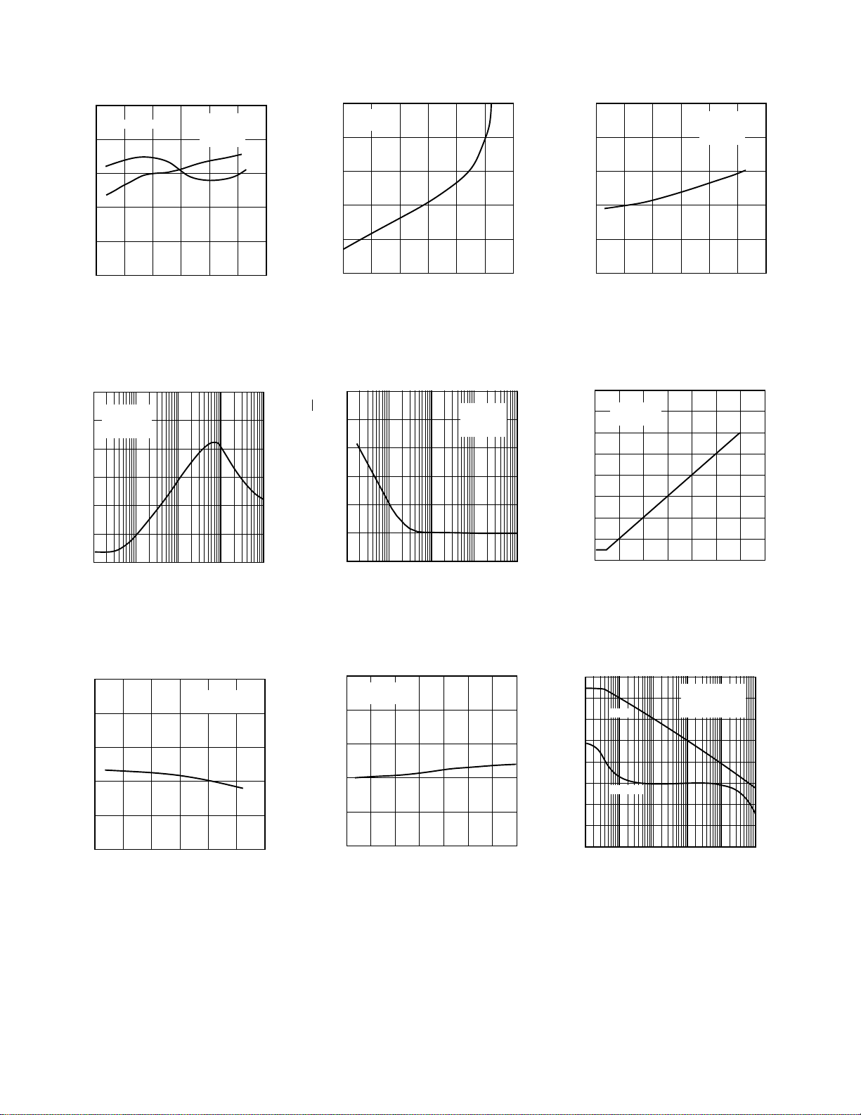
Figure 2. Reference Output Voltage
vs. Temperature for Two Typical Parts
–20
V
= +10V
CC
I
= 100µA
–30
L
C
= 0.1µF
L
–40
–50
PSRR – dB
–60
250
V
= +10V
CC
C
= 0.1µF
L
200
150
100
50
DROPOUT VOLTAGE – mV
0
03 18
6 9 12 15
LOAD CURRENT – mA
Figure 3. Reference Drop-Out Volt
age (V
3000
Hz
√
2500
2000
1500
1000
) vs. Load Current
CC–VREF
V
= +10V
CC
I
= 100µA
L
CL = 0.1µF
Figure 4. Reference Dropout Voltage
vs. Temperature
–70
–80
100 1k 1M
FREQUENCY – Hz
Figure 5. Reference PSRR vs.
Frequency
–294
–296
–298
–300
–302
CURRENT SENSE VOLTAGE – mV
–304
–50 –25 100
Figure 8. Full-Scale Current Sense
Voltage vs. Temperature
0255075
TEMPERATURE – °C
10k 100k
VCC = +10V
R3 = 20kΩ
500
REFERENCE NOISE DENSITY – nV/
0
1 10 10k
100 1k
FREQUENCY – Hz
Figure 6. Reference Noise Density
vs. Frequency
–294
V
= +10V
CC
R3 = 20kΩ
–296
–298
–300
–302
CURRENT SENSE VOLTAGE – mV
–304
24 16
6 8 10 12 14
SUPPLY VOLTAGE, VCC – Volts
Figure 9. Full-Scale Current Sense
Voltage vs. V
CC
–4–
Figure 7. Charge Current vs. Control
Voltage
100
80
GAIN
60
40
20
0
PHASE
–20
OPEN-LOOP GAIN – dB
–40
–60
100 1k
10 1M10k
FREQUENCY – Hz
C
T
V
COMP
A
CC
= 0.01µF
= +25°C
= +10V
100k
0
45
90
135
180
225
Figure 10. GM1 Open-Loop Gain and
Phase vs. Frequency
REV. 0
PHASE SHIFT – Degrees

ADP3810/ADP3811
SUPPLY VOLTAGE, VCC – Volts
1.0
0.5
–1.5
03 18
6 9 12 15
0
–0.5
–1.0
VOLTAGE SENSE ACCURACY – %
TA = +25°C
TEMPERATURE – °C
V
SENSE
BIAS CURRENT – nA
2.5
2.0
0
–50 –25 100
0255075
1.5
1.0
0.5
VCC = +10V
TEMPERATURE – °C
V
OV%
– %
12
10
2
–50 –25 100
0255075
8
6
4
VCC = +10V
100
80
GAIN
60
40
20
0
PHASE
–20
OPEN-LOOP GAIN – dB
–40
–60
100 1k
10 1M10k
FREQUENCY – Hz
C
T
A
V
CC
COMP
= +25°C
= +10V
= 0.01µF
100k
0
45
90
135
180
225
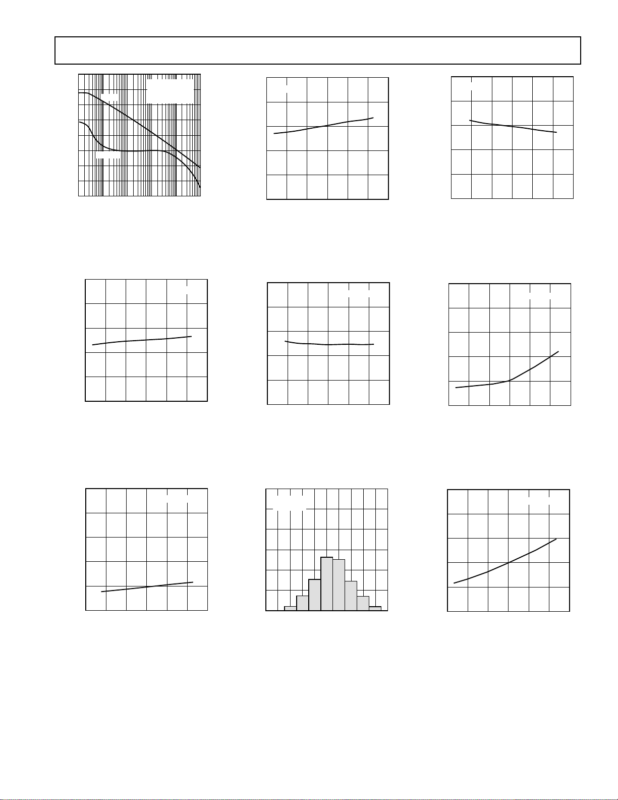
Figure 11. GM2 Open-Loop Gain and
Phase vs. Frequency
1.0
0.5
0
–0.5
GM2 OFFSET – mV
–1.0
VCC = +10V
1.0
V
= +10V
CC
0.5
0
–0.5
–1.0
VOLTAGE SENSE ACCURACY – %
PHASE SHIFT – Degrees
–1.5
–50 –25 1000 255075
TEMPERATURE – °C
Figure 12. ADP3810 Voltage Sense
Accuracy vs. Temperature
1.0
TA = +25°C
0.5
0
–0.5
GM2 OFFSET – mV
–1.0
Figure 13. ADP3810 Voltage Sense
Accuracy vs. V
CC
–1.5
–50 –25 100
0255075
TEMPERATURE – °C
Figure 14. ADP3811 GM2 Offset vs.
Temperature
2.5
2.0
1.5
1.0
BIAS CURRENT – nA
SENSE
0.5
V
0
03 18
6 9 12 15
SUPPLY VOLTAGE, VCC – Volts
Figure 17. ADP3811 V
Current vs. V
CC
TA = +25°C
Bias
SENSE
–1.5
03 18
6 9 12 15
SUPPLY VOLTAGE, VCC – Volts
Figure 15. ADP3811, GM2 Offset
vs. V
CC
120
V
= +10V
CC
T
= +25°C
A
100
80
60
40
QUANTITY – Parts
20
0
5.0 5.2 5.4 5.6 5.8 6.0 6.2 6.4 6.6 6.8 7.0
V
– %
OV%
Figure 18. Overvoltage Comparator
Distribution (V
OV%
)
Figure 16. ADP3811 V
SENSE
Bias
Current vs. Temperature
Figure 19. Overvoltage Comparator
Threshold (V
vs. Temperature
OV%)
REV. 0
–5–
 Loading...