Analog Devices ADP3806 b Datasheet

High Frequency Switch Mode
Li-Ion Battery Charger
ADP3806
FEATURES
Li-Ion Battery Charger
Three Battery Voltage Options
Selectable 12.525 V/16.700 V
Selectable 12.600 V/16.800 V
Adjustable
High End-of-Charge Voltage Accuracy
ⴞ0.4% @ 25ⴗC
ⴞ0.6% @ 5ⴗC to 55ⴗC
ⴞ0.7% @ 0ⴗC to 85ⴗC
Programmable Charge Current with Rail-to-Rail
Sensing
System Current Sense with Reverse Input Protection
Soft-Start Charge Current
Undervoltage Lockout
Bootstrapped Synchronous Drive for External NMOS
Programmable Oscillator Frequency
Oscillator SYNC Pin
Low Current Flag
Trickle Charge
APPLICATIONS
Portable Computers
Fast Chargers
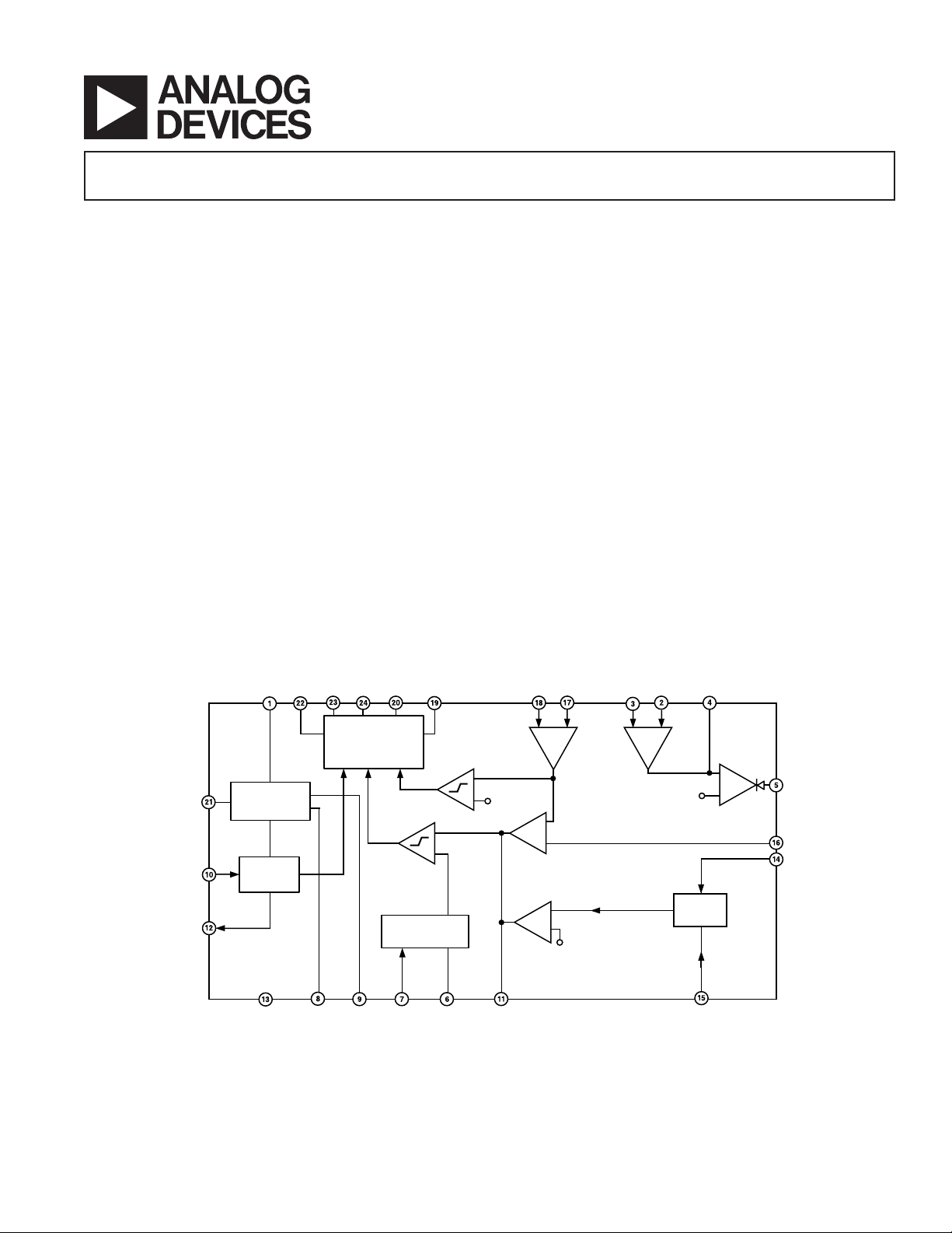
FUNCTIONAL BLOCK DIAGRAM
GENERAL DESCRIPTION
The ADP3806 is a complete Li-Ion battery-charging IC. The
device combines high output voltage accuracy with constant
current control to simplify the implementation of constantcurrent, constant-voltage (CCCV) chargers. The ADP3806 is
available in three options: The ADP3806-12.6 guarantees the
final battery voltage selected is 12.6 V or 16.8 V ± 0.6%, the
ADP3806-12.5 guarantees 12.525 V/16.7 V ± 0.6%, and the
ADP3806 is adjustable using two external resistors to set the
battery voltage. The current sense amplifier has rail-to-rail inputs
to accurately operate under low dropout and short-circuit conditions. The charge current is programmable with a dc voltage on
ISET. A second differential amplifier senses the system current
across an external sense resistor and outputs a linear voltage
on the ISYS pin. The bootstrapped synchronous driver allows
the use of two NMOS transistors for lower system cost.
BSTREG
SD
LC
VCC BST
VREF + VREG
UVLO
BIAS
LOGIC
CONTROL
DRVH DRVL
SW
BOOTSTRAPPED
SYNCHRONOUS
DRIVER
SD IN DRVLSD
VREF
PGND
DRVLSD
+
+
–
–
OSCILLATOR
ADP3806
AGND
REG
SYNC
CT
REV. B
Information furnished by Analog Devices is believed to be accurate and
reliable. However, no responsibility is assumed by Analog Devices for its
use, nor for any infringements of patents or other rights of third parties that
may result from its use. No license is granted by implication or otherwise
under any patent or patent rights of Analog Devices. Trademarks and
registered trademarks are the property of their respective owners.
CS+
CS–
+–
AMP1
–
+
+
V
–
TH
–
gm1
+
–
gm2
+
VREF
COMPREF
One Technology Way, P.O. Box 9106, Norwood, MA 02062-9106, U.S.A.
Tel: 781/329-4700 www.analog.com
Fax: 781/326-8703 © 2004 Analog Devices, Inc. All rights reserved.
SYS+ SYS– ISYS
+–
AMP2
2.5V
SELECT
12.6/16.8
BATSEL
–
+
LIMIT
ISET
BAT

ADP3806–SPECIFICATIONS
Parameter Conditions Symbol Min Typ Max Unit
BATTERY SENSE INPUT
ADP3806-12.6 V and 16.8 V
ADP3806-12.525 V and 16.7 V
= 25∞C, 13 V £ VCC £ 20 V V
T
A
5∞C £ T
0∞C £ T
Input Resistance Part in Operation R
Input Current Part in Shutdown I
BATTERY SENSE INPUT
ADP3806
= 2.5 V TA = 25∞C, 13 V £ VCC £ 20 V V
V
BAT
0∞C £ T
Input Current Operating BATSEL = Open, Part in Operation 0.2 1.0 mA
Input Current Shutdown BATSEL = 100 kW to GND, Part in Shutdown 0.2 1.0 mA
OSCILLATOR
Maximum Frequency
Frequency Variation
2
3
CT = 180 pF f
CT Charge Current I
0% Duty Cycle Threshold @ COMP Pin 1.0 V
Maximum Duty Cycle Threshold @ COMP Pin 2.5 V
SYNC Input High SYNC
SYNC Input Low SYNC
SYNC Input Current I
GATE DRIVE
On Resistance IL = 10 mA R
Rise, Fall Time C
Overlap Protection Delay DRVL Falling to DRVH Rising, t
DRVH Falling to DRVL Rising
SW Bias Current Part in Shutdown, V
BST Cap Refresh Threshold V
CURRENT SENSE AMPLIFIER
Input Common-Mode Range V
Input Differential Mode Range V
Input Offset Voltage
5
Gain
5
0 V £ V
Input Bias Current 0 V £ V
Input Offset Current 0 V £ V
Input Bias Current Part in Shutdown 0.2 1.0 mA
DRVL Shutdown Threshold Measured between V
SYSTEM CURRENT SENSE
6
Input Common-Mode Range SYS+ and SYS–, IL = 0 mA, V
Input Differential Range (V
Input Offset Voltage 0.5 mV
Input Bias Current, SYS+ V
Input Bias Current, SYS– V
Voltage Gain 10 V £ V
Output Range I
Limit Output Threshold V
Limit Output Voltage V
ISET INPUT
Charge Current Programming
Function 0.0 V < V
Programming Function Accuracy V
V
5∞C £ T
V
ISET Bias Current 0.0 V £ V
£ 55∞CV
A
£ 85∞CV
A
£ 85∞CV
A
= 1 nF, DRVL and DRVH tr, t
L
– V
BST
SW
and V
CS+
CS
SYS+
SYS(DM)
SYS(DM)
= 1 mA7, V
L
LIMIT
ISYS
ISET
ISET
CS(CM)
CS–
4
£ VCC V
CS(CM)
£ VCC, Part in Operation V
CS(CM)
£ VCC V
CS(CM)
) – (V
SYS–
= 0 V, V
= 0 V, V
SYS(CM)
SYS(CM)
£ 0.2 V, 50 kW Pull-up to 5 V V
> 2.65 V, I
£ 4.0 V V
ISET
= 4.0 V, 1 V £ V
= 0.50 V, 1 V £ V
£ 55∞C, V
A
= 5 V and 10 V
£ 4.0 V I
ISET
(@ 0ⴗC £ TA £ 100ⴗC, VCC = 16 V, unless otherwise noted.)
BAT
BAT
BAT
BAT
BAT(SD)
BAT
BAT
f
CT
CT
CT
H
L
SYNC
ON
f
OP
= 12.6 V 0.2 1.0 mA
SW
V
CS(CM)
V
CS(DM)
CS(VOS)
CS(IB)
CS(IOS)
and V
CS+
CS–
= 3 V V
ISYS
)V
= 16 V I
SYS(CM)
= 16 V I
SYS(CM)
V
)48 mV
CS(SD
SYS(CM)
SYS(DM)
B(SYS+)
B(SYS–)
£ VCC + 0.3 V, IL = 100 mA 48.5 50 51.5 V/V
> 6 V V
= 700 mAV
SINK
£ 16 V –5 ± 1.0 +5 %
CS(CM)
£ 10 V –30 ± 10 +30 %
CS(CM)
= 206 mV, –46.7 +33 %
ISET
ISYS
TH(LIMIT)
O(LIMIT)
ISET/VCS
B
–0.4 +0.4 %
–0.6 +0.6 %
–0.7 +0.7 %
250 350 kW
0.2 1.0 mA
–0.5 +0.5 %
–0.7 +0.7 %
1000 kHz
210 250 290 kHz
125 150 175 mA
2.2 V
0.8 V
0.2 1.0 mA
610 W
35 ns
50 ns
3.7 V
0.0 VCC + 0.3 V
0.0 160 mV
1.0 mV
25 V/V
50 100 mA
1.0 2.0 mA
4.0 VCC + 0.3 V
0 100 mV
200 300 mA
70 125 mA
0 5.0 V
2.3 2.5 2.7 V
0.1 0.2 V
25 V/V
0.2 1.0 mA
1
REV. B–2–

ADP3806
Parameter Conditions Symbol Min Typ Max Unit
BATSEL INPUT
V
= 12.6 V 2.0 V
BAT
= 16.8 V 0.8 V
V
BAT
BATSEL Input Current 0.2 5.0 mA
BOOST REGULATOR OUTPUT
Output Voltage CL = 0.1 mFV
Output Current
8
BSTREG
I
BSTREG
ANALOG REGULATOR OUTPUT
Output Voltage C
Output Current
8
= 10 nF V
L
I
REG
REG
PRECISION REFERENCE OUTPUT
Output Voltage V
Output Current
8
I
REF
REF
SHUTDOWN (SD)
ON SD
OFF SD
H
L
SD Input Current 0.2 1.0 mA
POWER SUPPLY
ON Supply Current No External Loads, UVLO £ VCC £ 20 V I
OFF Supply Current No External Loads, VCC £ 20 V I
UVLO Threshold Voltage Turn On V
SYON
SYOFF
UVLO
UVLO Hysteresis Turn Off 0.1 0.3 0.5 V
LC OUTPUT
Output Voltage Low High Current Mode9, I
Output Voltage High Low Current Mode
= 100 mA 0.1 0.4 V
SINK
10
OUTPUT REVERSE LEAKAGE
PROTECTION
Leakage Current VCC = Floating, V
= 12.6 V I
BAT
DISCH
OVERCURRENT COMPARATOR
Overcurrent Threshold V
Response Time VCS > 180 mV to COMP < 1 V t
CS(OC)
OC
OVERVOLTAGE COMPARATOR
Overvoltage Threshold V
Response Time V
NOTES
1
All limits at temperature extremes are guaranteed via correlation using standard Statistical Quality Control (SQC) methods.
2
Guaranteed by design, not tested in production.
3
If SYNC function is used, then f
4
VCS = (V
5
Accuracy guaranteed by ISET input, programming function accuracy specification.
6
System current sense is active during shutdown.
7
Load current is supplied through SYS+ pin.
8
Guaranteed output current from 0 to min specified value to maintain regulation.
9
V
BAT
10
V
) – (V
CS–
).
CS+
< 93% of final or VCS > 25 mV.
≥ 93% of final and VCS £ 25 mV.
BAT
Specifications subject to change without notice.
must be greater than fCT but less than 120% of fCT.
SYNC
> 120% to COMP < 1 V t
BAT
BAT(OV)
OV
6.8 7.0 7.2 V
3.0 5.0 mA
5.8 6.0 6.2 V
3.0 5.0 mA
2.47 2.5 2.53 V
0.5 1.1 mA
2.0 V
0.8 V
6.0 8.0 mA
1.0 5.0 mA
5.65 6.0 6.25 V
External V
15 mA
180 mV
2 ms
120 %
2 ms
REV. B
–3–

ADP3806
ABSOLUTE MAXIMUM RATINGS*
Input Voltage (VCC) . . . . . . . . . . . . . . . . . . . –0.3 V to +25 V
BAT, CS+, CS– . . . . . . . . . . . . . . . . . –0.3 V to VCC + 0.3 V
SYS+, SYS– . . . . . . . . . . . . . . . . . . . . . . . . . . –25 V to +25 V
BST . . . . . . . . . . . . . . . . . . . . . . . . . . . . . . . . . –0.3 V to +30 V
BST to SW . . . . . . . . . . . . . . . . . . . . . . . . . . . –0.3 V to +8 V
SW to PGND . . . . . . . . . . . . . . . . . . . . . . . . . . –4 V to +25 V
DRVL to PGND . . . . . . . . . . . . . . . . . . . . . . . –0.3 V to +8 V
ISET, BATSEL, SD, SYNC, CT,
LIMIT, ISYS, LC . . . . . . . . . . . . . . . . . . . –0.3 V to +10 V
COMP . . . . . . . . . . . . . . . . . . . . . . . . . . . . . . . –0.3 V to +3 V
GND to PGND . . . . . . . . . . . . . . . . . . . . . . . –0.3 V to +0.3 V
ORDERING GUIDE
Battery Package Package Quantity
Model Voltage Description Option per Reel
ADP3806JRU-REEL Adjustable TSSOP-24 RU-24 2500
ADP3806JRU-REEL7 Adjustable TSSOP-24 RU-24 1000
ADP3806JRU-12.5-RL 12.525 V/16.7 V TSSOP-24 RU-24 2500
ADP3806JRUZ-12.5RL
*
12.525 V/16.7 V TSSOP-24 RU-24 2500
ADP3806JRU-12.5-R7 12.525 V/16.7 V TSSOP-24 RU-24 1000
ADP3806JRU-12.6-RL 12.600 V/16.8 V TSSOP-24 RU-24 2500
ADP3806JRU-12.6-R7 12.600 V/16.8 V TSSOP-24 RU-24 1000
Operating Ambient Temperature Range . . . . . . 0∞C to 100∞C
. . . . . . . . . . . . . . . . . . . . . . . . . . . . . . . . . . . . . . . 115∞C/W
JA
Operating Junction Temperature Range . . . . . . 0∞C to 125∞C
Storage Temperature Range . . . . . . . . . . . . –65∞C to +150∞C
Lead Temperature Range (Soldering 10 sec) . . . . . . . . . 300∞C
*Stresses above those listed under Absolute Maximum Ratings may cause perma-
nent damage to the device. This is a stress rating only; functional operation of the
device at these or any other conditions above those listed in the operational
sections of this specification is not implied. Exposure to absolute maximum rating
conditions for extended periods may affect device reliability. Absolute maximum
ratings apply individually only, not in combination. Unless otherwise specified all
other voltages are referenced to GND.
*Z = Pb-free part.
CAUTION
ESD (electrostatic discharge) sensitive device. Electrostatic charges as high as 4000 V readily
accumulate on the human body and test equipment and can discharge without detection. Although the
ADP3806 features proprietary ESD protection circuitry, permanent damage may occur on devices
subjected to high energy electrostatic discharges. Therefore, proper ESD precautions are recommended
to avoid performance degradation or loss of functionality.
REV. B–4–

ADP3806
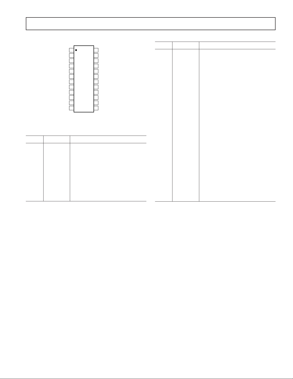
PIN CONFIGURATION
VCC
SYS–
SYS+
ISYS
LIMIT
SYNC
REG
REF
COMP
CT
SD
LC
1
2
3
4
5
ADP3806
6
TOP VIEW
(Not to Scale)
7
8
9
10
11
12
24
23
22
21
20
19
18
17
16
15
14
13
SW
DRVH
BST
BSTREG
DRVL
PGND
CS+
CS–
ISET
BATSEL
BAT
AGND
PIN FUNCTION DESCRIPTION
Pin No. Mnemonic Function
1 VCC Supply Voltage.
2 SYS– Negative System Current Sense Input.
3 SYS+ Positive System Current Sense Input.
4 ISYS System Current Sense Output.
5 LIMIT System Current Sense Limit Output.
6CTOscillator Timing Capacitor.
7 SYNC Oscillator Synchronization Pin.
8 REG 6.0 V Analog Regulator Output.
PIN FUNCTION DESCRIPTION(continued)
Pin No. Mnemonic Function
9 REF 2.5 V Precision Reference Output.
10 SD Shutdown Control Input.
11 COMP External Compensation Node.
12 LC Low Current Output.
13 AGND Analog Ground.
14 BAT Battery Sense Input.
2.5 V for ADP3806.
12.525 V/16.7 V for ADP3806-12.5.
12.6 V/16.8 V for ADP3806-12.6.
15 BATSEL Battery Voltage Sense Input.
High = 3 Cells, Low = 4 Cells.
16 ISET Charge Current Program Input.
17 CS– Negative Current Sense Input.
18 CS+ Positive Current Sense Input.
19 PGND Power Ground.
20 DRVL Low Drive Output Switches between
REG and PGND.
21 BSTREG 7.0 V Regulator Output for Boost.
22 BST Floating Bootstrap Supply for DRVH.
23 DRVH High Drive Output Switches between
SW and BST.
24 SW Buck Switching Node Reference for
DRVH.
REV. B
–5–
 Loading...