High Frequency Switch Mode
=
Li-Ion Battery Charger
Preliminary Technical Data ADP3804
FEATURES
Li-Ion Battery ChargerLi-Ion Battery Charger
Li-Ion Battery Charger
Li-Ion Battery ChargerLi-Ion Battery Charger
Fixed 12,525 V, 12.600 V, or Adjustable BatteryFixed 12,525 V, 12.600 V, or Adjustable Battery
Fixed 12,525 V, 12.600 V, or Adjustable Battery
Fixed 12,525 V, 12.600 V, or Adjustable BatteryFixed 12,525 V, 12.600 V, or Adjustable Battery
VoltageVoltage
Voltage
VoltageVoltage
High End-of-Charge Voltage AccuracyHigh End-of-Charge Voltage Accuracy
High End-of-Charge Voltage Accuracy
High End-of-Charge Voltage AccuracyHigh End-of-Charge Voltage Accuracy
ⴞⴞ
0.4% @ +250.4% @ +25
ⴞ
0.4% @ +25
ⴞⴞ
0.4% @ +250.4% @ +25
ⴞⴞ
0.6% @ 50.6% @ 5
ⴞ
0.6% @ 5
ⴞⴞ
0.6% @ 50.6% @ 5
ⴞⴞ
0.75% @ 00.75% @ 0
ⴞ
0.75% @ 0
ⴞⴞ
0.75% @ 00.75% @ 0
Programmable Charge Current withProgrammable Charge Current with
Programmable Charge Current with
Programmable Charge Current withProgrammable Charge Current with
Rail-to-Rail SensingRail-to-Rail Sensing
Rail-to-Rail Sensing
Rail-to-Rail SensingRail-to-Rail Sensing
System Current Sense with Reverse Input ProtectionSystem Current Sense with Reverse Input Protection
System Current Sense with Reverse Input Protection
System Current Sense with Reverse Input ProtectionSystem Current Sense with Reverse Input Protection
Softstart Charge CurrentSoftstart Charge Current
Softstart Charge Current
Softstart Charge CurrentSoftstart Charge Current
Undervoltage LockoutUndervoltage Lockout
Undervoltage Lockout
Undervoltage LockoutUndervoltage Lockout
Boosted Synchronous Drive For External NMOSBoosted Synchronous Drive For External NMOS
Boosted Synchronous Drive For External NMOS
Boosted Synchronous Drive For External NMOSBoosted Synchronous Drive For External NMOS
Programmable Oscillator FrequencyProgrammable Oscillator Frequency
Programmable Oscillator Frequency
Programmable Oscillator FrequencyProgrammable Oscillator Frequency
Oscillator SYNC PinOscillator SYNC Pin
Oscillator SYNC Pin
Oscillator SYNC PinOscillator SYNC Pin
Constant Current/Constant Voltage FlagConstant Current/Constant Voltage Flag
Constant Current/Constant Voltage Flag
Constant Current/Constant Voltage FlagConstant Current/Constant Voltage Flag
Trickle ChargeTrickle Charge
Trickle Charge
Trickle ChargeTrickle Charge
APPLICATIONS
Portable ComputersPortable Computers
Portable Computers
Portable ComputersPortable Computers
Fast ChargersFast Chargers
Fast Chargers
Fast ChargersFast Chargers
ⴗⴗ
CC
ⴗ
C
ⴗⴗ
CC
ⴗⴗ
C to 55C to 55
ⴗ
C to 55
ⴗⴗ
C to 55C to 55
ⴗⴗ
C to 85C to 85
ⴗ
C to 85
ⴗⴗ
C to 85C to 85
ⴗⴗ
CC
ⴗ
C
ⴗⴗ
CC
ⴗⴗ
CC
ⴗ
C
ⴗⴗ
CC
PRELIMINAR Y
TECHNICAL
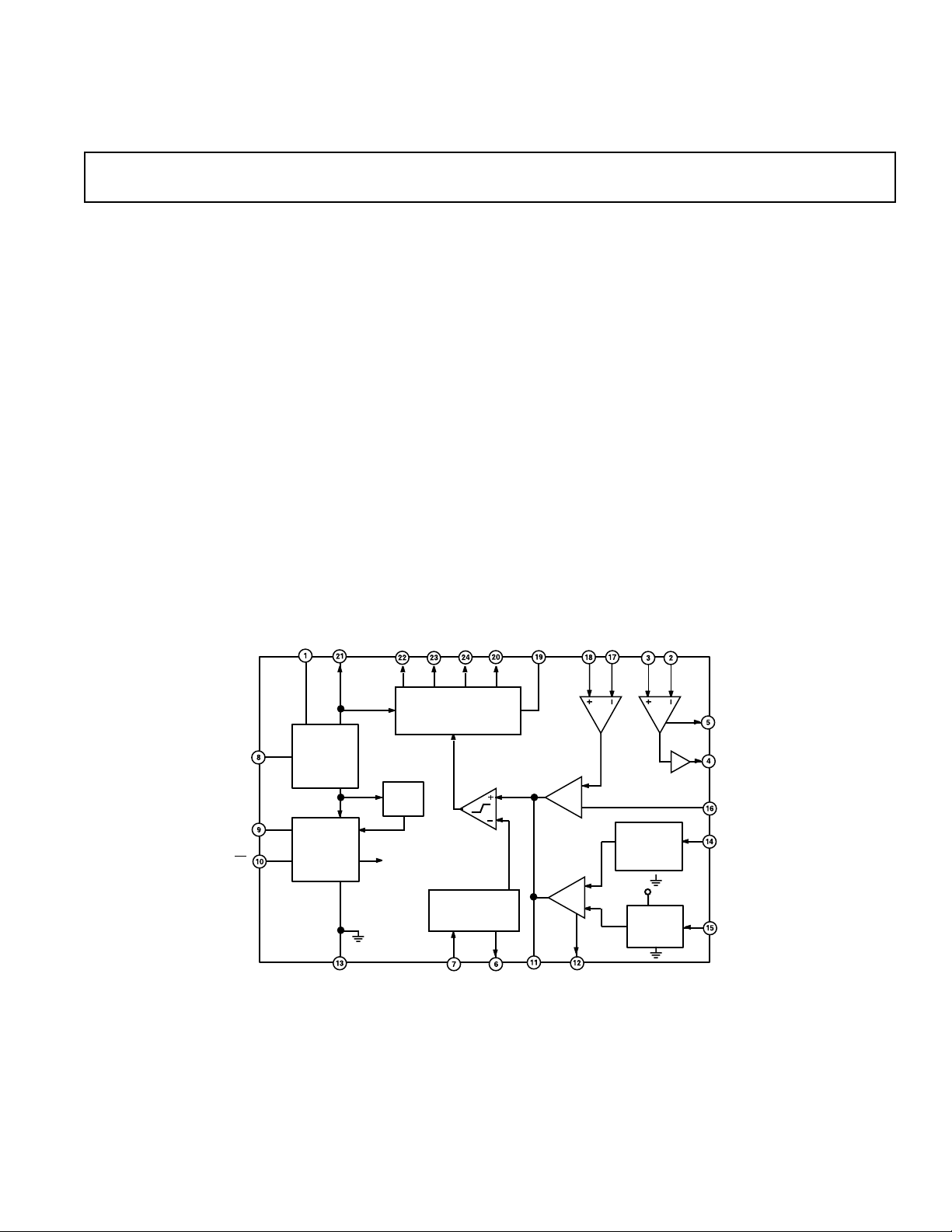
FUNCTIONAL BLOCK DIAGRAMFUNCTIONAL BLOCK DIAGRAM
FUNCTIONAL BLOCK DIAGRAM
FUNCTIONAL BLOCK DIAGRAMFUNCTIONAL BLOCK DIAGRAM
GENERAL DESCRIPTION
The ADP3804 is a complete Li-Ion battery charging IC. The
device combines high output voltage accuracy with constant
current control to simplify the implementation of ConstantCurrent, Constant-Voltage (CCCV) chargers. The ADP3804 is
available in two options. The ADP3804-12.6 guarantees the
final battery voltage to 12.6 V ± 0.6%, the ADP3804-12.5
guarantees 12.525 V ± 0.6% and the ADP3804 is adjustable
using two external resistors to set the battery voltage. The
current sense amplifier has rail-to-rail inputs to accurately
operate under low drop out and short circuit conditions. The
charge current is programmable with a DC voltage on ISET. A
second differential amplifier senses the system current across an
external sense resistor and outputs a linear voltage on the ISYS
pin. The boosted synchronous driver allows the use of two
NMOS transistors for lower system cost.
DA T A
REG
REF
SD
VCC
REGULATOR
REGULATOR
REFERENCE
ADP3804
BSTREG BST DRVH SW DRVL PGND
BOOSTED
SYNCHRONOUS
BOOST
+
SUPPLY
+
BIAS
AGND
UVLO
VREF
DRIVER
OSCILLATOR
SYNC
CT
COMP
CS+ SYSCS SYS+
AMP
1
g
m1
g
m2
CCCV
AMP
2
INPUT
DIVIDER
ADP3804-12.6
ADP3804-12.5
VREF
BATTERY
ADJUST
LIMIT
ISYS
ISET
BAT
ADJ
REV. PrI 12/5/00
Information furnished by Analog Devices is believed to be accurate and
reliable. However, no responsibility is assumed by Analog Devices for its
use, nor for any infringements of patents or other rights of third parties
which may result from its use. No license is granted by implication or
otherwise under any patent or patent rights of Analog Devices.
One Technology Way, P.O. Box 9106, Norwood, MA 02062-9106, U.S.A.
Tel: 781/329-4700 World Wide Web Site: http://www.analog.com
Fax: 781/326-8703 © Analog Devices, Inc., 2000

1
ADP3804–SPECIFICATIONS
(@ 0ⴗC £ TA £ 100ⴗC, VCC =16 V, unless otherwise noted)
Parameter Conditions Symbol Min Typ Max Units
BATTERY SENSE INPUT
ADP3804-12.6
V
BAT
V
BAT
V
BAT
V
BAT
Input Resistance Part in Operation R
Input Current Part in Shutdown I
TA = +25°C V
5°C
£ T
£ 55°C
0°C
0°C
A
£ T
£ 85°CV
A
£ T
£ 100°C
A
BAT
V
BAT
BAT
V
BAT
BAT
BAT(SD)
12.550 12.6 12.650 V
12.524 12.676 V
12.505 12.695 V
12.474 12.726 V
400 500 kW
0.2 1.0 mA
BATTERY SENSE INPUT
ADP3804-12.5
V
BAT
V
BAT
V
BAT
V
BAT
Input Resistance Part in Operation R
Input Current Part in Shutdown I
TA = +25°C V
5°C
£ T
£ 55°C
0°C
0°C
A
£ T
£ 85°CV
A
£ T
£ 100°C
A
BAT
V
BAT
BAT
V
BAT
BAT
BAT(SD)
12.475 12.525 12.575 V
12.450 12.600 V
12.430 12.620 V
12.400 12.650 V
400 500 kW
0.2 1.0 mA
BATTERY SENSE INPUT
ADP3804
V
BAT
V
BAT
V
BAT
TA = +25°C V
0°C
£ T
£ 85°CV
£ T
A
£ 100°C
A
0°C
BAT
BAT
V
BAT
2.490 2.500 2.510 V
2.481 2.519 V
2.475 2.525 V
Input Current 0.2 1.0 mA
OSCILLATOR
Maximum Frequency
Frequency Variation
CT Charge Current I
2
3
CT = 150 pF f
PRELIMINAR Y
f
CT
CT
CT
1000 kHz
215 250 285 kHz
130 150 170 mA
0% Duty Cycle Threshold @ COMP Pin 1.0 V
Maximum Duty Cycle Threshold @ COMP Pin 2.5 V
SYNC Input High SYNC
SYNC Input Low SYNC
SYNC Input Current I
TECHNICAL
DA T A
SYNC
2.0 V
H
L
0.2 1.0 mA
0.8 V
GATE DRIVE
On Resistance IL = 10 mA R
Rise, Fall Time C
= 1 nF, DRVL and DRVH tr , t
L
Overlap Protection Delay DRVL Falling to DRVH Rising, t
ON
f
OP
610W
35 ns
50 ns
DRVH Falling to DRVL Rising
SW Bias Current Part in Shutdown, VSW = 12.6 V 0.2 1.0 µA
CURRENT SENSE AMPLIFIER
Input Common-mode Range V
Input Differential Mode Range V
Input Offset Voltage
5
Gain
5
and V
CS+
4
CS
0 V £ V
Input Bias Current 0 V £ V
Input Offset Current 0 V £ V
CS–
£ VCC V
CS(CM)
£ VCC, Part in Operation V
CS(CM)
£ VCC V
CS(CM)
V
CS(CM)
V
CS(DM)
CS(VOS)
CS(IB)
CS(IOS)
0.0
VCC+0.3
V
0.0 160 mV
1.0 mV
25 V/V
50 100 µA
1.0 2.0 µA
Input Bias Current Part in Shutdown 0.2 1.0 µA
SYSTEM CURRENT SENSE
Input Common Mode Range
Input Differential Range (V
6
SYS+ and SYS- V
SYS+
) - (V
)V
SYS-
SYS(CM)
SYS(DM)
4.0 VCC+0.3 V
0 100 mV
Input Offset Voltage 1.0 2.0 mV
Input Bias Current, SYS+ V
Input Bias Current, SYS- V
Voltage Gain 10 V £ V
Output Range
IL = 1 mA7,
SYS(DM)
SYS(DM)
= 0 V, V
= 0 V, V
£ VCC + 0.3V 48 50 52 V/V
SYS(CM)
V
SYS(CM)
Limit Output Threshold V
Limit Output Voltage V
ISYS
> V
TH(LIMIT)
= 16 V I
SYS(CM)
= 16 V I
SYS(CM)
> 6 V V
, I
= 1 mA V
SINK
B(SYS+)
B(SYS–)
ISYS
TH(LIMIT)
O(LIMIT)
50 100 mA
25 50 mA
0 5.0 V
2.4 2.5 2.6 V
0.1 0.2 V
–2–
REV. PrI

ADP3804
Parameter Conditions Symbol Min Typ Max Units
ISET INPUT
Charge Current Programming
<
V
Function 0.0 V
Programming Function Accuracy V
V
ISET
ISET
= 4.0 V
= 0.50 V,
ISET Bias Current 0.0 V £ V
ISET
ISET
£ 4.0 V
£ 4.0 V
ADJ INPUT
V
Adjustment V
BAT
Adjustment V
V
BAT
Disable Threshold 4.4 4.6 V
V
BAT
ADJ Bias Current 1.0 V £ V
= 1 V –4.8 –5.0 –5.2 %
ADJ
= 4 V +4.8 +5.0 +5.2 %
ADJ
£ 4.0 V 0.2 1.0
ADJ
BOOST REGULATOR
OUTPUT
Output Voltage C
= 0.1 mFV
L
Output Current I
ANALOG REGULATOR
OUTPUT
Output Voltage CL = 10 nF V
Output Current
PRECISION REFERENCE
OUTPUT
Output Voltage V
Output Current I
SHUTDOWN (SD)
ON SD
OFF SD
SD Input Current 0.2 1.0
PRELIMINAR Y
POWER SUPPLY
ON Supply Current No External Loads I
OFF Supply Current No External Loads I
Threshold Voltage Turn On V
UVLO
TECHNICAL
DA T A
UVLO Hysteresis Turn Off 0.1 0.3 0.5 V
CCCV OUTPUT
Output Voltage Low Constant Current Mode8, V
= 100 µA 0.1 0.4 V
I
SINK
Output Voltage High Constant Voltage Mode9, V
= 2.5 V,
ISET
= 2.5 V external V
ISET
OUTPUT REVERSE
LEAKAGE PROTECTION
Leakage Current VCC = Floating, V
1
All limits at temperature extremes are guaranteed via correlation using standard Statistical Quality Control (SQC) methods.
2
Guaranteed by design, not tested in production.
3
If SYNC function is used, then f
4
VCS = (V
5
Accuracy guaranteed by ISET INPUT, Programming Function Accuracy specification.
6
System current sense is active during shutdown.
7
Load current is supplied through SYS+ pin.
8
V
BAT
9
V
BAT
Specifications subject to change without notice.
) – (V
CS–
).
CS+
< 95% of final or VCS > 80% of ISET programmed value.
³³
³ 95% of final and VCS
³³
must be greater than fCT, but less than 120% of fCT.
SYNC
££
£ 80% of ISET programmed value.
££
= 12.6 V I
BAT
V
ISET/VCS
I
B
BSTREG
BSTREG
REG
I
REG
REF
REF
H
L
SYON
SYOFF
UVLO
DISCH
25
–5 ±1.0 +5
–20 ±10 +20
0.2 1.0
V/V
%
%
mA
mA
6.8 7.0 7.2 V
35 mA
5..8 6.0 6.2 V
3.0 5.0 mA
2.475 2.5 2.525 V
0.5 1.1 mA
2.0 V
0.8 V
m
A
8.0 10 mA
2.0 10
m
A
5.75 6.0 6.25 V
3.0 10 µA
REV. PrI
–3–
 Loading...