

High Frequency Switch Mode
=
Li-Ion Battery Charger
Preliminary Technical Data ADP3804
FEATURES
Li-Ion Battery ChargerLi-Ion Battery Charger
Li-Ion Battery Charger
Li-Ion Battery ChargerLi-Ion Battery Charger
Fixed 12,525 V, 12.600 V, or Adjustable BatteryFixed 12,525 V, 12.600 V, or Adjustable Battery
Fixed 12,525 V, 12.600 V, or Adjustable Battery
Fixed 12,525 V, 12.600 V, or Adjustable BatteryFixed 12,525 V, 12.600 V, or Adjustable Battery
VoltageVoltage
Voltage
VoltageVoltage
High End-of-Charge Voltage AccuracyHigh End-of-Charge Voltage Accuracy
High End-of-Charge Voltage Accuracy
High End-of-Charge Voltage AccuracyHigh End-of-Charge Voltage Accuracy
ⴞⴞ
0.4% @ +250.4% @ +25
ⴞ
0.4% @ +25
ⴞⴞ
0.4% @ +250.4% @ +25
ⴞⴞ
0.6% @ 50.6% @ 5
ⴞ
0.6% @ 5
ⴞⴞ
0.6% @ 50.6% @ 5
ⴞⴞ
0.75% @ 00.75% @ 0
ⴞ
0.75% @ 0
ⴞⴞ
0.75% @ 00.75% @ 0
Programmable Charge Current withProgrammable Charge Current with
Programmable Charge Current with
Programmable Charge Current withProgrammable Charge Current with
Rail-to-Rail SensingRail-to-Rail Sensing
Rail-to-Rail Sensing
Rail-to-Rail SensingRail-to-Rail Sensing
System Current Sense with Reverse Input ProtectionSystem Current Sense with Reverse Input Protection
System Current Sense with Reverse Input Protection
System Current Sense with Reverse Input ProtectionSystem Current Sense with Reverse Input Protection
Softstart Charge CurrentSoftstart Charge Current
Softstart Charge Current
Softstart Charge CurrentSoftstart Charge Current
Undervoltage LockoutUndervoltage Lockout
Undervoltage Lockout
Undervoltage LockoutUndervoltage Lockout
Boosted Synchronous Drive For External NMOSBoosted Synchronous Drive For External NMOS
Boosted Synchronous Drive For External NMOS
Boosted Synchronous Drive For External NMOSBoosted Synchronous Drive For External NMOS
Programmable Oscillator FrequencyProgrammable Oscillator Frequency
Programmable Oscillator Frequency
Programmable Oscillator FrequencyProgrammable Oscillator Frequency
Oscillator SYNC PinOscillator SYNC Pin
Oscillator SYNC Pin
Oscillator SYNC PinOscillator SYNC Pin
Constant Current/Constant Voltage FlagConstant Current/Constant Voltage Flag
Constant Current/Constant Voltage Flag
Constant Current/Constant Voltage FlagConstant Current/Constant Voltage Flag
Trickle ChargeTrickle Charge
Trickle Charge
Trickle ChargeTrickle Charge
APPLICATIONS
Portable ComputersPortable Computers
Portable Computers
Portable ComputersPortable Computers
Fast ChargersFast Chargers
Fast Chargers
Fast ChargersFast Chargers
ⴗⴗ
CC
ⴗ
C
ⴗⴗ
CC
ⴗⴗ
C to 55C to 55
ⴗ
C to 55
ⴗⴗ
C to 55C to 55
ⴗⴗ
C to 85C to 85
ⴗ
C to 85
ⴗⴗ
C to 85C to 85
ⴗⴗ
CC
ⴗ
C
ⴗⴗ
CC
ⴗⴗ
CC
ⴗ
C
ⴗⴗ
CC
PRELIMINAR Y
TECHNICAL
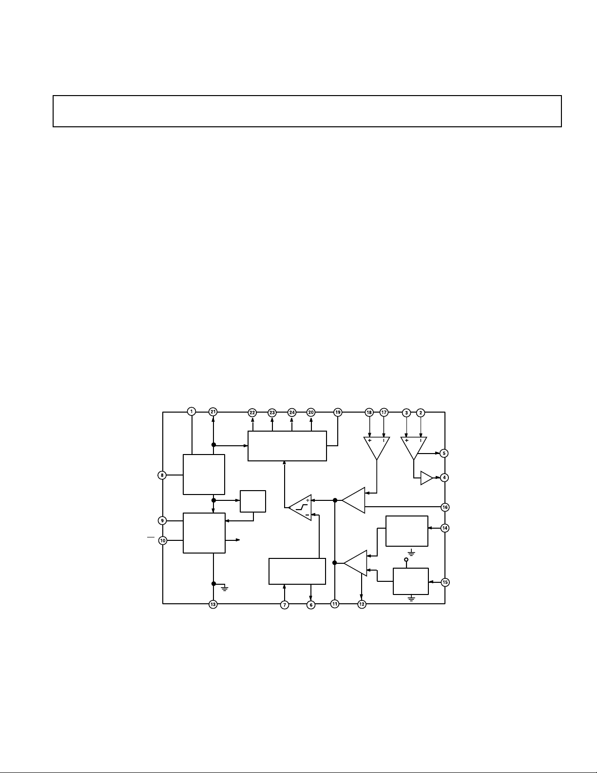
FUNCTIONAL BLOCK DIAGRAMFUNCTIONAL BLOCK DIAGRAM
FUNCTIONAL BLOCK DIAGRAM
FUNCTIONAL BLOCK DIAGRAMFUNCTIONAL BLOCK DIAGRAM
GENERAL DESCRIPTION
The ADP3804 is a complete Li-Ion battery charging IC. The
device combines high output voltage accuracy with constant
current control to simplify the implementation of ConstantCurrent, Constant-Voltage (CCCV) chargers. The ADP3804 is
available in two options. The ADP3804-12.6 guarantees the
final battery voltage to 12.6 V ± 0.6%, the ADP3804-12.5
guarantees 12.525 V ± 0.6% and the ADP3804 is adjustable
using two external resistors to set the battery voltage. The
current sense amplifier has rail-to-rail inputs to accurately
operate under low drop out and short circuit conditions. The
charge current is programmable with a DC voltage on ISET. A
second differential amplifier senses the system current across an
external sense resistor and outputs a linear voltage on the ISYS
pin. The boosted synchronous driver allows the use of two
NMOS transistors for lower system cost.
DA T A
REG
REF
SD
VCC
REGULATOR
REGULATOR
REFERENCE
ADP3804
BSTREG BST DRVH SW DRVL PGND
BOOSTED
SYNCHRONOUS
BOOST
+
SUPPLY
+
BIAS
AGND
UVLO
VREF
DRIVER
OSCILLATOR
SYNC
CT
COMP
CS+ SYSCS SYS+
AMP
1
g
m1
g
m2
CCCV
AMP
2
INPUT
DIVIDER
ADP3804-12.6
ADP3804-12.5
VREF
BATTERY
ADJUST
LIMIT
ISYS
ISET
BAT
ADJ
REV. PrI 12/5/00
Information furnished by Analog Devices is believed to be accurate and
reliable. However, no responsibility is assumed by Analog Devices for its
use, nor for any infringements of patents or other rights of third parties
which may result from its use. No license is granted by implication or
otherwise under any patent or patent rights of Analog Devices.
One Technology Way, P.O. Box 9106, Norwood, MA 02062-9106, U.S.A.
Tel: 781/329-4700 World Wide Web Site: http://www.analog.com
Fax: 781/326-8703 © Analog Devices, Inc., 2000

1
ADP3804–SPECIFICATIONS
(@ 0ⴗC £ TA £ 100ⴗC, VCC =16 V, unless otherwise noted)
Parameter Conditions Symbol Min Typ Max Units
BATTERY SENSE INPUT
ADP3804-12.6
V
BAT
V
BAT
V
BAT
V
BAT
Input Resistance Part in Operation R
Input Current Part in Shutdown I
TA = +25°C V
5°C
£ T
£ 55°C
0°C
0°C
A
£ T
£ 85°CV
A
£ T
£ 100°C
A
BAT
V
BAT
BAT
V
BAT
BAT
BAT(SD)
12.550 12.6 12.650 V
12.524 12.676 V
12.505 12.695 V
12.474 12.726 V
400 500 kW
0.2 1.0 mA
BATTERY SENSE INPUT
ADP3804-12.5
V
BAT
V
BAT
V
BAT
V
BAT
Input Resistance Part in Operation R
Input Current Part in Shutdown I
TA = +25°C V
5°C
£ T
£ 55°C
0°C
0°C
A
£ T
£ 85°CV
A
£ T
£ 100°C
A
BAT
V
BAT
BAT
V
BAT
BAT
BAT(SD)
12.475 12.525 12.575 V
12.450 12.600 V
12.430 12.620 V
12.400 12.650 V
400 500 kW
0.2 1.0 mA
BATTERY SENSE INPUT
ADP3804
V
BAT
V
BAT
V
BAT
TA = +25°C V
0°C
£ T
£ 85°CV
£ T
A
£ 100°C
A
0°C
BAT
BAT
V
BAT
2.490 2.500 2.510 V
2.481 2.519 V
2.475 2.525 V
Input Current 0.2 1.0 mA
OSCILLATOR
Maximum Frequency
Frequency Variation
CT Charge Current I
2
3
CT = 150 pF f
PRELIMINAR Y
f
CT
CT
CT
1000 kHz
215 250 285 kHz
130 150 170 mA
0% Duty Cycle Threshold @ COMP Pin 1.0 V
Maximum Duty Cycle Threshold @ COMP Pin 2.5 V
SYNC Input High SYNC
SYNC Input Low SYNC
SYNC Input Current I
TECHNICAL
DA T A
SYNC
2.0 V
H
L
0.2 1.0 mA
0.8 V
GATE DRIVE
On Resistance IL = 10 mA R
Rise, Fall Time C
= 1 nF, DRVL and DRVH tr , t
L
Overlap Protection Delay DRVL Falling to DRVH Rising, t
ON
f
OP
610W
35 ns
50 ns
DRVH Falling to DRVL Rising
SW Bias Current Part in Shutdown, VSW = 12.6 V 0.2 1.0 µA
CURRENT SENSE AMPLIFIER
Input Common-mode Range V
Input Differential Mode Range V
Input Offset Voltage
5
Gain
5
and V
CS+
4
CS
0 V £ V
Input Bias Current 0 V £ V
Input Offset Current 0 V £ V
CS–
£ VCC V
CS(CM)
£ VCC, Part in Operation V
CS(CM)
£ VCC V
CS(CM)
V
CS(CM)
V
CS(DM)
CS(VOS)
CS(IB)
CS(IOS)
0.0
VCC+0.3
V
0.0 160 mV
1.0 mV
25 V/V
50 100 µA
1.0 2.0 µA
Input Bias Current Part in Shutdown 0.2 1.0 µA
SYSTEM CURRENT SENSE
Input Common Mode Range
Input Differential Range (V
6
SYS+ and SYS- V
SYS+
) - (V
)V
SYS-
SYS(CM)
SYS(DM)
4.0 VCC+0.3 V
0 100 mV
Input Offset Voltage 1.0 2.0 mV
Input Bias Current, SYS+ V
Input Bias Current, SYS- V
Voltage Gain 10 V £ V
Output Range
IL = 1 mA7,
SYS(DM)
SYS(DM)
= 0 V, V
= 0 V, V
£ VCC + 0.3V 48 50 52 V/V
SYS(CM)
V
SYS(CM)
Limit Output Threshold V
Limit Output Voltage V
ISYS
> V
TH(LIMIT)
= 16 V I
SYS(CM)
= 16 V I
SYS(CM)
> 6 V V
, I
= 1 mA V
SINK
B(SYS+)
B(SYS–)
ISYS
TH(LIMIT)
O(LIMIT)
50 100 mA
25 50 mA
0 5.0 V
2.4 2.5 2.6 V
0.1 0.2 V
–2–
REV. PrI

ADP3804
Parameter Conditions Symbol Min Typ Max Units
ISET INPUT
Charge Current Programming
<
V
Function 0.0 V
Programming Function Accuracy V
V
ISET
ISET
= 4.0 V
= 0.50 V,
ISET Bias Current 0.0 V £ V
ISET
ISET
£ 4.0 V
£ 4.0 V
ADJ INPUT
V
Adjustment V
BAT
Adjustment V
V
BAT
Disable Threshold 4.4 4.6 V
V
BAT
ADJ Bias Current 1.0 V £ V
= 1 V –4.8 –5.0 –5.2 %
ADJ
= 4 V +4.8 +5.0 +5.2 %
ADJ
£ 4.0 V 0.2 1.0
ADJ
BOOST REGULATOR
OUTPUT
Output Voltage C
= 0.1 mFV
L
Output Current I
ANALOG REGULATOR
OUTPUT
Output Voltage CL = 10 nF V
Output Current
PRECISION REFERENCE
OUTPUT
Output Voltage V
Output Current I
SHUTDOWN (SD)
ON SD
OFF SD
SD Input Current 0.2 1.0
PRELIMINAR Y
POWER SUPPLY
ON Supply Current No External Loads I
OFF Supply Current No External Loads I
Threshold Voltage Turn On V
UVLO
TECHNICAL
DA T A
UVLO Hysteresis Turn Off 0.1 0.3 0.5 V
CCCV OUTPUT
Output Voltage Low Constant Current Mode8, V
= 100 µA 0.1 0.4 V
I
SINK
Output Voltage High Constant Voltage Mode9, V
= 2.5 V,
ISET
= 2.5 V external V
ISET
OUTPUT REVERSE
LEAKAGE PROTECTION
Leakage Current VCC = Floating, V
1
All limits at temperature extremes are guaranteed via correlation using standard Statistical Quality Control (SQC) methods.
2
Guaranteed by design, not tested in production.
3
If SYNC function is used, then f
4
VCS = (V
5
Accuracy guaranteed by ISET INPUT, Programming Function Accuracy specification.
6
System current sense is active during shutdown.
7
Load current is supplied through SYS+ pin.
8
V
BAT
9
V
BAT
Specifications subject to change without notice.
) – (V
CS–
).
CS+
< 95% of final or VCS > 80% of ISET programmed value.
³³
³ 95% of final and VCS
³³
must be greater than fCT, but less than 120% of fCT.
SYNC
££
£ 80% of ISET programmed value.
££
= 12.6 V I
BAT
V
ISET/VCS
I
B
BSTREG
BSTREG
REG
I
REG
REF
REF
H
L
SYON
SYOFF
UVLO
DISCH
25
–5 ±1.0 +5
–20 ±10 +20
0.2 1.0
V/V
%
%
mA
mA
6.8 7.0 7.2 V
35 mA
5..8 6.0 6.2 V
3.0 5.0 mA
2.475 2.5 2.525 V
0.5 1.1 mA
2.0 V
0.8 V
m
A
8.0 10 mA
2.0 10
m
A
5.75 6.0 6.25 V
3.0 10 µA
REV. PrI
–3–

ADP3804
ABSOLUTE MAXIMUM RATINGS*
Input Voltage (VCC to GND) . . . . . . . . . . . –0.3 V to +25 V
BAT, CS+, CS– to GND . . . . . . . . . . . .
–0.3 V to VCC+0.3 V
SYS+, SYS– to GND . . . . . . . . . . . . . . . . . . . . –25 V to +25 V
BST to PGND . . . . . . . . . . . . . . . . . . . . . . . –0.3 V to +30 V
BST to SW . . . . . . . . . . . . . . . . . . . . . . . . . . . –0.3V to +8 V
SW to PGND . . . . . . . . . . . . . . . . . . . . . . . . . . –4 V to +25 V
DRVL to PGND . . . . . . . . . . . . . . . . . . . . . . . –0.3 V to +8 V
ISET, ADJ, CCCV, SD, SYNC, CT,
LIMIT, ISYS TO GND . . . . . . . . . . . . . . . . –0.3 V to +10 V
COMP . . . . . . . . . . . . . . . . . . . . . . . . . . . . . . . –0.3 V to +3 V
GND to PGND . . . . . . . . . . . . . . . . . . . . . . . –0.3 V to +0.3 V
Operating Ambient Temperature Range . . . . . . 0°C to 100°C
q
. . . . . . . . . . . . . . . . . . . . . . . . . . . . . . . . . . . . . . 115°C/W
JA
Operating Junction Temperature Range . . . . . 0°C to +125°C
Storage Temperature Range . . . . . . . . . . . . –65°C to +150°C
Lead Temperature Range (Soldering 10 sec) . . . . . . +300°C
NOTES
*This is a stress rating only and functional operation of the device at these or any
other conditions above those indicated in the operation section of this specification is not implied. Exposure to absolute maximum rating conditions for
extended periods may affect device reliability.
q
is specified for worst case conditions with device soldered on a circuit board.
JA
ORDERING GUIDE
Battery Package Package
Model Voltage Description Option
ADP3804JRU Adjustable TSSOP-24 RU-24
ADP3804JRU-12.5 12.525 V TSSOP-24 RU-24
ADP3804JRU-12.6 12.600 V TSSOP-24 RU-24
PRELIMINAR Y
PIN CONFIGURATION
24 Lead TSSOP
TECHNICAL
DA T A
VCC
SYS–
SYS+
ISYS
LIMIT
CT
SYNC
REG
REF
SD
COMP
CCCV
1
2
ADP3804
3
4
TOP VIEW
(Not to Scale)
5
6
7
8
9
10
11
12
24
23
22
21
20
19
18
17
16
15
14
13
SW
DRVH
BST
BSTREG
DRVL
PGND
CS+
CS–
ISET
ADJ
BAT
AGND
PIN FUNCTION DESCRIPTIONS
Pin
Number Mnemonic Function
1 VCC Supply Voltage.
2 SYS– Negative System Current Sense
Input.
3 SYS+ Positive System Current Sense
Input.
4 ISYS System Current Sense Output.
5 LIMIT System Current Sense Limit Out-
put.
6 CT Oscillator Timing Capacitor.
7 SYNC Oscillator Synchronization Pin.
8 REG 6.0 V Analog Regulator Output.
9 REF 2.5 V Precision Reference Output.
10 SD Shutdown Control Input.
11 COMP External Compensation Node.
12 CCCV Constant Current/Constant Voltage
Output.
13 AGND Analog Ground.
14 BAT Battery Sense Input. 2.5 V for
ADP3804, 12.525 V for ADP3804-
12.5 or 12.6 V for ADP3804-12.6
15 ADJ Battery Voltage Adjust Input.
16 ISET Charge Current Program Input.
17 CS– Negative Current Sense Input.
18 CS+ Positive Current Sense Input.
19 PGND Power Ground.
20 DRVL Low Drive Output switches be-
tween REG and PGND.
21 BSTREG 7.0 V Regulator Output for Boost.
22 BST Floating Bootstrap Supply for
DRVH.
23 DRVH High Drive Output switches be-
tween SW and BST.
24 SW Buck Switching Node Reference for
DRVH.
CAUTION
ESD (electrostatic discharge) sensitive device. Electrostatic charges as high as 4000 V readily
accumulate on the human body and test equipment and can discharge without detection. Although the
device features proprietary ESD protection circuitry, permanent damage may occur on devices
subjected to high energy electrostatic discharges. Therefore, proper ESD precautions are recommended to avoid performance degradation or loss of functionality.
–4–
REV. PrI

VIN
C14
2.2µF
R13
10Ω
R
CS+
CS
50mΩ
+
R3
249Ω
C13
22nF
470nF
CS-
Q1
IRF7807
PGNDVCC BST
Q2
IRF7807D2
+
C15
220µF
C9
0.1µF
DRVH DRVL SYS+ SYS-
SW
L1
22µH
C16
220µF
R4
249Ω
C1
R
10mΩ
R1
10Ω
SS1
R2
10Ω
C2
470nF
ISYS
SYSTEM
DC/DC
ADP3804
BATTERY
12.6V
BOOSTED
SYNCHRONOUS
DRIVER
VREF + VREG
CONTROL
ADP3804
AGND
UVLO
BIAS
LOGIC
BSTREG
7.0V
C10
0.1µF
SD
CCCV
**R7
100k
* ADP3804-12.6: R11 = SHORT, R12 = OPEN
** R7, OPEN IF CCCV FUNCTION IS NOT USED
VREF
gm1
1µF
gm2
C8
R8
56Ω
OSCILLATOR
COMPREF
REG
6.0V
C17
100nF
PRELIMINARY
2.5V
SYNC
C7
200pF
TECHNICAL
CT
C6
200pF
Figure 1. Typical Application
DATA
THEORY OF OPERATION
The ADP3804 combines a boosted synchronous switching
driver with programmable current control and accurate final
battery voltage control in a Constant Current, Constant Voltage (CCCV) Li-Ion battery charger. High accuracy voltage
control is needed to safely charge Li-Ion batteries, which are
typically specified at 4.2 V ± 1% per cell. For a typical notebook computer battery pack, three cells are in series giving a
total voltage of 12.6 V. The ADP3804 is available in three
versions, a fixed 12.525 V output, a fixed 12.6 V output and an
adjustable output. The adjustable output is useful for charging
batteries with slightly different chemistry that result in a final
battery voltage slightly higher or lower than 4.2 V/ cell.
Another requirement for safely charging Li-Ion batteries is
accurate control of the charge current. The actual charge current depends on the number of cells in parallel within the battery pack. Typically this is in the range of 2 A to 3 A. The
ADP3804 provides flexibility in programming the charge current over a wide range. An external resistor is used to sense the
charge current and this voltage is compared to a DC input
voltage. This programmability allows the current to be changed
during charging. For example, the charge current can be reduced for trickle charging.
The synchronous driver provides high efficiency when charging
at high currents. Efficiency is important mainly to reduce the
+
AMP
1
VREF
ADJ
AMP
2
+
2.5V
ADP3804-12.6
SD
ADP3804-12.5
R5
6.81kΩ
ISET
BAT
7.5kΩ
LIMIT
R6
*R11
412k
0.1%
*R12
102k
0.1%
amount of heat generated in the charger, but also to stay within
the power limits of the AC adapter. With the addition of a
boosted high side driver, the ADP3804 drives two external
power NMOS transistors for a simple, lower cost power stage.
The ADP3804 also provides an uncommitted current sense
amplifier. This amplifier provides an analog output pin for
monitoring the current through an external sense resistor. The
amplifier can be used anywhere in the system that high side
current sensing is needed.
Charge Current Control
AMP1 in Figure 1 has a differential input to amplify the voltage
drop across an external sense resistor R
. The input common
CS
mode range is from ground to VCC allowing current control in
short circuit and low drop-out conditions. The gain of AMP1 is
internally set to 25 V/V for low voltage drop across the sense
resistor. During CC mode, g
forces the voltage at the output
m1
of AMP1 to be equal to the external voltage at the ISET pin.
By choosing R
and V
CS
appropriately, a wide range of
ISET
charge currents can be programmed:
V
ISET
I
CHARGE
=
×25
R
CS
(1)
–5–REV. PrI

ADP3804
m
Typical values of RCS are in the range from 25 mW to 50 mW,
and the input range of ISET is from 0 V to 4 V. If, for example,
a 2 A charger is required, then R
= 2.5 V. The power dissipation in RCS should be kept
V
ISET
below 500 mW. In this example, the power is a maximum of
200 mW. Once R
adjusted during operation with V
125 mV gives a charge current of 100 mA for trickle charging.
Components R3, R4, and C13 provide high frequency filtering
for the current sense signal.
Final Battery Voltage Control
As the battery approaches its final voltage, the ADP3804
switches from CC mode to CV mode. The change is achieved
by the common output node of g
two outputs controls the voltage at the COMP pin. Both amplifiers can only pull down on COMP, such that when either
amplifier has a positive differential input voltage, its output is
not active. For example, when the battery voltage, V
g
does not control V
m2
the desired final voltage, g
charge current is reduced.
Amplifier g
ence voltage of 2.5 V. In the case of the ADP3804-12.5 and
ADP3804-12.6, an internal resistor divider sets the final battery
voltage to 12.6 V. In contrast, the ADP3804 requires external,
precision resistors. The divider ratio should be set to divide the
desired final voltage down to 2.5 V at the BAT pin:
These resistors should be high impedance to limit the battery
leakage current. Alternatively, an external NMOS can be added
in series with R12 to turn off during shutdown. In the case of
the ADP3804-12.5 and ADP3804-12.6, an internal MOSFET
disconnects the internal divider to reduce the leakage current
into BAT to less than 1 µA during shutdown. If the ADP3804-
12.5 or ADP3804-12.6 is used, then R11 should be shorted
and R12 open. The reference and internal resistor divider are
referenced to the AGND pin, which should be connected close
to the negative terminal of the battery to minimize sensing
errors.
Final Battery Voltage Adjust
The ADJ pin provides an analog input to adjust the final battery voltage by ± 5%. Figure 2 shows the control curve for this
amplifier. Above the threshold voltage of 4.6 V, the amplifier is
turned off. Thus, to disable this function, ADJ should be connected to REG. In the linear range between 1 V and 4 V, the
percentage change in V
This percent change is the same for the ADP3804 (2.5 V output) and the ADP3804-12.6.
Oscillator and PWM
The oscillator generates a triangle waveform between 1 V and
2.5 V, which is compared to the voltage at the COMP pin,
setting the duty cycle of the driver stage. When V
1 V, the duty cycle is zero. Above 2.5 V, the duty cycle reaches
its maximum. The ADP3804 forces a minimum off time of
m2
RV
11
=-
RV
12
V
D=×
BAT
has been chosen, the charge current can be
CS
COMP
m2
compares the battery voltage to the internal refer-
BATTERY
2.5
%100
1
is a function V
BAT
VV
ADJ
could be set to 50 mW and
CS
. Lowering V
ISET
and gm2. Only one of the
m1
. When the battery voltage reaches
takes control of the loop, and the
ISET
to
BAT
(2)
, is low,
PRELIMINAR Y
TECHNICAL
as follows:
ADJ
2.5
-
30
COMP
(3)
is below
DA T A
approximately 200 nsec to ensure that the boost capacitor is
always charged. This off time sets the maximum duty cycle.
For example, a 200 kHz frequency (5 µsec period) gives a
maximum duty cycle of 96%.
The oscillator frequency is set by the external capacitor at the
CT pin and the internal current source of 150 µA according to
the following formula:
150
=
f
OSC
21.5
A 200 pF capacitor sets the frequency to 250 kHz. The frequency can also be synchronized to an external oscillator by
applying a square wave input on SYNC. The SYNC function is
designed to allow only increases in the oscillator frequency.
The f
duty cycle of the SYNC input is not important and can be
anywhere between 5% and 95%.
7V Boost Regulator
The driver stage is powered by the internal 7V boost regulator,
which is available at the BSTREG pin. Because the switching
currents are supplied by this regulator, decoupling must be
added. A 0.1 µF capacitor should be placed close to the
ADP3804, with the ground side connected close to the power
ground pin, PGND. This supply is not recommended for use
externally due to high switching noise.
Boosted Synchronous Driver
The PWM comparator controls the state of the synchronous
driver. A high output from the PWM comparator forces DRVH
on and DRVL off. The drivers have an ON resistance of approximately 5 W for fast rise and fall times when driving external MOSFETs. Furthermore, the boosted drive allows an
external NMOS transistor for the main switch instead of a
PMOS. A boost diode is internally connected between
BSTREG and BST, and a boost capacitor of 0.1 µF must be
added externally between BST and SW. The voltage between
BST and SW is typically 6 V.
The DRVL pin switches between BSTREG and PGND. The 7
V output of BSTREG drives the external NMOS with high
VGS to lower the ON resistance. PGND should be connected
close to the source pin of the external synchronous NMOS.
When DRVL is high, this turns on the lower NMOS and pulls
the SW node to ground. At this point, the boost capacitor is
charged up through the internal boost diode. When the PWM
switches high, DRVL is turned off and DRVH turns on.
DRVH switches between BST and SW. When DRVH is on,
the SW pin is pulled up to the input supply (typically 16 V),
and BST rises above this voltage by approximately 6 V.
Overlap protection is included in the driver to ensure that both
external MOSFETs are not on at the same time. When DRVH
turns off the upper MOSFET, the SW node goes low due to
the inductor current. The ADP3804 monitors the SW voltage,
and turns on DRVL when SW goes below 1 V. If, under low
current loads, the SW voltage does not drop below 1 V, DRVL
will turn on after time-out of 200 nsec. When DRVL turns off,
an internal timer adds a delay of 50 nsec before turning DRVH
on.
should be no more than 20% higher than f
SYNC
A
××
CT V
(4)
OSC
. The
–6–
REV. PrI

ADP3804
2.5 V Precision Reference
The voltage at the BAT pin is compared to an internal precision, low temperature drift reference of 2.5 V. The reference is
available externally at the REF pin. This pin should be bypassed with a 100 pF capacitor to the analog ground pin,
AGND. The reference can be used as a precision voltage externally. However, the current draw should not be greater than
100 µA, and no noisy, switching type loads should be connected.
6 V Regulator
The 6 V regulator supplies power to most of the analog circuitry on the ADP3804. This regulator should be bypassed to
AGND with a 10 nF capacitor. This reference has a 3 mA
source capability to power external loads if needed.
CCCV
An open drain output is available to signal when the ADP3804
switches from CC to CV charging. An external pull-up resistor
of 100 kW to REG or other pull-up voltage is required for this
function. If the CCCV signal is not needed, the pin should be
left open. The CCCV function uses two comparators to monitor the battery voltage and the charge current. In order for the
CCCV pin to go high, signaling CV mode, the battery voltage
must be higher than 95% of its final value, and the current
must be less than 80% of its programmed value. If the battery
voltage is less than 95% then CCCV will be low regardless of
the actual current flowing. This is to prevent a false output
during startup when the current is low.
System Current Sense
An uncommitted differential amplifier is provided for additional high side current sensing. This amplifier, AMP2, has a
fixed gain of 50 V/V from the SYS+ and SYS- pins to the analog output at ISYS. ISYS has a 1 µA source capability to drive
an external load. The common mode range of the input pins is
from 4 V to VCC. This amplifier is the only part of the
ADP3804 that remains active during shutdown. The power to
this block is derived from the bias current on the SYS+ and
SYS- pins.
A separate comparator is included to provide a flag when the
voltage at ISYS rises above 2.5 V. The open drain output is
capable of sinking 1 µA when the threshold is exceeded. This
comparator is turned off during shutdown to conserve power.
Shutdown
A high impedance CMOS logic input is provided to turn off the
ADP3804. When the voltage on SD is less than 0.8 V, the
ADP3804 is placed in low power shutdown. With the exception
of the system current sense amplifier, AMP2, all other circuitry
is turned off. The reference and regulators are pulled to ground
during shutdown and all switching is stopped. During this
state, the supply current is less than 10 µA. Also, the BAT,
CS+, CS-, and SW pins go to high impedance to minimize
current drain from the battery.
PRELIMINARY
TECHNICAL
DATA
UVLO
Under-Voltage Lock-Out, UVLO, is included in the ADP3804
to ensure proper start-up. As VCC rises above 1 V, the reference and regulators will track VCC until they reach their final
voltages. However, the rest of the circuitry is held off by the
UVLO comparator. The UVLO comparator monitors both
regulators to ensure that they are above 5 V before turning on
the main charger circuitry. This occurs when VCC reaches 6 V.
Monitoring the regulator outputs makes sure that the charger
circuitry and driver stage have sufficient voltage to operate
normally. The UVLO comparator includes 300 mV of hysteresis to prevent oscillations near the threshold.
Startup Sequence
During a startup from either SD going high or VCC exceeding
the UVLO threshold, the ADP3804 initiates a soft-start sequence. The soft-start timing is set by the compensation capacitor at the COMP pin and an internal 40 µA source.
Initially, both DRVH and DRVL are held low until V
reaches 1 V. This delay time is set by:
-
DELAY
=
t
For a 1 µF COMP capacitor, t
initial delay, DRVL is turned on first for one period to give the
boost capacitor time to charge up. The duty cycle then ramps
up to its final value with the same ramp rate given for t
For example, if V
ing is started, the duty cycle will be approximately 65%, corresponding to a V
ramp from 0% at V
proximately 25 msec.
Loop Feed Forward
As the startup sequence discussion shows, the response time at
COMP is slowed by the large compensation capacitor. To
speed up the response, two comparators can quickly feed forward around the normal control loop and pull the COMP node
to ground to limit any over shoot in either short circuit or overvoltage conditions. The over-voltage comparator has a trip
point set to 20% higher than the final battery voltage. The
over-current comparator threshold is set to 200 mV across the
CS pins, which is 25% above the maximum programmable
threshold. When these comparators are tripped, a normal softstart sequence is initiated. This will give 0% duty cycle with
DRVH off and DRVL on. The over-voltage comparator is
valuable when the battery is removed during charging. In this
case, the current in the inductor causes the output voltage to
spike up, and the comparator limits the maximum voltage.
Neither of these comparators affect the loop under normal
charging conditions.
CV
COMP
1
m
40
A
is 25 msec. After this
DELAY
is 16 V and the battery is 10 V when charg-
IN
of ~2 V. The time for the duty cycle to
COMP
= 1 V to 65% at V
COMP
COMP
COMP
(5)
DELAY
= 2 V is ap-
.
–7–REV. PrI
 Loading...