Analog Devices ADP3802AR, ADP3801AR Datasheet

High Frequency Switch Mode
BATA
BATB
VCC
DRV
EOC
CS–
CS+
ISET
BATA
ADJ
GND
RESET
V
IN
VL
ADP3801/ADP3802
SD
BATB
3.3V
40mV
A/B
COMP
PROG
68mH
a
FEATURES
Stand-Alone Li-Ion Battery Chargers
High End-of-Charge Voltage Accuracy
ⴞ0.4% @ +25ⴗC
ⴞ0.75% @ –10ⴗC to +70ⴗC
Intelligent End-of-Charge Output Signal
Pin Programmable Cell Number Select
On Chip 3.3 V LDO Regulator
Programmable Charge Current with High Side Sense
Softstart Charge Current
Undervoltage Lockout
Drives External PMOS
ⴞ10% Adjustable End-of-Charge Voltage
Charges NiCad, NiMH (with External Controller)
PWM Oscillator Frequency:
ADP3801: 200 kHz
ADP3802: 500 kHz
APPLICATIONS
Fast Chargers
Universal Chargers
Cellular Phones
Portable Computers
Portable Instrumentation
Desktop Chargers
Personal Digital Assistants
Dual Li-Ion Battery Chargers
ADP3801/ADP3802
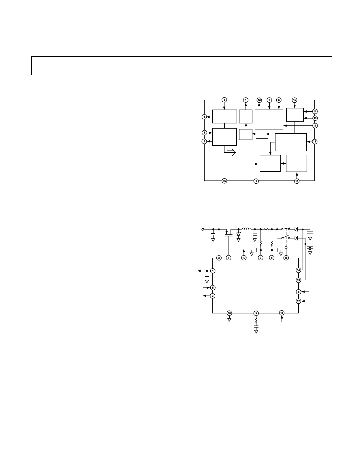
FUNCTIONAL BLOCK DIAGRAM
RESET
VL
SD
LDO +
REFERENCE
SHUTDOWN
RESET
ADP3801/ADP3802
UVLO
+
GND
DRVVCC
GATE
DRIVE
PWM
SD\UVLO
EOC
CURRENT
LOOP
AMP + EOC
COMPARATOR
VOLTAGE
LOOP
COMP
CS+
CS–
FINAL BATTERY
AMP
A/B
A/B
SELECT
MUX
VOLTAGE
PROGRAM
(4.2, 8.4, 12.6)
BATTERY
VOLTAGE
ADJUST
610%
ADJ
BATA
BATB
ISET
PROG
GENERAL DESCRIPTION
The ADP3801 and ADP3802 are complete battery charging
ICs. The devices combine a high accuracy final battery voltage
control with a constant charge current control and an on-board
Low Drop-Out Regulator (LDO). The accuracy of the final
battery voltage control is guaranteed to ±0.75% to safely charge
Li-Ion batteries. An internal multiplexer allows the alternate
charging of two separate battery stacks. The final voltage is pin
programmable to one of three Li-Ion options: 4.2 V (one Li-Ion
cell), 8.4 V (two Li-Ion cells), or 12.6 V (three Li-Ion cells).
Paired with an external microcontroller for charge termination,
the ADP3801/ADP3802 works as a fast charger for NiCad/
NiMH batteries or as a universal charger for all three battery
chemistries. In addition, a pin is provided for changing the final
battery voltage by up to ±10% to adjust for variations in battery
chemistry from different Li-Ion manufacturers without loss of
accuracy in the final battery voltage.
REV. 0
Information furnished by Analog Devices is believed to be accurate and
reliable. However, no responsibility is assumed by Analog Devices for its
use, nor for any infringements of patents or other rights of third parties
which may result from its use. No license is granted by implication or
otherwise under any patent or patent rights of Analog Devices.
One Technology Way, P.O. Box 9106, Norwood, MA 02062-9106, U.S.A.
Tel: 781/329-4700 World Wide Web Site: http://www.analog.com
Fax: 781/326-8703 © Analog Devices, Inc., 1998
Figure 1. 4 Amp Dual Battery Charger

ADP3801/ADP3802–SPECIFICATIONS
(@ –40ⴗC ≤ TA ≤ +85ⴗC, VCC = 10.0 V, unless otherwise noted)
Parameter Conditions Symbol Min Typ Max Units
FINAL BATTERY VOLTAGE
One Li-Ion Cell PROG = VT1, ADJ = VL, T
Two Li-Ion Cells
1
Three Li-Ion Cells
PROG = V
PROG = V
PROG = VT2, ADJ = VL, T
PROG = V
1
PROG = V
PROG = VT3, ADJ = VL, T
PROG = V
PROG = V
, ADJ = VL, –10°C ≤ TA ≤ +70°CV
T1
, ADJ = VL, –40°C ≤ TA ≤ +85°CV
T1
, ADJ = VL, –10°C ≤ TA ≤ +70°CV
T2
, ADJ = VL, –40°C ≤ TA ≤ +85°CV
T2
, ADJ = VL, –10°C ≤ TA ≤ +70°CV
T3
, ADJ = VL, –40°C ≤ TA ≤ +85°CV
T3
= +25°CV
A
= +25°CV
A
= +25°CV
A
BAT
BAT
BAT
BAT
BAT
BAT
BAT
BAT
BAT
4.180 4.200 4.220 V
4.168 4.232 V
4.150 4.250 V
8.366 8.400 8.434 V
8.337 8.463 V
8.300 8.500 V
12.550 12.600 12.650 V
12.505 12.695 V
12.450 12.750 V
BATTERY PROGRAMMING
INPUT (PROG)
One Li-Ion Cell (4.2 V) V
Two Li-Ion Cells (8.4 V) V
Three Li-Ion Cells (12.6 V) V
T1
T2
T3
0.00 0.20 V
1.00 1.20 V
2.05 2.30 V
Fail Safe Voltage (4.2 V) Defaults to 1 Li-Ion Cell 3.10 3.30 V
PROG Input Current I
B
1.5 5 µA
A/B SELECT MUX
Select Battery BATB V
Select Battery BATA V
A/B Input Current I
BATA or BATB Input Resistance Channel Selected R
BATA or BATB Input Current Channel Not Selected I
BATA or BATB Shutdown Current Part in Shutdown IBA, I
2
BATTERY ADJUST INPUT
% of Final Battery Voltage ADJ = 1.0 V, –10°C ≤ T
% of Final Battery Voltage ADJ = 2.3 V, –10°C ≤ T
(ADJ)
≤ +70°C 899091 %
A
≤ +70°C 109 110 111 %
A
IN
BA
IH
IL
IN
, I
2.0 V
0.02 1 µA
185 265 kΩ
BB
BB
0.2 1 µA
0.2 1 µA
0.8 V
ADJ Disable Voltage Threshold 0% Change 2.475 2.6 V
ADJ Bias Current 1.0 V ≤ ADJ ≤ 2.3 V I
B
10 100 nA
OVERVOLTAGE COMPARATOR
Trip Point Percent Above V
BAT
8%
Response Time DRV Goes High tr 2 µs
OSCILLATOR
200 kHz Option (ADP3801) f
500 kHz Option (ADP3802) f
OSC
OSC
150 200 250 kHz
375 500 625 kHz
0% Duty Cycle Threshold @ COMP Pin 1.0 V
100% Duty Cycle Threshold @ COMP Pin 2.0 V
GATE DRIVE
Rise Time CL = 1 nF, VCC – 4 V to 90% t
Fall Time C
Output High Saturation Voltage VCC – V
= 1 nF, 90% to VCC – 4 V t
L
DRV
Output Low Voltage VCC = 8 V V
VCC > 8 V V
r
f
V
OH
OL
OL
1.0 2.0 V
VCC – 7 VCC – 6 V
35 ns
75 ns
275 mV
CURRENT SENSE AMPLIFIER
Input Common-mode Range V
Input Differential Mode Range V
Input Offset Voltage
4
Input Bias Current 0.0 V ≤ V
Input Offset Current 0.0 V ≤ V
Over Current Trip Point V
and V
CS+
3
CS
0.0 V ≤ V
3
CS
CS–
≤ VCC – 2 V V
CSCM
≤ VCC – 2 V V
CSCM
≤ VCC – 2 V V
CSCM
V
CSCM
V
CSDM
CSVOS
CSIB
CSIOS
0.0 VCC – 2 V
0.0 185 mV
1mV
0.3 1 µA
0.01 0.15 µA
185 mV
Response Time DRV Goes High tr 2 µs
ISET INPUT
Charge Current Programming
Function 0.0 V ≤ V
Programming Function Accuracy V
= 1.65 V, –10°C ≤ TA ≤ +70°C–5±1.0 +5 %
ISET
V
= 0.10 V, –10°C ≤ TA ≤ +70°C –25 ±10 +25 %
ISET
ISET Bias Current 0.0 V ≤ V
≤ 1.65 V V
ISET
≤ 1.65 V I
ISET
CS/VISET
B
3
0.1 V/V
15 100 nA
–2–
REV. 0

ADP3801/ADP3802
Parameter Conditions Symbol Min Typ Max Units
BAT
CS+
+ 2 V.
) – (V
5
CS–
3
CS
3
CS
H
L
6
).
0 mA ≤ I
4.1 V ≤ VCC ≤ 20 V, –10°C ≤ T
0 mA ≤ I
4.1 V ≤ VCC ≤ 20 V, –40°C ≤ T
= 10 mA V
LOAD
LOAD
LOAD
≤ 10 mA,
≤ 10 mA,
≤ +70°C VL 3.267 3.3 3.333 V
A
≤ +85°C VL 3.250 3.350 V
A
≥ 95% of the final battery voltage.
BAT
DO
VL
SYON
SYOFF
2.0 V
10 20 mA
10 mV
0.2 mV
0.8 V
0.4 0.8 V
5.0 7.0 mA
115 180 µA
EOC OUTPUT
Trip Point 100 kΩ to VL V
Hysteresis 100 kΩ to VL V
SHUTDOWN (SD)
ON SD
OFF SD
SD Input Current 0.2 1 µA
LOW DROPOUT REGULATOR
Output Voltage
Dropout Voltage (VCC – VL) I
Output Current Drive I
RESET OUTPUT
VL Rising Threshold RESET High 2.5 2.7 2.9 V
VL Falling Threshold RESET Low 2.4 2.55 2.8 V
Output High Logic Level 1 MΩ to Ground External 2.4 2.9 V
POWER SUPPLY
ON Supply Current No External Loads I
OFF Supply Current No External Loads I
6, 7
UVLO
VCC Rising Threshold Turn On 3.8 3.9 4.0 V
VCC Falling Threshold Turn Off, IVL = 1 mA 3.4 V
NOTES
1
VCC = V
2
See Figure 5.
3
VCS = (V
4
Accuracy guaranteed by ISET INPUT, Programming Function Accuracy specification.
5
EOC Output Comparator monitors charge current, and it is enabled when V
6
LDO is active during SD and UVLO.
7
Turn-off threshold depends on LDO dropout.
All limits at temperature extremes are guaranteed via correlation using standard Statistical Quality Control (SQC) methods.
Specifications subject to change without notice.
–3–REV. 0

ADP3801/ADP3802
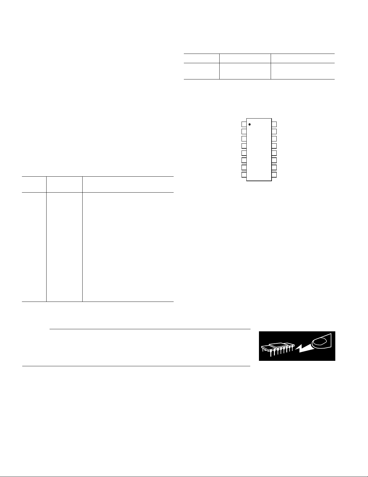
TOP VIEW
(Not to Scale)
16
15
14
13
12
11
10
9
1
2
3
4
5
6
7
8
DRV
VL
SD
CS–
CS+
ISET
GND
A/B
BATA
BATB
PROG
ADJ
EOC
COMP
ADP3801
ADP3802
VCC
RESET
WARNING!
ESD SENSITIVE DEVICE
ABSOLUTE MAXIMUM RATINGS*
Input Voltage (VCC to GND) . . . . . . . . . . . . . . –0.3 V to 20 V
DRV, V
CS+
, V
to GND . . . . . . . . . . . . . . . . –0.3 V to VCC
CS–
BATA, BATB to GND . . . . . . . . . . . . . . . . . –0.3 V to 14.0 V
A/B, ISET, PROG, ADJ to GND . . . . . . . . . . . –0.3 V to VL
SD, RESET, COMP, EOC to GND . . . . . . . . . . –0.3 V to VL
Power Dissipation . . . . . . . . . . . . . . . . . . . . Internally Limited
θJA . . . . . . . . . . . . . . . . . . . . . . . . . . . . . . . . . . . . . 75°C/W
Ambient Temperature Range . . . . . . . . . . . . –40°C to +85°C
Storage Temperature Range . . . . . . . . . . . . –65°C to +150°C
Lead Temperature Range (Soldering 10 sec) . . . . . . . +300°C
NOTES
*This is a stress rating only and functional operation of the device at these or any
other conditions above those indicated in the operation section of this specification
is not implied. Exposure to absolute maximum rating conditions for extended
periods may affect device reliability.
θ
is specified for worst case conditions with device soldered on a circuit board.
JA
PIN FUNCTION DESCRIPTIONS
Pin
Number Mnemonic Function
1 DRV External Transistor Drive
2 RESET Power on RESET Output
3 VCC Supply Voltage
4 VL LDO Output
5 SD Shutdown Control Input
6 CS– Negative Current Sense Input
7 CS+ Positive Current Sense Input
8 ISET Charge Current Program Input
9 COMP External Compensation Node
10 EOC End-of-Charge Output Signal
11 ADJ Adjust Battery Voltage ±
10%
12 PROG Program Final Battery Voltage Input
13 BATB Battery “B” Voltage Sense
14 BATA Battery “A” Voltage Sense
15 A/B
1
“A” or “B” Battery Select Input
16 GND Ground
NOTE
1
“L” = Battery “A.”
ORDERING GUIDE
Model Package Option Oscillator Frequency
ADP3801AR R-16A 200 kHz
ADP3802AR R-16A 500 kHz
PIN CONFIGURATION
CAUTION
ESD (electrostatic discharge) sensitive device. Electrostatic charges as high as 4000 V readily
accumulate on the human body and test equipment and can discharge without detection. Although
the ADP3801/ADP3802 features proprietary ESD protection circuitry, permanent damage may
occur on devices subjected to high energy electrostatic discharges. Therefore, proper ESD precautions are recommended to avoid performance degradation or loss of functionality.
–4–
REV. 0

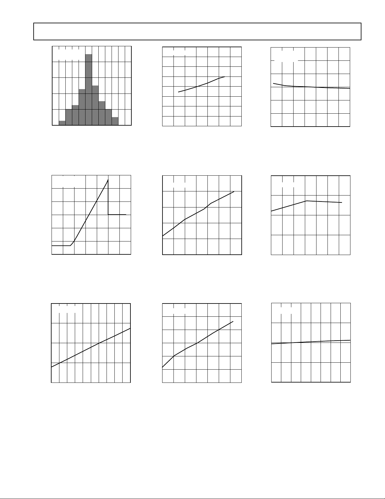
Typical Performance Characteristics–ADP3801/ADP3802
SUPPLY VOLTAGE – Volts
LDO ACCURACY – %
4681012 1618
0
0.1
0.2
14 20
TA = +258C
–0.2
–0.1
100
VCC = 10V
= +258C
T
A
80
60
40
20
TOTAL NUMBEROF PARTS
0
–0.3
–0.5
–0.4
–0.2 0 0.2 0.4 0.6
V
Figure 2. V
15
10
5
0
–5
PERCENT CHANGE – %
BAT
V
–10
BAT
VCC = 10V
T
= +258C
A
–0.1
0.1 0.3 0.5
ACCURACY – %
BAT
Accuracy Distribution
0.4
VCC = 10V
0.3
0.2
0.1
0
ACCURACY – %
–0.1
BAT
V
–0.2
–0.3
–0.4
–40
Figure 3. V
Temperature
10
9
8
7
THRESHOLD – %
6
–20 0 20 40 60 80 100
TEMPERATURE – 8C
Accuracy vs.
BAT
VCC = 10V
0.3
TA = +258C
V
= 4.2V
BAT
0.2
0.1
0
ACCURACY – %
–0.1
BAT
V
–0.2
–0.3
6 8 10 12 14 18 20
SUPPLY VOLTAGE – Volts
Figure 4. V
Accuracy vs. Supply
BAT
16
Voltage
200
VCC = 10V
195
190
THRESHOLD – mV
185
–15
0 0.5 1.0 1.5 2.0 3.0 3.5
Figure 5. V
3.7
TA = +258C
3.6
3.5
3.4
UVLO TRIP POINT – Votts
3.3
01234 67
V
ADJ
Percent Change vs. V
BAT
LDO LOAD CURRENT – mA
2.5
– Volts
58910
Figure 8. UVLO Trip Point-Off vs.
LDO Load Current
ADJ
5
–40 –20 0 20 40 80 100
TEMPERATURE – 8C
60
Figure 6. Overvoltage Comparator
Threshold vs. Temperature
0.3
VCC = 10V
0.2
0.1
0
–0.1
LDO ACCURACY – %
–0.2
–0.3
–40
–20 0 20 40 60 80 100
TEMPERATURE – 8C
Figure 9. LDO Accuracy vs.
Temperature
180
–40 –20 0 20 40 80 100
TEMPERATURE – 8C
60
Figure 7. Overcurrent Comparator
Threshold vs. Temperature
Figure 10. LDO Accuracy vs. Supply
Voltage
–5–REV. 0

ADP3801/ADP3802
SATURATION VOLTAGE – Volts
–40 –20
40 60 80
0
0.2
100
VCC = 10V
200
0.4
0.3
TEMPERATURE – 8C
0.4
TA = +258C
0.3
0.2
DROPOUT VOLTAGE – Volts
0.1
01234 6758
LOAD CURRENT – mA
910
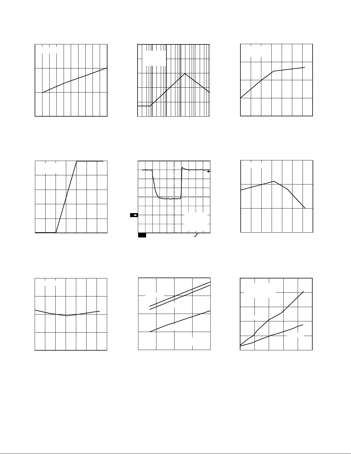
Figure 11. LDO Dropout Voltage vs.
Load Current
100
VCC = 10V
TA = +258C
80
60
40
DUTY CYCLE – %
20
0
0
0.5 2.0 2.5 3.0
V
1.51.0
COMP
– Volts
3.5
Figure 14. Duty Cycle vs. COMP Pin
Voltage
0
VCC = 10V
= +258C
T
A
–20
–40
–60
PSRR – dB
–80
–100
1.0E+01
= 1mF
C
LDO
1.0E+03 1.0E+04 1.0E+05 1.0E+06
1.0E+02
FREQUENCY – Hz
Figure 12. LDO PSRR vs. Frequency
12
10
8
6
4
DRV – Volts
2
0
1
2.00V
CH1
TIME – ns
VCC = 10V
= 1nF
C
L
T
= +258C
A
250ns/DIV
Figure 15. DRV Rise and Fall Times
215
ADP3801
VCC = 10V
205
195
FREQUENCY – kHz
185
175
–40 –20
0 20 40 80 10060
TEMPERATURE – 8C
Figure 13. Oscillator Frequency vs.
Temperature
9.40VCH1M 250ns
Figure 16. DRV High Saturation Voltage vs. Temperature
3.9
VCC = 10V
3.8
3.7
3.6
CLAMP VOLTAGE – Volts
3.5
–40 –20
Figure 17. DRV Output Low Voltage
with VCC = 10 V vs. Temperature
40 60 80
200
TEMPERATURE – 8C
5.5
TA = +858C
5.0
TA = +258C
4.5
TA = –408C
NOT SWITCHING
SD = ON
12
100
4.0
POWER SUPPLY CURRENT – mA
3.5
48 16
SUPPLY VOLTAGE – Volts
Figure 18. Power Supply Current vs.
Supply Voltage @ Three Temperatures
–6–
15
VCC = 10V
= +258C
T
A
13
50% DUTY CYCLE
11
ADP3802
9
7
POWER SUPPLY CURRENT – mA
20
5
0 0.5 1.5
CAPACITIVE LOAD – nF
ADP3801
2.01.0
2.5
Figure 19. Power Supply Current vs.
Capacitive Load on DRV
REV. 0
 Loading...