High Speed, Dual,
FEATURES
Industry-standard-compatible pinout
High current drive capability
Precise UVLO comparator with hysteresis
3.3 V-compatible inputs
10 ns typical rise time and fall time at 2.2 nF load
Matched propagation delays between channels
Fast propagation delay
4.5 V to 18 V supply voltage
Parallelable dual outputs
Rated from −40°C to +125°C junction temperature
Thermally enhanced packages, 8-lead SOIC_N_EP and 8-lead
MINI_SO_EP
APPLICATIONS
AC-to-dc switch mode power supplies
DC-to-dc power supplies
Synchronous rectification
Motor drives
4 A MOSFET Driver
ADP3654
GENERAL DESCRIPTION
The ADP3654 high current and dual high speed driver is capable
of driving two independent N-channel power MOSFETs. The
driver uses the industry-standard footprint but adds high speed
switching performance.
The wide input voltage range allows the driver to be compatible
with both analog and digital PWM controllers.
Digital power controllers are powered from a low voltage
supply, and the driver is powered from a higher voltage supply.
The ADP3654 driver adds UVLO and hysteresis functions,
allowing safe startup and shutdown of the higher voltage supply
when used with low voltage digital controllers.
The driver is available in thermally enhanced SOIC_N_EP and
MINI_SO_EP packaging to maximize high frequency and
current switching in a small printed circuit board (PCB) area.
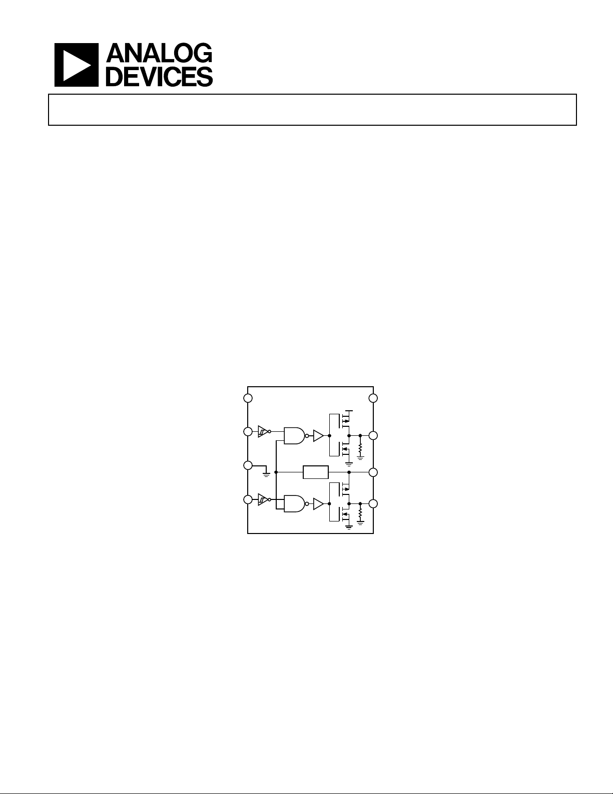
FUNCTIONAL BLOCK DIAGRAM
1
NC
INA
PGND
INB
2
3
4
ADP3654
UVLO
Figure 1.
8
7
6
5
NC
OUTA
VDD
OUTB
09054-001
V
DD
Rev. 0
Information furnished by Analog Devices is believed to be accurate and reliable. However, no
responsibility is assumed by Anal og Devices for its use, nor for any infringements of patents or ot her
rights of third parties that may result from its use. Specifications subject to change without notice. No
license is granted by implication or otherwise under any patent or patent rights of Analog Devices.
Trademarks and registered trademarks are the property of their respective owners.
One Technology Way, P.O. Box 9106, Norwood, MA 02062-9106, U.S.A.
Tel: 781.329.4700 www.analog.com
Fax: 781.461.3113 ©2010 Analog Devices, Inc. All rights reserved.

ADP3654
TABLE OF CONTENTS
Features.............................................................................................. 1
Applications....................................................................................... 1
General Description ......................................................................... 1
Functional Block Diagram .............................................................. 1
Revision History ............................................................................... 2
Specifications..................................................................................... 3
Timing Diagrams.......................................................................... 3
Absolute Maximum Ratings............................................................ 4
ESD Caution.................................................................................. 4
Pin Configuration and Function Descriptions............................. 5
Typical Performance Characteristics ............................................. 6
REVISION HISTORY
8/10—Revision 0: Initial Version
Test Circuit .........................................................................................8
Theory of Operation .........................................................................9
Input Drive Requirements (INA and INB)................................9
Low-Side Drivers (OUTA, OUTB).............................................9
Supply Capacitor Selection ..........................................................9
PCB Layout Considerations.........................................................9
Parallel Operation ...................................................................... 10
Thermal Considerations............................................................ 10
Outline Dimensions....................................................................... 12
Ordering Guide .......................................................................... 12
Rev. 0 | Page 2 of 12

ADP3654
SPECIFICATIONS
VDD = 12 V, TJ = −40°C to +125°C, unless otherwise noted.1
Table 1.
Parameter Symbol Test Conditions/Comments Min Typ Max Unit
SUPPLY
Supply Voltage Range V
DD
Supply Current IDD No switching 1.2 3 mA
UVLO
Turn-On Threshold Voltage V
Turn-Off Threshold Voltage V
UVLO_ON
UVLO_OFF
Hysteresis 0.3 V
DIGITAL INPUTS (INA, INB)
Input Voltage High VIH See Figure 2 2.0 V
Input Voltage Low VIL See Figure 2 0.8 V
Input Current IIN 0 V < VIN < VDD −20 +20 μA
Internal Pull-Up/Pull-Down Current 6 μA
OUTPUTS (OUTA, OUTB)
Output Resistance, Unbiased VDD = PGND 80 kΩ
Peak Source Current See Figure 14 4 A
Peak Sink Current See Figure 14 −4 A
SWITCHING TIME
OUTA and OUTB Rise Time t
OUTA and OUTB Fall Time t
OUTA and OUTB Rising Propagation Delay t
OUTA and OUTB Falling Propagation Delay t
RISE
FALL
D1
D2
Delay Matching Between Channels 2 ns
1
All limits at temperature extremes guaranteed via correlation using standard statistical quality control (SQC) methods.
4.5 18 V
VDD rising, TJ = 25°C, see Figure 3 3.8 4.2 4.5 V
VDD falling, TJ = 25°C, see Figure 3 3.5 3.9 4.3 V
C
= 2.2 nF, see Figure 2 10 25 ns
LOAD
C
= 2.2 nF, see Figure 2 10 25 ns
LOAD
C
= 2.2 nF, see Figure 2 14 30 ns
LOAD
C
= 2.2 nF, see Figure 2 22 35 ns
LOAD
TIMING DIAGRAMS
INA,
INB
OUTA,
OUTB
V
IH
t
10%
V
UVLO_ON
V
UVLO_OFF
V
DD
OUTPUTS DISABLED
D1tRISE
90%
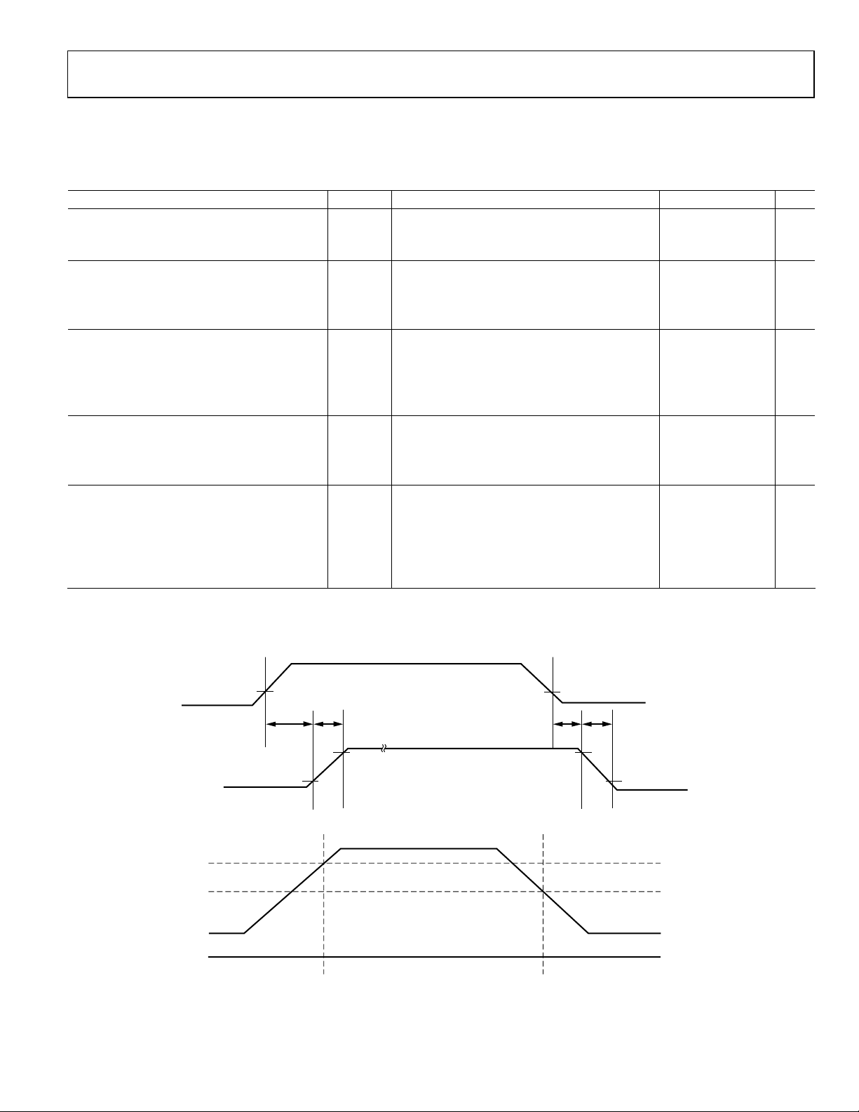
Figure 2. Output Timing Diagram
NORMAL OP E RATIONUVLO MO DE
Figure 3. UVLO Function
V
IL
tD2t
FALL
90%
UVLO MO DE
OUTPUTS DISABLED
10%
09054-002
9054-003
Rev. 0 | Page 3 of 12

ADP3654
ABSOLUTE MAXIMUM RATINGS
Table 2.
Parameter Rating
VDD −0.3 V to +20 V
OUTA, OUTB
DC −0.3 V to VDD + 0.3 V
<200 ns −2 V to VDD + 0.3 V
INA, INB −0.3 V to VDD + 0.3 V
ESD
Human Body Model (HBM) 3.5 kV
Field Induced Charged Device Model
(FICDM)
SOIC_N_EP 1.5 kV
MINI_SO_EP 1.0 kV
θJA, JEDEC 4-Layer Board
SOIC_N_EP1 59°C/W
MINI_SO_EP1 43°C/W
Junction Temperature Range −40°C to +150°C
Storage Temperature Range −65°C to +150°C
Lead Temperature
Soldering (10 sec) 300°C
Vapor Phase (60 sec) 215°C
Infrared (15 sec) 260°C
1
θJA is measured per JEDEC standards, JESD51-2, JESD51-5, and JESD51-7, as
appropriate with the exposed pad soldered to the PCB.
Stresses above those listed under Absolute Maximum Ratings
may cause permanent damage to the device. This is a stress
rating only; functional operation of the device at these or any
other conditions above those indicated in the operational
section of this specification is not implied. Exposure to absolute
maximum rating conditions for extended periods may affect
device reliability.
ESD CAUTION
Rev. 0 | Page 4 of 12
 Loading...