Dual, Bootstrapped, 12 V MOSFET
V
FEATURES
All-in-one synchronous buck driver
Bootstrapped high-side drive
One PWM signal generates both drives
Anti-crossconduction protection circuitry
for disabling the driver outputs
OD
APPLICATIONS
Telecom and datacom networking
Industrial and medical systems
Point of load conversion: memory, DSP, FPGA, ASIC
Driver with Output Disable
ADP3650
GENERAL DESCRIPTION
The ADP3650 is a dual, high voltage MOSFET driver optimized
for driving two N-channel MOSFETs, the two switches in a
nonisolated synchronous buck power converter. Each driver is
capable of driving a 3000 pF load with a 45 ns propagation delay
and a 25 ns transition time. One of the drivers can be bootstrapped and is designed to handle the high voltage slew rate
associated with floating high-side gate drivers. The ADP3650
includes overlapping drive protection to prevent shoot-through
current in the external MOSFETs.
The
MOSFETs to prevent rapid output capacitor discharge during
system shutdown.
The ADP3650 is specified over the temperature range of −40°C
to +85°C and is available in 8-lead SOIC_N and 8-lead LFCSP_VD
packages.
pin shuts off both the high-side and the low-side
OD
OD
IN
2
3
ADP3650
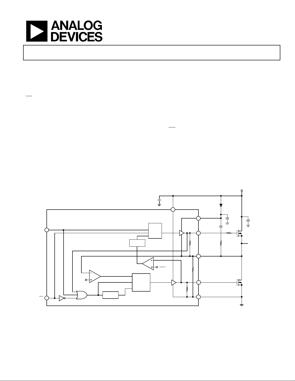
FUNCTIONAL BLOCK DIAGRAM
12
C
BST1
D1
C
BST2
R
G
R
BST
Q1
TO
INDUCTOR
Q2
7826-001
VCC
4
BST
1
LATCH
R1
R2
Q
S
DELAY
CMP
VCC
6
CMP
1V
DELAY
CONTROL
LOGIC
8
7
5
6
DRVH
SW
DRVL
PGND
Figure 1.
Rev. A
Information furnished by Analog Devices is believed to be accurate and reliable. However, no
responsibility is assumed by Analog Devices for its use, nor for any infringements of patents or other
rights of third parties that may result from its use. Specifications subject to change without notice. No
license is granted by implication or otherwise under any patent or patent rights of Analog Devices.
Trademarks and registered trademarks are the property of their respective owners.
One Technology Way, P.O. Box 9106, Norwood, MA 02062-9106, U.S.A.
Tel: 781.329.4700 www.analog.com
Fax: 781.461.3113 ©2008–2010 Analog Devices, Inc. All rights reserved.

ADP3650
TABLE OF CONTENTS
Features .............................................................................................. 1
Applications ....................................................................................... 1
General Description ......................................................................... 1
Functional Block Diagram .............................................................. 1
Revision History ............................................................................... 2
Specifications ..................................................................................... 3
Timing Characteristics ................................................................ 4
Absolute Maximum Ratings ............................................................ 5
Thermal Resistance ...................................................................... 5
ESD Caution .................................................................................. 5
Pin Configurations and Function Descriptions ........................... 6
Typical Performance Characteristics ............................................. 7
Theory of Operation ........................................................................ 9
REVISION HISTORY
7/10—Rev. 0 to Rev. A
Changes to General Description Section ...................................... 1
Changes to Table 1 ............................................................................ 3
Changes to Operating Ambient Temperature Range Parameter,
Table 2 ................................................................................................ 5
Changes to Figure 8 and Figure 9 ................................................... 7
Changes to Ordering Guide .......................................................... 12
10/08—Revision 0: Initial Version
Low-Side Driver ............................................................................9
High-Side Driver ...........................................................................9
Overlap Protection Circuit ...........................................................9
Applications Information .............................................................. 10
Supply Capacitor Selection ....................................................... 10
Bootstrap Circuit ........................................................................ 10
MOSFET Selection ..................................................................... 10
High-Side (Control) MOSFETs ................................................ 10
Low-Side (Synchronous) MOSFETs ........................................ 11
PCB Layout Considerations ...................................................... 11
Outline Dimensions ....................................................................... 12
Ordering Guide .......................................................................... 12
Rev. A | Page 2 of 12

ADP3650
SPECIFICATIONS
VCC = 12 V, BST = 4 V to 26 V, TA = −40°C to +85°C, unless otherwise noted.1
Table 1.
Parameter Symbol Test Conditions/Comments Min Typ Max Unit
DIGITAL INPUTS (IN, OD)
Input Voltage High 2.0 V
Input Voltage Low 0.8 V
Input Current −1 +1 μA
Hysteresis 40 250 350 mV
HIGH-SIDE DRIVER
Output Resistance, Sourcing Current BST − SW = 12 V; TA = 25°C 3.3 Ω
BST − SW = 12 V; TA = −40°C to +85°C 2.5 3.9 Ω
Output Resistance, Sinking Current BST − SW = 12 V; TA = 25°C 1.8 Ω
BST − SW = 12 V; TA = −40°C to +85°C 1.4 2.6 Ω
Output Resistance, Unbiased BST − SW = 0 V 10 kΩ
Transition Times t
t
Propagation Delay Times t
25°C ≤ TA ≤ 85°C, see Figure 3
t
SW Pull-Down Resistance SW to PGND 10 kΩ
LOW-SIDE DRIVER
Output Resistance, Sourcing Current TA = 25°C 3.3 Ω
T
Output Resistance, Sinking Current TA = 25°C 1.8 Ω
T
Output Resistance, Unbiased VCC = PGND 10 kΩ
Transition Times t
t
Propagation Delay Times t
t
Timeout Delay SW = 5 V 110 190 ns
SW = PGND 95 150 ns
SUPPLY
Supply Voltage Range V
Supply Current I
UVLO Voltage VCC rising 1.5 3.0 V
Hysteresis 350 mV
1
All limits at temperature extremes are guaranteed via correlation using standard statistical quality control (SQC) methods.
rDRVH
fDRVH
pdhDRVH
pdlDRVH
t
pdl
OD
t
pdh
OD
rDRVL
fDRVL
pdhDRVL
pdlDRVL
t
pdl
OD
t
pdh
OD
CC
BST = 12 V, IN = 0 V 2 5 mA
SYS
BST − SW = 12 V, C
BST − SW = 12 V, C
BST − SW = 12 V, C
BST − SW = 12 V, C
See Figure 2 20 35 ns
See Figure 2 40 55 ns
= −40°C to +85°C 2.4 3.9 Ω
A
= −40°C to +85°C 1.4 2.6 Ω
A
C
= 3 nF, see Figure 3 20 35 ns
LOAD
C
= 3 nF, see Figure 3 16 30 ns
LOAD
C
= 3 nF, see Figure 3 12 35 ns
LOAD
C
= 3 nF, see Figure 3 30 45 ns
LOAD
See Figure 2 20 35 ns
See Figure 2 110 190 ns
4.15 13.2 V
= 3 nF, see Figure 3 25 40 ns
LOAD
= 3 nF, see Figure 3 20 30 ns
LOAD
= 3 nF, 32 45 70 ns
LOAD
= 3 nF, see Figure 3 25 35 ns
LOAD
Rev. A | Page 3 of 12

ADP3650
TIMING CHARACTERISTICS
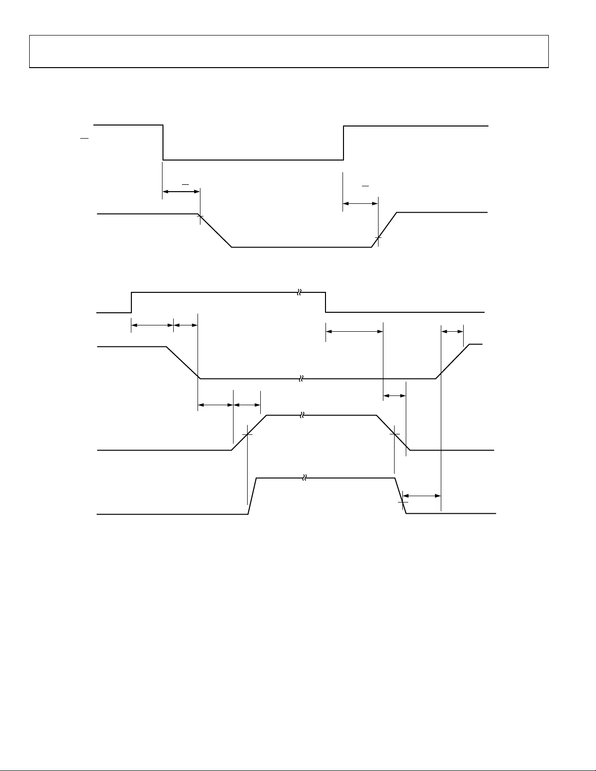
Timing is referenced to the 90% and 10% points, unless otherwise noted.
OD
t
pdlOD
t
pdhOD
DRVH
OR
DRVL
90%
10%
7826-004
Figure 2. Output Disable Timing Diagram
IN
t
DRVL
DRVH
TO
SW
SW
pdlDRVLtfDRVL
t
pdhDRVHtrDRVH
V
TH
t
pdlDRVH
t
rDRVL
t
fDRVH
V
TH
t
pdhDRVL
1V
07826-005
Figure 3. Timing Diagram
Rev. A | Page 4 of 12
 Loading...