High Speed, Dual, 2 A MOSFET Driver
FEATURES
Industry-standard-compatible pinout
High current drive capability
Precise threshold shutdown comparator
UVLO with hysteresis
Overtemperature warning signal
Overtemperature shutdown
3.3 V-compatible inputs
Rise time and fall time: 10 ns typical at 2.2 nF load
Fast propagation delay
Matched propagation delays between channels
Supply voltage: 9.5 V to 18 V
Dual outputs can be operated in parallel
(ADP3629/ADP3630)
Rated from −40°C to +85°C ambient temperature
8-lead SOIC_N and 8-lead MSOP
APPLICATIONS
AC-to-DC switch mode power supplies
DC-to-DC power supplies
Synchronous rectification
Motor drives
ADP3629/ADP3630/ADP3631
GENERAL DESCRIPTION
The ADP3629/ADP3630/ADP3631 are dual, high current, high
speed drivers, capable of driving two independent N-channel
power MOSFETs. The ADP3629/ADP3630/ADP3631 use the
industry-standard footprint but add high speed switching performance and improved system reliability.
The ADP3629/ADP3630/ADP3631 have an internal temperature
sensor and provide two levels of overtemperature protection: an
overtemperature warning and an overtemperature shutdown at
extreme junction temperatures.
The SD function, generated from a precise internal comparator,
provides fast system enable or shutdown. This feature allows
redundant overvoltage protection, complementing the protection inside the main controller device, or provides safe system
shutdown in the event of an overtemperature warning.
The wide input voltage range allows the driver to be compatible
with both analog and digital PWM controllers.
Digital power controllers are supplied from a low voltage supply,
and the driver is supplied from a higher voltage supply. The
ADP3629/ADP3630/ADP3631 add UVLO and hysteresis functions, allowing safe startup and shutdown of the higher voltage
supply when used with low voltage digital controllers.
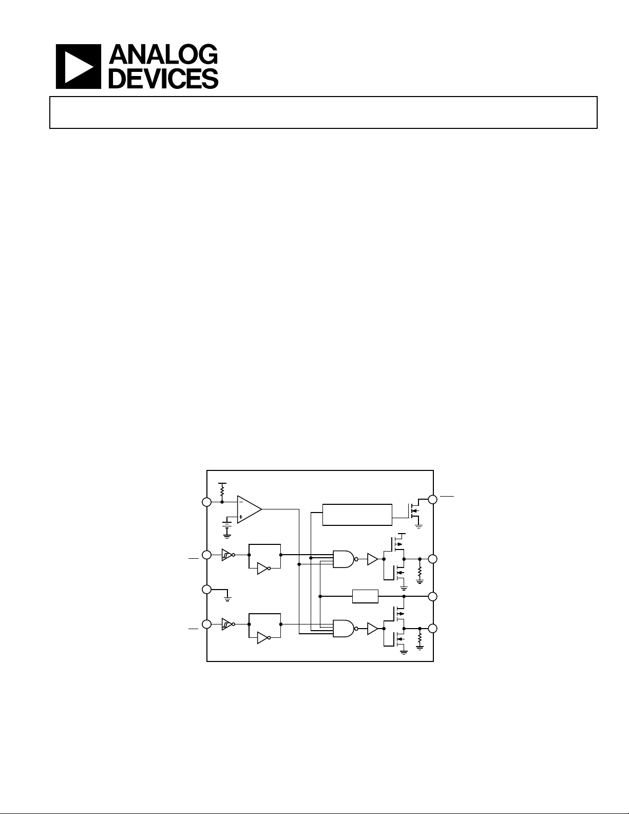
FUNCTIONAL BLOCK DIAGRAM
V
DD
1
SD
V
EN
NONINVERTING
2
INA,
INA
3
PGND
4
INB,
INB
Rev. 0
Information furnished by Analog Devices is believed to be accurate and reliable. However, no
responsibility is assumed by Analog Devices for its use, nor for any infringements of patents or other
rights of third parties that may result from its use. Specifications subject to change without notice. No
license is granted by implication or otherwise under any patent or patent rights of Analog Devices.
Trademarks and registered trademarks are the property of their respective owners.
INVERTING
NONINVERTING
INVERTING
ADP3629/ADP3630/ADP3631
8
OTW
OVERTEMPERATURE
PROTECTION
UVLO
Figure 1.
One Technology Way, P.O. Box 9106, Norwood, MA 02062-9106, U.S.A.
Tel: 781.329.4700 www.analog.com
Fax: 781.461.3113 ©2009 Analog Devices, Inc. All rights reserved.
V
DD
7
OUTA
6
VDD
5
OUTB
08401-101

ADP3629/ADP3630/ADP3631
TABLE OF CONTENTS
Features .............................................................................................. 1
Applications ....................................................................................... 1
General Description ......................................................................... 1
Functional Block Diagram .............................................................. 1
Revision History ............................................................................... 2
Specifications ..................................................................................... 3
Timing Diagrams .......................................................................... 4
Absolute Maximum Ratings ............................................................ 6
Thermal Resistance ...................................................................... 6
ESD Caution .................................................................................. 6
Pin Configurations and Function Descriptions ........................... 7
Typical Performance Characteristics ............................................. 8
REVISION HISTORY
9/09—Revision 0: Initial Version
Test Circuit ...................................................................................... 10
Theory of Operation ...................................................................... 11
Input Drive Requirements (INA,
Low-Side Drivers (OUTA, OUTB) .......................................... 11
Shutdown (SD) Function .......................................................... 11
Overtemperature Protections ................................................... 12
Supply Capacitor Selection ....................................................... 12
PCB Layout Considerations ...................................................... 12
Parallel Operation ...................................................................... 12
Thermal Considerations ............................................................ 13
Outline Dimensions ....................................................................... 14
Ordering Guide .......................................................................... 14
INA
, INB,
INB
, and SD) .. 11
Rev. 0 | Page 2 of 16

ADP3629/ADP3630/ADP3631
SPECIFICATIONS
VDD = 12 V, TJ = −40°C to +125°C, unless otherwise noted.1
Table 1.
Parameter Symbol Test Conditions/Comments Min Typ Max Unit
SUPPLY
Supply Voltage Range V
DD
Supply Current IDD
Standby Current I
SD = 5 V 1.2 3 mA
SBY
UVLO
Turn-On Threshold Voltage V
Turn-Off Threshold Voltage V
UVLO_ON
UVLO_OFF
Hysteresis 1.0 V
DIGITAL INPUTS (INA, INA, INB, INB, SD)
Input Voltage High VIH 2.0 V
Input Voltage Low VIL 0.8 V
Input Current IIN 0 V < VIN < VDD −20 +20 μA
SD Threshold High V
SD_H
T
SD Threshold Low V
SD Hysteresis V
SD_L
SD_HYST
Internal Pull-Up/Pull-Down Current 6 μA
OUTPUTS (OUTA, OUTB)
Output Resistance, Unbiased VDD = PGND 80 kΩ
Peak Source Current See Figure 20 2 A
Peak Sink Current See Figure 20 −2 A
SWITCHING TIME
OUTA, OUTB Rise Time t
OUTA, OUTB Fall Time t
OUTA, OUTB Rising Propagation Delay t
OUTA, OUTB Falling Propagation Delay t
SD Propagation Delay Low t
SD Propagation Delay High t
RISE
FALL
D1
D2
dL_SD
dH_SD
Delay Matching Between Channels 2 ns
OVERTEMPERATURE PROTECTION
Overtemperature Warning Threshold TW See Figure 6 120 135 150 °C
Overtemperature Shutdown Threshold TSD See Figure 6 150 165 180 °C
Temperature Hysteresis for Shutdown T
Temperature Hysteresis for Warning T
Overtemperature Warning Low V
1
All limits at temperature extremes guaranteed via correlation using standard statistical quality control (SQC) methods.
HYS_SD
HYS_W
OTW_O L
9.5 18 V
No switching, INA, INA
, INB, and INB
1.2 3 mA
disabled
VDD rising, TA = 25°C 8.0 8.7 9.5 V
VDD falling, TA = 25°C 7.0 7.7 8.5 V
1.19 1.28 1.38 V
= 25°C 1.21 1.28 1.35 V
A
T
= 25°C 0.95 1.0 1.05 V
A
TA = 25°C 240 280 320 mV
C
= 2.2 nF, see Figure 3 and Figure 4 10 25 ns
LOAD
C
= 2.2 nF, see Figure 3 and Figure 4 10 25 ns
LOAD
C
= 2.2 nF, see Figure 3 and Figure 4 14 30 ns
LOAD
C
= 2.2 nF, see Figure 3 and Figure 4 22 35 ns
LOAD
See Figure 2 32 45 ns
See Figure 2 48 75 ns
See Figure 6 30 °C
See Figure 6 10 °C
Open drain, −500 μA 0.4 V
Rev. 0 | Page 3 of 16

ADP3629/ADP3630/ADP3631
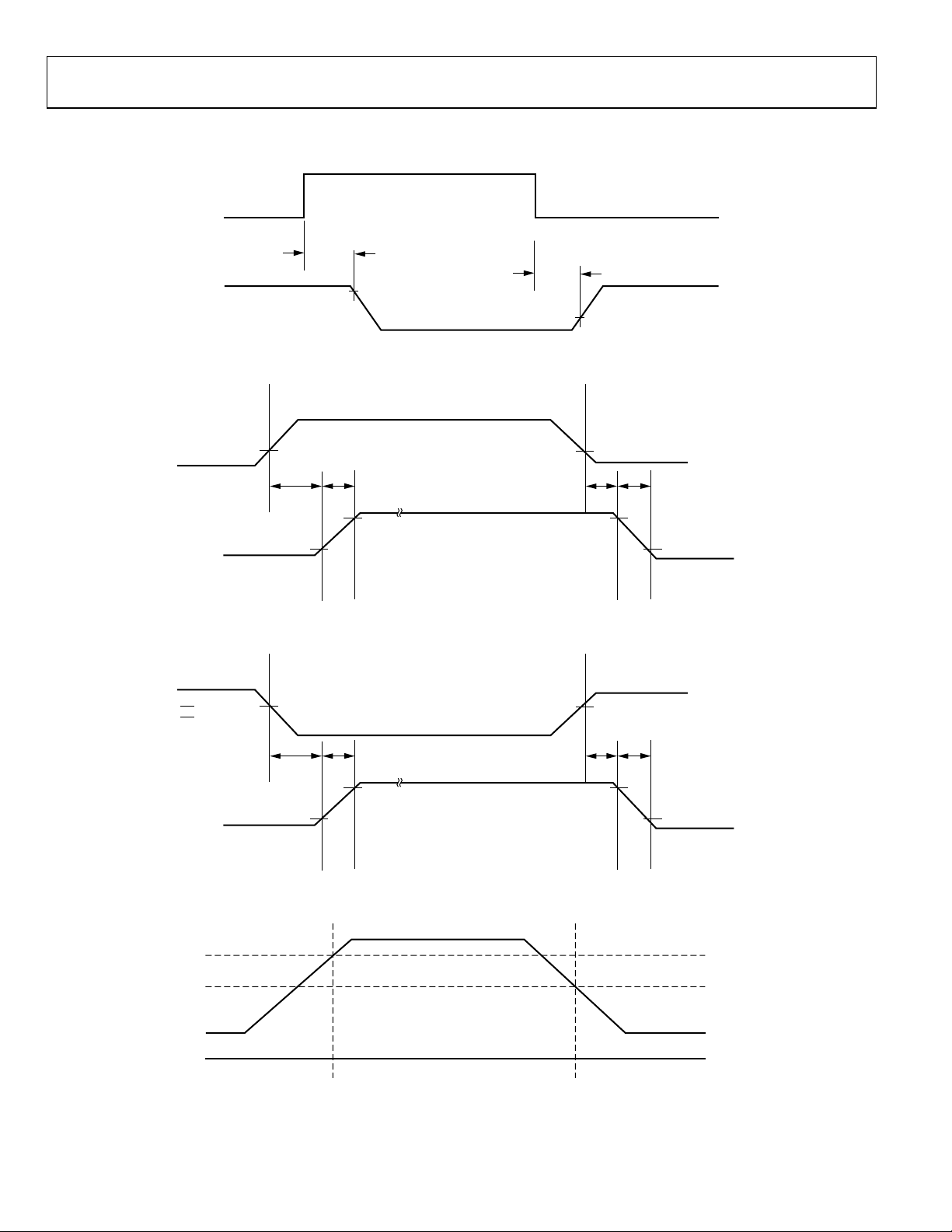
TIMING DIAGRAMS
SD
t
dL_SD
t
dH_SD
OUTA,
OUTB
90%
Figure 2. Shutdown Timing Diagram
10%
08401-002
INA,
INB
OUTA,
OUTB
V
IH
t
D1tRISE
90%
10%
V
IL
tD2t
FALL
90%
10%
08401-003
Figure 3. Output Timing Diagram (Noninverting)
INA,
INB
OUTA,
OUTB
V
IL
t
D1tRISE
90%
10%
Figure 4. Output Timing Diagram (Inverting)
V
IH
tD2t
FALL
90%
10%
08401-103
V
UVLO_ON
V
UVLO_OFF
V
DD
NORMAL OPERATIONUVLO MODE
OUTPUTS DI SABL E D
UVLO MODE
OUTPUTS DI S ABLED
8401-005
Figure 5. UVLO Function
Rev. 0 | Page 4 of 16

ADP3629/ADP3630/ADP3631
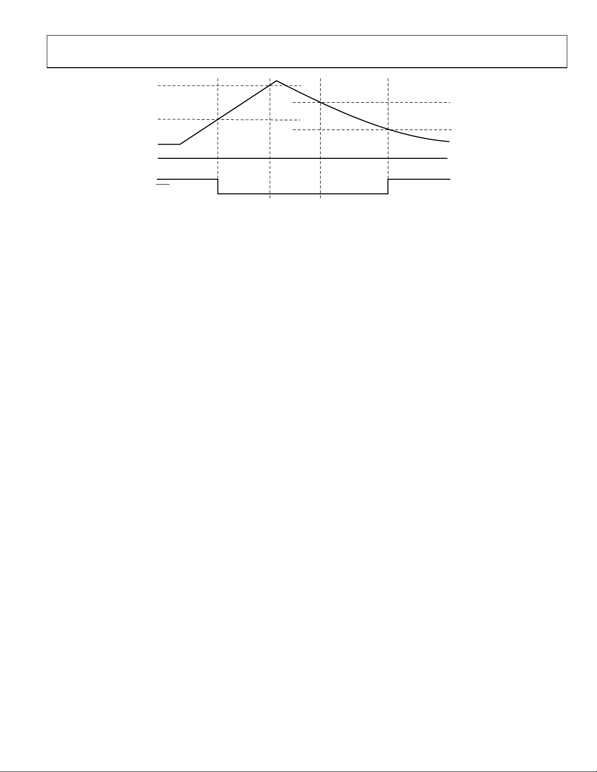
T
SD
T
–
T
SD
HYS_SD
T
W
T
J
NORMAL OPERATION NORMAL OPERATION
OTW
OT WARNING
OUTPUTS
ENABLED
OT SHUTDO WN
OUTPUTS
DISABLED
OT WARNING
OUTPUTS
ENABLED
T
–
T
W
HYS_W
08401-006
Figure 6. Overtemperature Warning and Shutdown
Rev. 0 | Page 5 of 16
 Loading...