

High Speed, Dual, 4 A MOSFET Driver
ADP3623/ADP3624/ADP3625/ADP3633/ADP3634/ADP3635
1
8
2
7
3
6
4
5
OVERTEMPERATURE
PROTECTION
NONINVERTING
INA,
INA
PGND
INB,
INB
SD
OUTA
VDD
OUTB
OTW
V
DD
V
DD
INVERTING
NONINVERTING
INVERTING
UVLO
V
EN
08132-101
ADP3623/ADP3624/ADP3625
ADP3633/ADP3634/ADP3635
FEATURES
Industry-standard-compatible pinout
High current drive capability
Precise threshold shutdown comparator
UVLO with hysteresis
Overtemperature warning signal
Overtemperature shutdown
3.3 V-compatible inputs
10 ns typical rise time and fall time @ 2.2 nF load
Matched propagation delays between channels
Fast propagation delay
9.5 V to 18 V supply voltage (ADP3633/ADP3634/ADP3635)
4.5 V to 18 V supply voltage (ADP3623/ADP3624/ADP3625)
Parallelable dual outputs
Rated from −40°C to +85°C ambient temperature
Thermally enhanced packages, 8-lead SOIC_N_EP and
8-lead MINI_SO_EP
APPLICATIONS
AC-to-dc switch mode power supplies
DC-to-dc power supplies
Synchronous rectification
Motor drives
with Thermal Protection
GENERAL DESCRIPTION
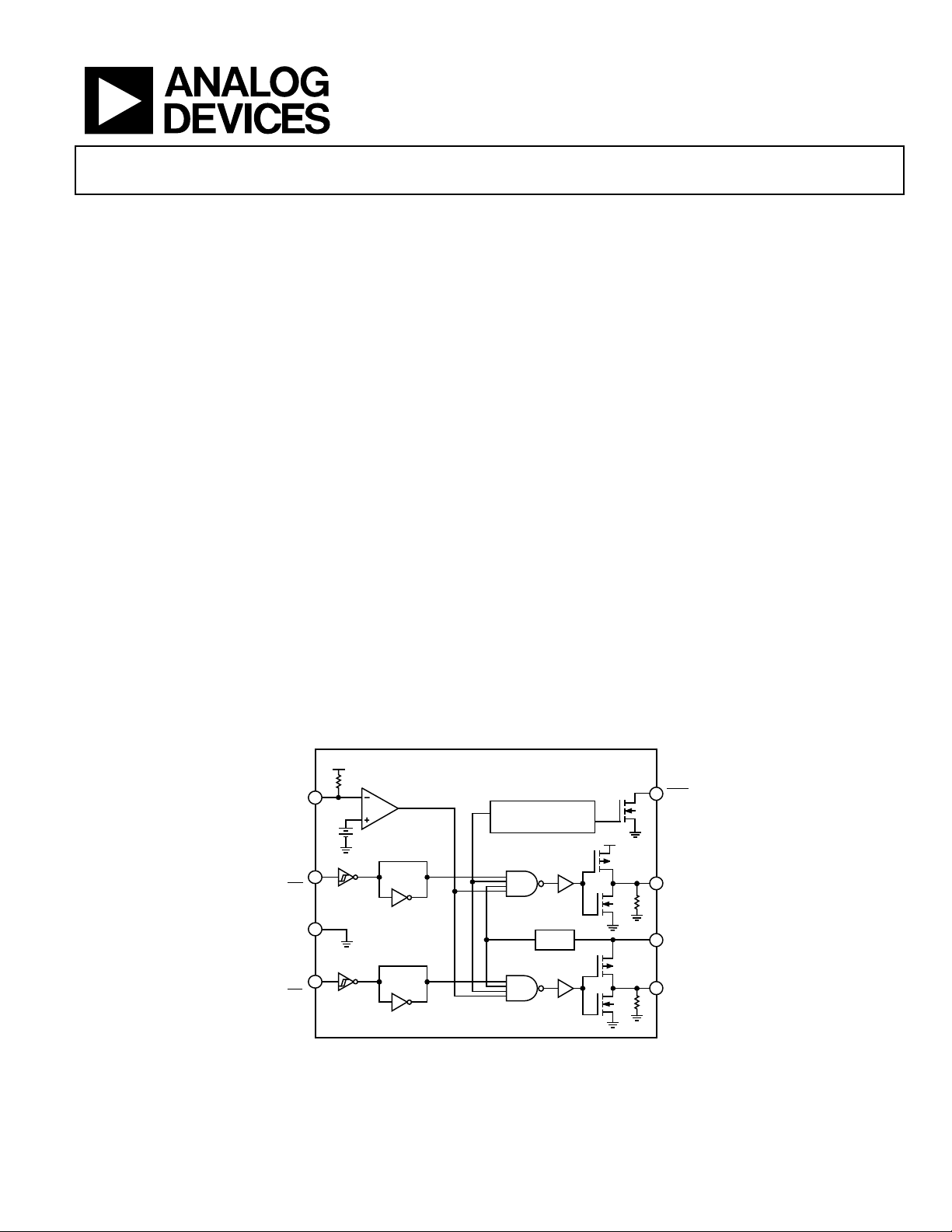
The ADP362x/ADP363x is a family of high current and dual high
speed drivers, capable of driving two independent N-channel
power MOSFETs. The family uses the industry-standard footprint but adds high speed switching performance and improved
system reliability.
The family has an internal temperature sensor and provides
two levels of overtemperature protection, an overtemperature
warning, and an overtemperature shutdown at extreme junction
temperatures.
The SD function, generated from a precise internal comparator,
provides fast system enable or shutdown. This feature allows
redundant overvoltage protection, complementing the protection inside the main controller device, or provides safe system
shutdown in the event of an overtemperature warning.
The wide input voltage range allows the driver to be compatible
with both analog and digital PWM controllers.
Digital power controllers are supplied from a low voltage
supply, and the driver is supplied from a higher voltage supply.
The ADP362x/ADP363x family adds UVLO and hysteresis
functions, allowing safe startup and shutdown of the higher
voltage supply when used with low voltage digital controllers.
The device family is available in thermally enhanced SOIC_N_EP
and MINI_SO_EP packaging to maximize high frequency and
current switching in a small printed circuit board (PCB) area.
FUNCTIONAL BLOCK DIAGRAM
Rev. A
Information furnished by Analog Devices is believed to be accurate and reliable. However, no
responsibility is assumed by Analog Devices for its use, nor for any infringements of patents or other
rights of third parties that may result from its use. Specifications subject to change without notice. No
license is granted by implication or otherwise under any patent or patent rights of Analog Devices.
Trademarks and registered trademarks are the property of their respective owners.
Figure 1.
One Technology Way, P.O. Box 9106, Norwood, MA 02062-9106, U.S.A.
Tel: 781.329.4700
Fax: 781.461.3113 ©2009 Analog Devices, Inc. All rights reserved.
www.analog.com
 Loading...