

320 mA Switched Capacitor
C
IN
1mF
CP2
2.2mF
CP1
2.2mF
V
IN
V
OUT
SD
V
OUT
V
IN
GND
ADP3610
C
O
1mF
a
FEATURES
Push-Pull Charge Pump Doubler Reduces Output Ripple
+3.0 V to +3.6 V Operation
> +5.4 V @ 320 mA Maximum Load
V
OUT
Output Impedance, R
Shutdown Capability
Overvoltage Protection: V
Operating Temperature Range: –208C to +858C
Thermally Enhanced 16-Lead TSSOP Package
APPLICATIONS
High Current Doublers
LCD Panels
Cellular Phones
Inductorless Boost Converters
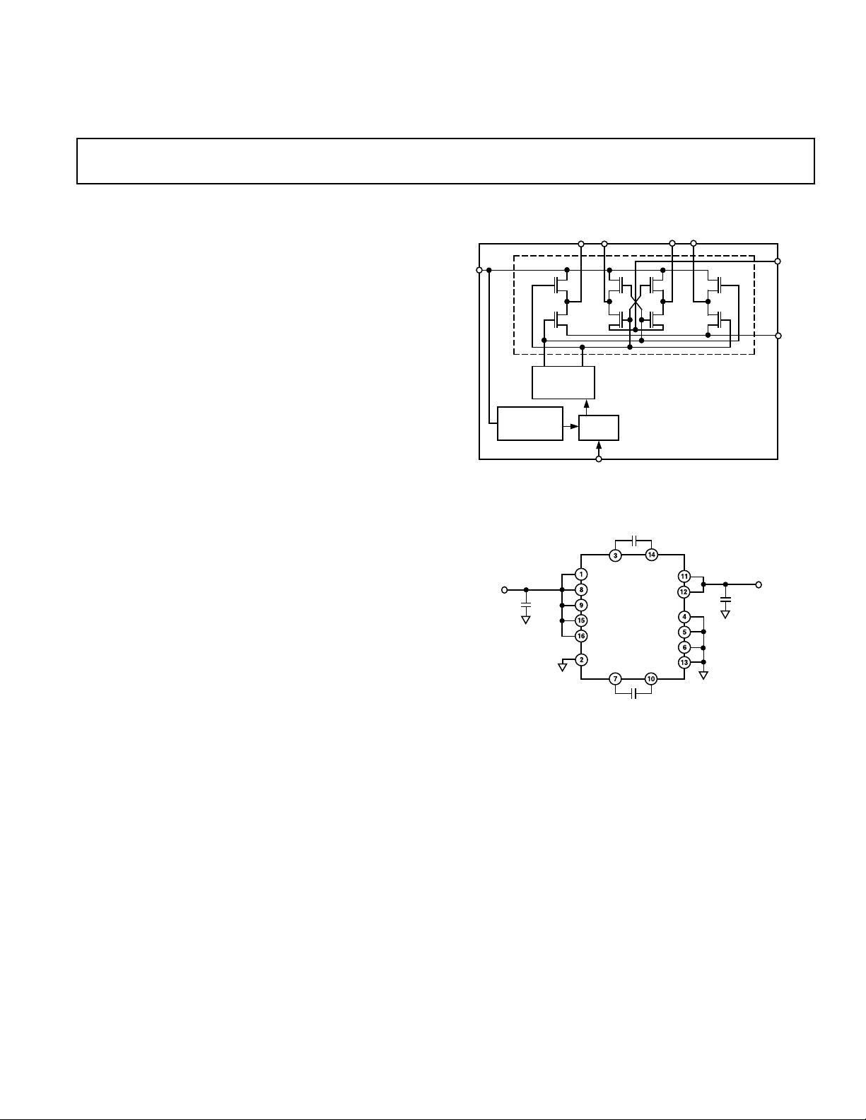
GENERAL DESCRIPTION
The ADP3610 is a push-pull switched-capacitor converter voltage doubler. The term “push-pull” refers to two charge pumps
working in parallel and in opposing phase to deliver charge to
support the output voltage. When one capacitor is pumping
charge to the output, the other is recharging. This technique
minimizes voltage loss and output voltage ripple.
The converter accommodates input voltages from +3 V to
+3.6 V and can provide 320 mA using 2.2 µF MLCC pump
capacitors. Converter operation can be enabled or disabled
simply by an input signal. The package is enhanced with Analog
Devices’ proprietary Thermal Coastline feature, which allows
up to 980 mW of power dissipation at room temperature. The
exceptionally thin TSSOP-16 package and the requirement of
only capacitors (no inductors) to support the converter operation allows slim designs, e.g., for TFT or LCD display panels.
TOTAL
≤ 1.66 V
> +4 V
IN
V
IN
Voltage Doubler
ADP3610
FUNCTIONAL BLOCK DIAGRAM
CM2CP2CM1CP1
DRV
DRV
DRIVE LOGIC
OVER-
VOLTAGE
PROTECTION
1MHz
OSC
SD
Figure 1. Typical Application Circuit
ADP3610
V
OUT
GND
REV. A
Information furnished by Analog Devices is believed to be accurate and
reliable. However, no responsibility is assumed by Analog Devices for its
use, nor for any infringements of patents or other rights of third parties
which may result from its use. No license is granted by implication or
otherwise under any patent or patent rights of Analog Devices.
One Technology Way, P.O. Box 9106, Norwood, MA 02062-9106, U.S.A.
Tel: 781/329-4700 World Wide Web Site: http://www.analog.com
Fax: 781/326-8703 © Analog Devices, Inc., 1999
ADP3610–SPECIFICATIONS
WARNING!
ESD SENSITIVE DEVICE
(–208C ≤ TA ≤ +858C, V
unless otherwise noted)
= +3.3 V, CP1 = CP2 = 2.2 mF, CO = 1 mF, SD = GND,
IN
1, 2, 3
Parameter Symbol Condition Min Typ Max Units
OPERATING SUPPLY RANGE V
QUIESCENT CURRENT I
IN
Q
SD = V
IN
3.0 3.6 V
0.3 µA
SD = GND, IL = 0 mA 8.6 10 mA
INPUT OVP THRESHOLD V
TOTAL OUTPUT IMPEDANCE R
OUTPUT VOLTAGE V
OVP
TOTAL
O
4
I
= 0 mA to 320 mA 1 1.66 Ω
O
IO = 240 mA, VIN = +3 V 5.6 5.75 V
I
= 320 mA, VIN = +3 V 5.47 5.65 V
O
I
= 240 mA, VIN = +3.3 V 6.2 6.35 V
O
4V
IO = 320 mA, VIN = +3.3 V 6.07 6.27 V
OUTPUT CURRENT I
OUTPUT SWITCHING FREQUENCY f
O
SW
320 mA
400 560 650 kHz
SD INPUT
Logic Input High V
Input Current I
Logic Input Low V
Input Current I
NOTES
1
Capacitors in the test circuit are multilayer ceramic type.
2
All limits at temperature extremes are guaranteed via correlation using standard Statistical Quality Control (SQC) methods.
3
Junction temperature is influenced by ambient temperature, device mounting and heatsinking, and power dissipation which is a function of I/O voltages and load.
4
R
includes the switch resistance, and the equivalent series resistance of the 2.2 µF (X7R) MLCC pump capacitors.
TOTAL
Specifications subject to change without notice.
IH
IH
IL
IL
2.0 V
0.1 µA
0.8 V
0.1 µA
ABSOLUTE MAXIMUM RATINGS
1
ORDERING GUIDE
Input Voltage (V+ to GND) . . . . . . . . . . . . . . . . . . . . +4.0 V
Output Short Circuit to GND (<1 A) . . . . . . . . . . . . . . 60 sec
Power Dissipation
2
θ
. . . . . . . . . . . . . . . . . . . . . . . . . . . . . . . . . . . .+102°C/W
JA
Operating Ambient Temperature Range . . . . –20°C to +85°C
Model Range Description Option
ADP3610ARU –20°C to +85°C Thin Shrink Small RU-16
Temperature Package Package
Storage Temperature Range . . . . . . . . . . . . –65°C to +150°C
Lead Temperature Range (Soldering 10 sec) . . . . . . . +300°C
Vapor Phase (60 sec) . . . . . . . . . . . . . . . . . . . . . . . +215°C
Infrared (15 sec) . . . . . . . . . . . . . . . . . . . . . . . . . . +220°C
NOTES
1
This is a stress rating only; operation beyond these limits can cause the device to
be permanently damaged.
2
θJA is specified for worst case conditions with device soldered on a FR-4, 1 oz.
copper clad four layer circuit board.
CAUTION
ESD (electrostatic discharge) sensitive device. Electrostatic charges as high as 4000 V readily
accumulate on the human body and test equipment and can discharge without detection.
Although the ADP3610 features proprietary ESD protection circuitry, permanent damage may
occur on devices subjected to high energy electrostatic discharges. Therefore, proper ESD
precautions are recommended to avoid performance degradation or loss of functionality.
Outline Package
(TSSOP-16)
–2–
REV. A
ADP3610
Table I. Other Members of ADP36xx Family
1
Output Package
Model Current Options2Comments
ADP3603 50 mA SO-8 Nom –3 V ± 3% Inverter
ADP3604 120 mA SO-8 Nom –3 V ± 3% Inverter
ADP3605-3 120 mA SO-8, Nom –3 V ± 5% Inverter
TSSOP-14
ADP3607-5 50 mA SO-8 Nom 5 V ± 5% Boost
ADP3607 50 mA SO-8 Adjustable ± 5% Boost
NOTES
1
See individual data sheets for detailed ordering information.
2
SO = Small Outline; TSSOP = Thin Shrink Small Outline Package.
Table II. Alternative Capacitor Technologies
Type Life High Freq Temp Size Cost
Aluminum
Electrolytic
Capacitor Fair Fair Fair Small Low
Multilayer
Ceramic
Capacitor Long Good Poor* Fair High
Solid
Tantalum Above
Capacitor Avg Avg Avg Avg Avg
OS-CON Above
Capacitor Avg Good Good Good Avg
*Refer to capacitor manufacturer’s data sheet for operation below 0°C.
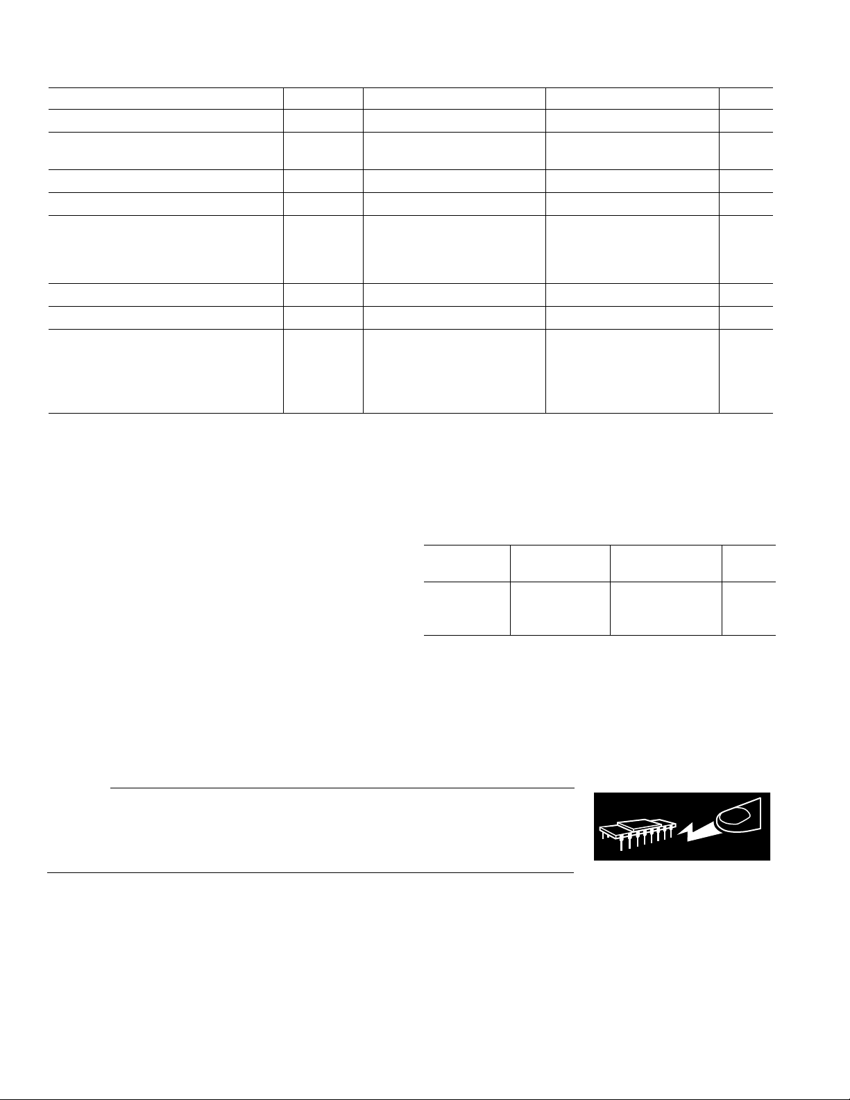
PIN FUNCTION DESCRIPTIONS
Pin Name Function
1, 8, 9, V
Input Voltage. Pins 1, 8, 9, 15 and 16
IN
15, 16 must be connected together for proper
operation.
2 SD Shutdown. A logic low input allows normal
operation. A logic high input shuts the device
off.
3 CM1 Pump Capacitor C1 Negative Input
4, 5, 6, GND Ground. Pins 4, 5, 6, and 13 must be
13 connected together for proper operation.
7 CM2 Pump Capacitor C2 Negative Input
10 CP2 Pump Capacitor C2 Positive Input
11, 12 V
Output Voltage. Pins 11 and 12 must be
OUT
connected together for proper operation.
14 CP1 Pump Capacitor C1 Positive Input
PIN CONFIGURATION
V
SD
CM1
GND
GND
GND
CM2
V
1
IN
2
3
4
5
6
7
8
IN
ADP3610
TOP VIEW
(Not to Scale)
V
16
IN
V
15
IN
CP1
14
GND
13
V
12
OUT
V
11
OUT
CP2
10
V
9
IN
Table III. Recommended Capacitor Manufacturers
Manufacturer Capacitor Capacitor Type
Sprague 672D, 673D, Aluminum Electrolytic
674D, 678D
Sprague 675D, 173D, Tantalum
199D
Nichicon PF and PL Aluminum Electrolytic
Mallory TDC and TDL Tantalum
TOKIN MLCC Multilayer Ceramic
MuRata GRM Multilayer Ceramic
REV. A
–3–

ADP3610
–Typical Performance Characteristics
570
IL = 0mA
565
560
555
OSCILLATOR FREQUENCY – kHz
550
2.7 3.62.8
2.9 3.0 3.1 3.2 3.3 3.4 3.5
SUPPLY VOLTAGE – Volts
Figure 2. Oscillator Frequency vs.
Supply Voltage
575
VIN = +3.0V
570
565
VIN = +3.3V
560
555
VIN = +3.6V
550
OSCILLATOR FREQUENCY – kHz
9.7
9.5
VIN = +3.6V
9.3
9.1
8.9
8.7
VIN = +3.3V
8.5
8.3
8.1
SUPPLY CURRENT – mA
VIN = +3.0V
7.9
7.7
–20 5 85
–10 35 50 65 80
20
TEMPERATURE – 8C
Figure 3. Supply Current vs.
Temperature
0.6
0.4
0.2
SUPPLY CURRENT – mA
VIN = +3.6V
VIN = +3.3V
VIN = +3.0V
6.62
6.59
6.56
6.53
6.50
6.47
6.44
6.41
6.38
6.35
6.32
OUTPUT VOLTAGE – Volts
6.29
6.26
6.23
–20 5 8520–10 35 50 65 80
VIN = +3.3V
I
= 0mA
L
VIN = +3.3V
I
= 320mA
L
TEMPERATURE – 8C
Figure 4. Output Voltage vs.
V
Temperature,
6.1
6.0
5.9
5.8
OUTPUT VOLTAGE – Volts
5.7
= +3.3 V
IN
545
–20 5 8520–10 35 50 65 80
TEMPERATURE – 8C
Figure 5. Oscillator Frequency vs.
Temperature
6.7
6.6
6.5
6.4
OUTPUT VOLTAGE – Volts
6.3
6.2
0 100 400
200 300
LOAD CURRENT – mA
Figure 8. Output Voltage vs. Load
Current for V
= +3.3 V
IN
0
–20 5 8520–10 35 50 65 80
TEMPERATURE – 8C
Figure 6. Supply Current in Shutdown
Mode vs. Temperature
7.3
7.2
7.1
7.0
OUTPUT VOLTAGE – Volts
6.9
6.8
0 100 400
200 300
LOAD CURRENT – mA
Figure 9. Output Voltage vs. Load
Current for V
= +3.6 V
IN
5.6
0 100 400
200 300
LOAD CURRENT – mA
Figure 7. Output Voltage vs. Load
Current for V
= +3.0 V␣
IN
–4–
REV. A

ADP3610
20
(mA)
Q
15
10
QUIESCENT CURRENT – I
IL = 0mA
5
3.0 3.2 3.4 3.6
IL = 320mA
– Volts
V
IN
Figure 10. Quiescent Current vs.
Input Voltage
100
80
60
40
EFFICIENCY – %
20
5
0 80 320160 240
LOAD CURRENT – mA
Figure 11. Efficiency vs. Load Current,
= +3.3 V
V
IN
10V
V
OUT
5V
0V
V
IN
V
SD
O
Figure 12. Output Voltage Ripple (IO =
µ
320 mA, CP1 = CP2 = 2.2
F, CO = 1 µF)
Figure 13. Start-Up Under Full Load
= +3.6 V, IO = 320 mA)
(V
IN
Figure 14. Shutdown at Full Load
= +3.3 V, IO = 320 mA)
(V
IN
REV. A
–5–
ADP3610
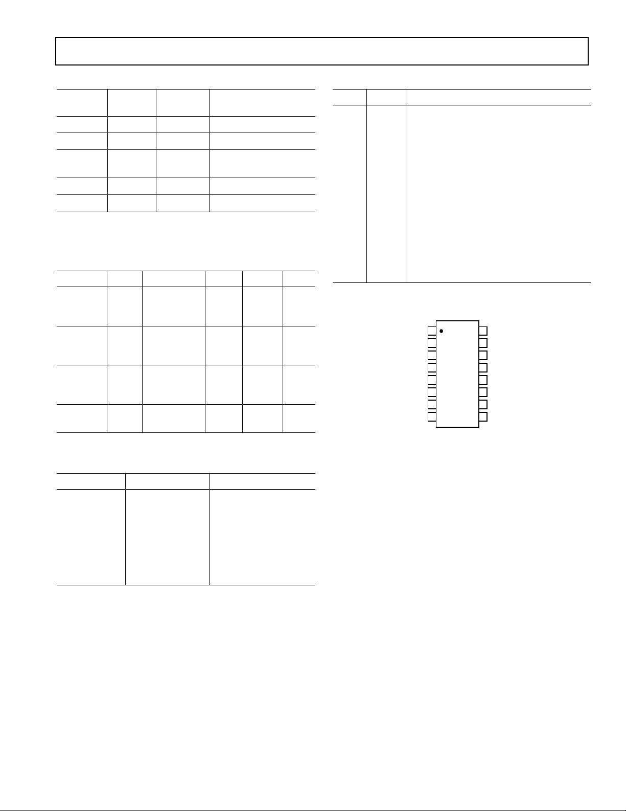
THEORY OF OPERATION
The ADP3610 is an unregulated switched capacitor voltage
doubler that provides an output voltage greater than 5.4 V from
a +3.0 V to +3.6 V input. The unique push-pull voltage doubling architecture allows it to deliver a maximum of 320 mA
output current. A typical application circuit, as shown in Figure
20, requires five small external capacitors. The ADP3610 has an
internal 1 MHz oscillator that is divided by two and used to
generate two nonoverlapping phase clocks.
The basic principle behind a conventional switched capacitor
voltage doubler is shown in Figure 15. During phase one, S1
and S2 are ON, charging the pump capacitor to the input voltage. In phase two, switches S1 and S2 are turned OFF and S3
and S4 are turned ON. During phase two, the pump capacitor
is placed in series with the input voltage, thereby charging the
output capacitor to the sum of input voltage and pump capacitor voltage, resulting in voltage doubling at the output
terminal.
f
S1
V
IN
S3
A
+
C
P
f
B
f
S4
S2
B
V
OUT
f
A
PHASE1PHASE
2
f
A
f
B
Figure 15. Conventional Voltage Doubler Configuration
The ADP3610 has two sets of switched capacitor voltage doublers connected in parallel delivering charge to the output as
shown in Figure 16.
PHASE 1
V
IN
PHASE 2
V
IN
f
S1
S4
S5
S8
S5
S8
A
f
B
f
B
f
A
f
S1
A
+
f
S4
B
f
B
+
f
A
+
+
S3
CP1
S2
S7
CP2
S6
S3
CP1
S2
S7
CP2
f
B
f
A
f
A
f
B
f
B
f
A
f
A
f
S6
B
V
OUT
(a)
V
OUT
(b)
Figure 17. (a) Phase 1 “Push” Charging␣
(b) Phase 2 “Pull” Charging
Overvoltage Protection
The input voltage is scaled with a resistor network and compared to the bandgap reference voltage of 1.25 V by a 50 mV
hysteresis comparator. When the input voltage exceeds 4.0 V,
the overvoltage protection signal stops the oscillator.
f
V
IN
S1
S4
S5
S8
f
f
f
A
CP1
B
B
CP2
A
+
+
f
S3
S2
S7
S6
B
f
A
f
A
f
B
V
OUT
Figure 16. Switch Configuration Charging the Pump
Capacitor
The two voltage doublers run in opposite phases, i.e., when one
pump capacitor is being charged, the other is charging the output, as shown in Figure 17. In this architecture, one of the
pump capacitors is always delivering charge to the output. As a
result, output ripple is at a frequency that is double the switching frequency. This allows the use of a smaller output capacitor
compared to a conventional voltage doubler.
V
IN
R1
R2
BANDGAP
= 1.25V
50mV
ADP3610
OSC
EN
Figure 18. Overvoltage Protection
Shutdown Mode
The ADP3610’s output can be disabled by pulling the SD pin
high to a TTL/CMOS logic compatible level which will stop the
internal oscillator. In shutdown mode, all analog circuitry including overvoltage protection is shut off, thereby reducing the
quiescent current to 10 µA typical. Applying a digital low level
or tying the SD pin to ground will turn on the output. If the
shutdown feature is not used, SD pin should be tied to the
ground pin. The output voltage in shutdown mode is approximately V
– 0.6 V.
IN
–6–
REV. A

ADP3610
APPLICATION INFORMATION
Capacitor Selection
The ADP3610’s high internal oscillator frequency permits the
use of small capacitors for both the pump and the output capacitors. For a given load current, factors affecting the output
voltage performance are:
• Pump (CP) and output (C
• ESR of the CP and C
O
O
) capacitance
When selecting the capacitors, keep in mind that not all manufacturers guarantee capacitor ESR in the range required by the
circuit. In general, the capacitor’s ESR is inversely proportional
to its physical size, so larger capacitance values and higher voltage ratings tend to reduce ESR. Since the ESR is also a function
of the operating frequency, when selecting a capacitor, make
sure its value is rated at the circuit’s operating frequency. Another factor affecting capacitor performance is temperature. Figure 19 illustrates the temperature effect on various capacitors.
Aluminium electrolytic capacitors lose their capacitance at
low temperatures and their ESR increases considerably. Some
capacitor technologies do offer improved performance over
temperature; for example, certain tantalum capacitors provide
good low temperature ESR but at a higher cost. Table II provides the ratings for different types of capacitor technologies to
help the designer select the right capacitors for the application.
The exact values of C
and CO are not critical. However, low
IN
ESR capacitors such as solid tantalum and multilayer ceramic
capacitors are recommended to minimize voltage loss at high
currents. Table III shows a partial list of the recommended low
ESR capacitor manufacturers.
Input Capacitor
A small 1 µF input bypass capacitor, preferably with low ESR,
such as tantalum or multilayer ceramic, is recommended to
reduce noise and supply transients and supply part of the peak
input current drawn by the ADP3610. A large capacitor is recommended if the input supply is connected to the ADP3610
through long leads, or if the pulse current drawn by the device
might affect other circuitry through supply coupling.
Output Capacitor
The output capacitor (CO) is alternately charged to the sum of
input voltage and pump capacitor voltage when CP is switched
in series with C
. The ESR of CO introduces steps in the V
O
OUT
waveform whenever the charge pump charges CO, which tends
to increase V
are recommended for C
ripple. Thus, ceramic or tantalum capacitors
OUT
to minimize ripple on the output.
O
Note that as the capacitor value increases beyond the point
where the dominant contribution to the output ripple is due to
the ESR, no significant reduction in V
ripple is achieved by
OUT
added capacitance.
Multiple smaller capacitors can be connected in parallel to yield
lower ESR and potential cost savings. For lighter loads, proportionally smaller capacitors are required. To reduce high fre-
quency noise, bypass the output with a 0.1 µF ceramic capacitor.
Pump Capacitor
The ADP3610 alternately charges CP to the input voltage when
it is switched in parallel with the input supply, and then transfers charge to C
when it is switched in series with the input and
O
connected to the output.
10
ALUMINUM
1.0
ESR – V
0.1
ORGANIC SEMIC
0.01
–50 0 10050
CERAMIC
TANTALUM
ORGANIC SEMIC
TANTALUM
CERAMIC
ALUMINUM
TEMPERATURE – 8C
Figure 19. ESR vs. Temperature
Power Dissipation
The power dissipation of the ADP3610 circuit must be limited
so the junction temperature of the device does not exceed the
maximum junction temperature rating. Total power dissipation
is calculated as follows:
P
= (2 VIN – V
D
Where I
and V
and IS are output current and supply current, V
OUT
are input and output voltages respectively.
OUT
For example: assuming worst case conditions, V
V
= 5.62 V, I
OUT
= 320 mA and IS = 14 mA. Calculated
OUT
OUT
) I
OUT
+ VIN (IS)
= 3 V,
IN
IN
device power dissipation is:
P
≈ (6 V – 5.62 V) × 0.32 + 3 × (0.014) = 163.6 mW
D
The proprietary thermal coastline package used in the ADP3610
has a thermal resistance of 102°C/W. Therefore, the rise in
junction temperature for this application would be:
T
= 0.164 W × 102°C/W = 16.7°C
RISE
General Board Layout Guidelines
Since the ADP3610’s internal switches turn on and off very fast,
good PC board layout practices are critical to ensure optimal
operation of the device. Improper layouts will result in poor load
regulation, especially under heavy loads. Following these simple
layout guidelines will improve output performance.
1. Use adequate ground and power traces or planes.
2. Use single point ground for device ground and input and
output capacitor grounds.
3. Keep external components as close to the device as possible.
4. Use short traces from the input and output capacitors to the
input and output pins respectively.
5. All multiple GND, V
and V
IN
pins must be connected
OUT
together for proper operation.
REV. A
–7–

ADP3610
Unregulated Voltage Doubler
Figure 20 shows a typical application for the ADP3610 in unregulated voltage doubling mode. The inherent limit on the
output voltage for a voltage doubler is two times the input voltage. However, due to the losses in the switches and ESR of
capacitors, this scaling factor is somewhat reduced. Figure 21
shows the magnitude of unregulated output voltage as the load
current is increased from 0 mA to 320 mA. This gives a measure
of the equivalent resistance R
TOTAL
. R
is comprised of
TOTAL
internal switch resistance and ESR of the capacitors.
CP1
2.2mF
C
V
= 3.3V
IN
INPUT
1mF
C
1mF
IN1
IN2
V
1
SD
2
CM1
3
GND
4
GND
5
GND
6
CM2
7
V
8
ADP3610
IN
CP1
GND
V
OUT
V
OUT
CP2
IN
V
16
IN
V
15
IN
14
13
12
11
10
V
9
IN
C
1mF
O
OUTPUT
= 6.2V
V
O
@320mA
6.0
4.5
3.0
OUTPUT VOLTAGE – Volts
1.5
0
0
100 200 300 400
Figure 21. Load Regulation
SLOPE = R
LOAD CURRENT – mA
V
IN
TOTAL
= 3 V
= = 1.18V
6 – 5.62
0.32
(5.62, 320 mA)
CP2
2.2mF
Figure 20. Unregulated Voltage Doubler
–8–
REV. A
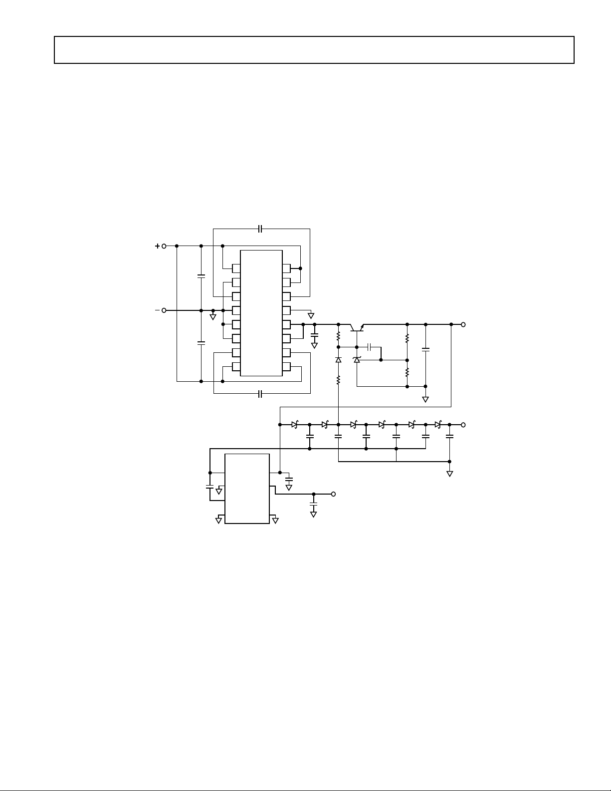
TFT LCD System Design
The ADP3610 is very useful for applications like notebook LCD
displays which require a low profile solution. Figure 22 shows a
typical LCD display application. A TFT LCD display requires
+5 V main voltage and +17 V and –5 V auxiliary voltages. The
ADP3610 doubles the input voltage, which is then fed through a
discrete linear regulator to generate +5 V. The main voltage is
also fed to the ADP3605, which inverts the input voltage to
generate –5 V. The CP+ node of the ADP3605 pump capacitor
is fed to a diode-capacitor ladder network to quadruple the main
voltage, i.e., 4 × V
– 6 × V
MAIN
= 3.0V TO 3.6V
V
IN
DIODE
1mF
1mF
≈ 17 V.
2.2mF
ADP3610
V
1
IN
SD
2
CM1
3
GND
4
GND
5
GND
6
CM2
7
V
8
IN
CP1
V
V
CP1
GND
V
OUT
V
OUT
CP2
V
16
IN
15
IN
14
13
12
11
10
9
IN
1mF
470V
1kV
0.1mF
TL431
25.5kV
24.9kV
1mF
V
MAIN
150mA
ADP3610
= 5V @
2.2mF
CP2
2.2mF
2.2mF 2.2mF 1mF 1mF 1mF 1mF
ADP3605
CP+
V
IN
V
GND
OUT
NC
CP–
V
SD
SNS
NC = NO CONNECT
1mF
2.2mF
VGL = –5V @
30mA
Figure 22. LCD Display Application
V
GH
3mA
= 17V @
REV. A
–9–

ADP3610
OUTLINE DIMENSIONS
Dimensions shown in inches and (mm).
16-Lead Thin Shrink Small Outline Package (TSSOP)
(RU-16)
0.201 (5.10)
0.193 (4.90)
16 9
0.177 (4.50)
0.006 (0.15)
0.002 (0.05)
SEATING
PLANE
0.169 (4.30)
1
PIN 1
0.0256
(0.65)
BSC
0.0118 (0.30)
0.0075 (0.19)
8
0.256 (6.50)
0.246 (6.25)
0.0433
(1.10)
MAX
0.0079 (0.20)
0.0035 (0.090)
8°
0°
0.028 (0.70)
0.020 (0.50)
C3442a–0–7/99
–10–
PRINTED IN U.S.A.
REV. A
 Loading...