320 mA Switched Capacitor
C
IN
1mF
CP2
2.2mF
CP1
2.2mF
V
IN
V
OUT
SD
V
OUT
V
IN
GND
ADP3610
C
O
1mF
a
FEATURES
Push-Pull Charge Pump Doubler Reduces Output Ripple
+3.0 V to +3.6 V Operation
> +5.4 V @ 320 mA Maximum Load
V
OUT
Output Impedance, R
Shutdown Capability
Overvoltage Protection: V
Operating Temperature Range: –208C to +858C
Thermally Enhanced 16-Lead TSSOP Package
APPLICATIONS
High Current Doublers
LCD Panels
Cellular Phones
Inductorless Boost Converters
GENERAL DESCRIPTION
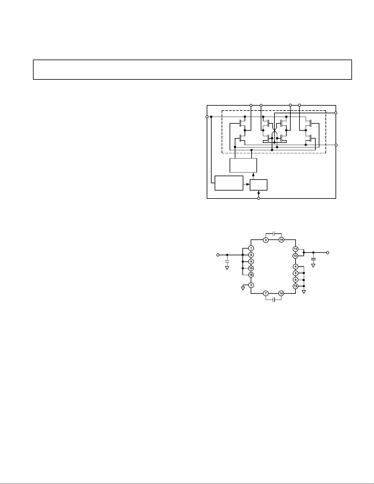
The ADP3610 is a push-pull switched-capacitor converter voltage doubler. The term “push-pull” refers to two charge pumps
working in parallel and in opposing phase to deliver charge to
support the output voltage. When one capacitor is pumping
charge to the output, the other is recharging. This technique
minimizes voltage loss and output voltage ripple.
The converter accommodates input voltages from +3 V to
+3.6 V and can provide 320 mA using 2.2 µF MLCC pump
capacitors. Converter operation can be enabled or disabled
simply by an input signal. The package is enhanced with Analog
Devices’ proprietary Thermal Coastline feature, which allows
up to 980 mW of power dissipation at room temperature. The
exceptionally thin TSSOP-16 package and the requirement of
only capacitors (no inductors) to support the converter operation allows slim designs, e.g., for TFT or LCD display panels.
TOTAL
≤ 1.66 V
> +4 V
IN
V
IN
Voltage Doubler
ADP3610
FUNCTIONAL BLOCK DIAGRAM
CM2CP2CM1CP1
DRV
DRV
DRIVE LOGIC
OVER-
VOLTAGE
PROTECTION
1MHz
OSC
SD
Figure 1. Typical Application Circuit
ADP3610
V
OUT
GND
REV. A
Information furnished by Analog Devices is believed to be accurate and
reliable. However, no responsibility is assumed by Analog Devices for its
use, nor for any infringements of patents or other rights of third parties
which may result from its use. No license is granted by implication or
otherwise under any patent or patent rights of Analog Devices.
One Technology Way, P.O. Box 9106, Norwood, MA 02062-9106, U.S.A.
Tel: 781/329-4700 World Wide Web Site: http://www.analog.com
Fax: 781/326-8703 © Analog Devices, Inc., 1999

ADP3610–SPECIFICATIONS
WARNING!
ESD SENSITIVE DEVICE
(–208C ≤ TA ≤ +858C, V
unless otherwise noted)
= +3.3 V, CP1 = CP2 = 2.2 mF, CO = 1 mF, SD = GND,
IN
1, 2, 3
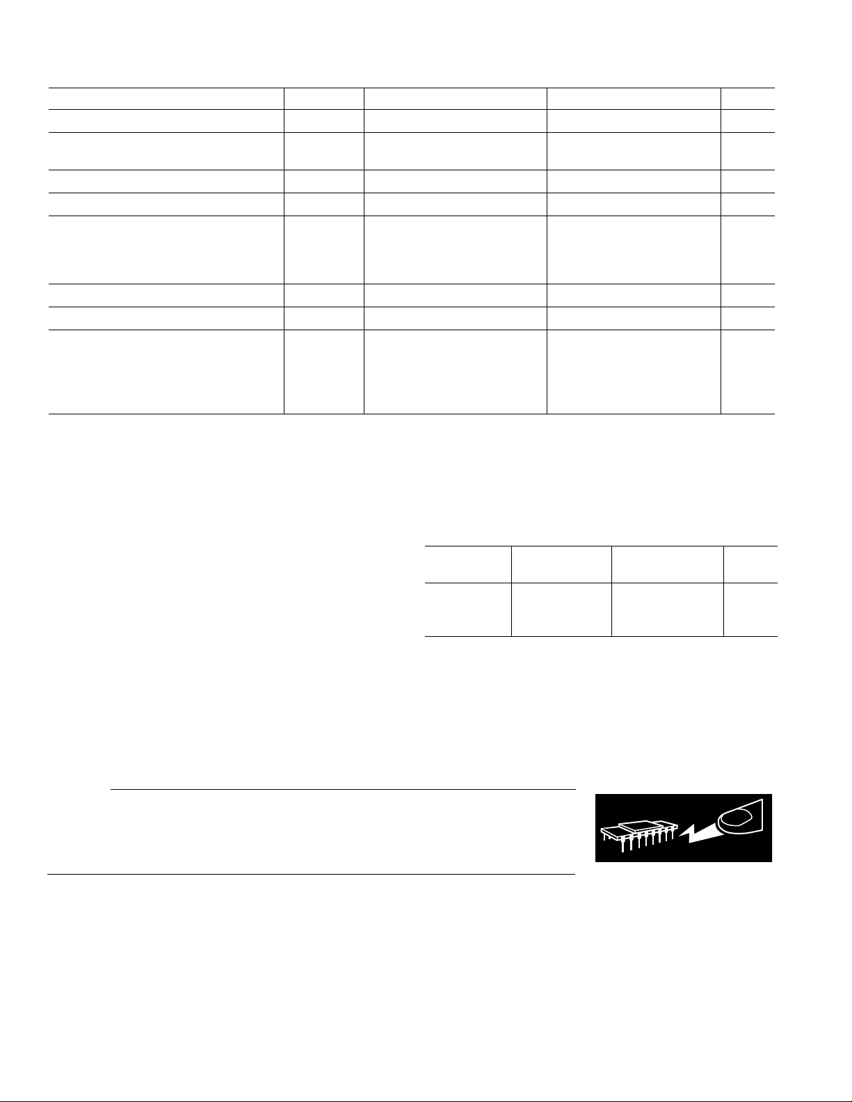
Parameter Symbol Condition Min Typ Max Units
OPERATING SUPPLY RANGE V
QUIESCENT CURRENT I
IN
Q
SD = V
IN
3.0 3.6 V
0.3 µA
SD = GND, IL = 0 mA 8.6 10 mA
INPUT OVP THRESHOLD V
TOTAL OUTPUT IMPEDANCE R
OUTPUT VOLTAGE V
OVP
TOTAL
O
4
I
= 0 mA to 320 mA 1 1.66 Ω
O
IO = 240 mA, VIN = +3 V 5.6 5.75 V
I
= 320 mA, VIN = +3 V 5.47 5.65 V
O
I
= 240 mA, VIN = +3.3 V 6.2 6.35 V
O
4V
IO = 320 mA, VIN = +3.3 V 6.07 6.27 V
OUTPUT CURRENT I
OUTPUT SWITCHING FREQUENCY f
O
SW
320 mA
400 560 650 kHz
SD INPUT
Logic Input High V
Input Current I
Logic Input Low V
Input Current I
NOTES
1
Capacitors in the test circuit are multilayer ceramic type.
2
All limits at temperature extremes are guaranteed via correlation using standard Statistical Quality Control (SQC) methods.
3
Junction temperature is influenced by ambient temperature, device mounting and heatsinking, and power dissipation which is a function of I/O voltages and load.
4
R
includes the switch resistance, and the equivalent series resistance of the 2.2 µF (X7R) MLCC pump capacitors.
TOTAL
Specifications subject to change without notice.
IH
IH
IL
IL
2.0 V
0.1 µA
0.8 V
0.1 µA
ABSOLUTE MAXIMUM RATINGS
1
ORDERING GUIDE
Input Voltage (V+ to GND) . . . . . . . . . . . . . . . . . . . . +4.0 V
Output Short Circuit to GND (<1 A) . . . . . . . . . . . . . . 60 sec
Power Dissipation
2
θ
. . . . . . . . . . . . . . . . . . . . . . . . . . . . . . . . . . . .+102°C/W
JA
Operating Ambient Temperature Range . . . . –20°C to +85°C
Model Range Description Option
ADP3610ARU –20°C to +85°C Thin Shrink Small RU-16
Temperature Package Package
Storage Temperature Range . . . . . . . . . . . . –65°C to +150°C
Lead Temperature Range (Soldering 10 sec) . . . . . . . +300°C
Vapor Phase (60 sec) . . . . . . . . . . . . . . . . . . . . . . . +215°C
Infrared (15 sec) . . . . . . . . . . . . . . . . . . . . . . . . . . +220°C
NOTES
1
This is a stress rating only; operation beyond these limits can cause the device to
be permanently damaged.
2
θJA is specified for worst case conditions with device soldered on a FR-4, 1 oz.
copper clad four layer circuit board.
CAUTION
ESD (electrostatic discharge) sensitive device. Electrostatic charges as high as 4000 V readily
accumulate on the human body and test equipment and can discharge without detection.
Although the ADP3610 features proprietary ESD protection circuitry, permanent damage may
occur on devices subjected to high energy electrostatic discharges. Therefore, proper ESD
precautions are recommended to avoid performance degradation or loss of functionality.
Outline Package
(TSSOP-16)
–2–
REV. A

ADP3610
Table I. Other Members of ADP36xx Family
1
Output Package
Model Current Options2Comments
ADP3603 50 mA SO-8 Nom –3 V ± 3% Inverter
ADP3604 120 mA SO-8 Nom –3 V ± 3% Inverter
ADP3605-3 120 mA SO-8, Nom –3 V ± 5% Inverter
TSSOP-14
ADP3607-5 50 mA SO-8 Nom 5 V ± 5% Boost
ADP3607 50 mA SO-8 Adjustable ± 5% Boost
NOTES
1
See individual data sheets for detailed ordering information.
2
SO = Small Outline; TSSOP = Thin Shrink Small Outline Package.
Table II. Alternative Capacitor Technologies
Type Life High Freq Temp Size Cost
Aluminum
Electrolytic
Capacitor Fair Fair Fair Small Low
Multilayer
Ceramic
Capacitor Long Good Poor* Fair High
Solid
Tantalum Above
Capacitor Avg Avg Avg Avg Avg
OS-CON Above
Capacitor Avg Good Good Good Avg
*Refer to capacitor manufacturer’s data sheet for operation below 0°C.
PIN FUNCTION DESCRIPTIONS
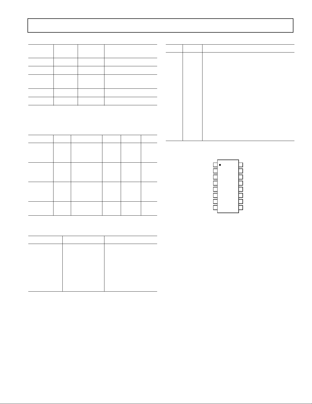
Pin Name Function
1, 8, 9, V
Input Voltage. Pins 1, 8, 9, 15 and 16
IN
15, 16 must be connected together for proper
operation.
2 SD Shutdown. A logic low input allows normal
operation. A logic high input shuts the device
off.
3 CM1 Pump Capacitor C1 Negative Input
4, 5, 6, GND Ground. Pins 4, 5, 6, and 13 must be
13 connected together for proper operation.
7 CM2 Pump Capacitor C2 Negative Input
10 CP2 Pump Capacitor C2 Positive Input
11, 12 V
Output Voltage. Pins 11 and 12 must be
OUT
connected together for proper operation.
14 CP1 Pump Capacitor C1 Positive Input
PIN CONFIGURATION
V
SD
CM1
GND
GND
GND
CM2
V
1
IN
2
3
4
5
6
7
8
IN
ADP3610
TOP VIEW
(Not to Scale)
V
16
IN
V
15
IN
CP1
14
GND
13
V
12
OUT
V
11
OUT
CP2
10
V
9
IN
Table III. Recommended Capacitor Manufacturers
Manufacturer Capacitor Capacitor Type
Sprague 672D, 673D, Aluminum Electrolytic
674D, 678D
Sprague 675D, 173D, Tantalum
199D
Nichicon PF and PL Aluminum Electrolytic
Mallory TDC and TDL Tantalum
TOKIN MLCC Multilayer Ceramic
MuRata GRM Multilayer Ceramic
REV. A
–3–
 Loading...