Analog Devices ADP3605ARU-3, ADP3605AR-3, ADP3605AR Datasheet

120 mA Switched Capacitor
SD
OSC
CLOCK
GEN
FEEDBACK
CONTROL
LOOP
SD
SD
B
SD
SDN
C
P
+
C
P
–
PN
N
S1
S3
V
IN
V
OUT
V
SENSE
GND
S2
S4
ADP3605
a
Voltage Inverter with Regulated Output
FEATURES
Fully Regulated Output Voltage (–3 V and Adjustable)
High Output Current: 120 mA
Output Accuracy: ⴞ3%
250 kHz Switching Frequency
Low Shutdown Current: 2 A Typical
Input Voltage Range from 3 V to 6 V
SO-8 and RU-14 Packages
–40ⴗC to +85ⴗC Ambient Temperature Range
APPLICATIONS
Voltage Inverters
Voltage Regulators
Computer Peripherals and Add-On Cards
Portable Instruments
Battery Powered Devices
Pagers and Radio Control Receivers
Disk Drives
Mobile Phones
ADP3605
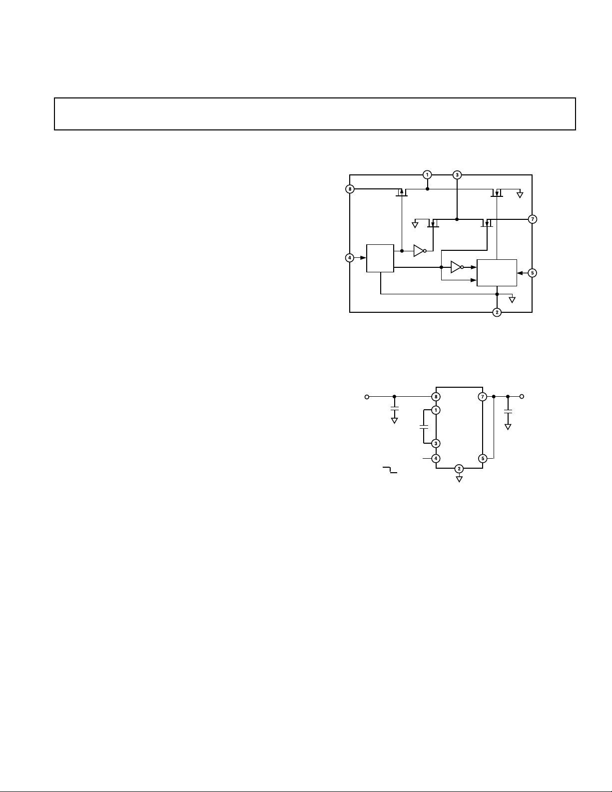
FUNCTIONAL BLOCK DIAGRAM
GENERAL DESCRIPTION
+
SENSE
*C
4.7mF
–3.0VV
O
The ADP3605 is a 120 mA regulated output switched capacitor
voltage inverter. It provides a regulated output voltage with
minimum voltage loss and requires a minimum number of external components. In addition, the ADP3605 does not require
the use of an inductor.
Pin-for-pin and functionally compatible with the ADP3604, the
internal oscillator of the ADP3605 runs at 500 kHz nominal
frequency which produces an output switching frequency of
250 kHz. This allows for the use of smaller charge pump and
filter capacitors.
The ADP3605 provides an accuracy of ±3% with a typical shutdown current of 2 µA. It can also operate from a single positive
V
V
+
IN
OUT
CP+
ADP3605-3
–
C
P
GND
IN
+
*C
IN
4.7mF
OFF
*FOR BEST PERFORMANCE, 10mF IS RECOMMENDED
C
P
C
IN
*C
P
4.7mF
SD
ON
0
: SPRAGUE, 293D475X0010B2W
, CO: TOKIN, 1E475ZY5UC205F
Figure 1. Typical Application Circuit
V
input voltage as low as 3 V. The ADP3605 is offered with the
regulation fixed at –3 V or adjustable via external resistors over
a –3 V to –6 V range.
REV. A
Information furnished by Analog Devices is believed to be accurate and
reliable. However, no responsibility is assumed by Analog Devices for its
use, nor for any infringements of patents or other rights of third parties
which may result from its use. No license is granted by implication or
otherwise under any patent or patent rights of Analog Devices.
One Technology Way, P.O. Box 9106, Norwood, MA 02062-9106, U.S.A.
Tel: 781/329-4700 World Wide Web Site: http://www.analog.com
Fax: 781/326-8703 © Analog Devices, Inc., 1999

1, 2, 3
ADP3605–SPECIFICATIONS
Parameter Symbol Conditions Min Typ Max Units
OPERATING SUPPLY RANGE V
SUPPLY CURRENT I
Shutdown Mode V
OUTPUT VOLTAGE
4
LOAD REGULATION ∆V
OUTPUT RESISTANCE
Open Loop R
OUTPUT RIPPLE VOLTAGE V
SWITCHING FREQUENCY F
SHUTDOWN
Logic Input High V
Input Current I
Logic Input Low V
Input Current I
NOTES
1
Capacitors C
2
See Figure 1 Conditions.
3
All limits at temperature extremes are guaranteed via correlation using standard Statistical Quality Control (SQC) methods.
4
For the adjustable device, a 1% resistor should be used to maintain output voltage tolerance. For both device types, tolerances can be improved by >1% using larger
value and lower ESR capacitors for CO and CP.
Specifications subject to change without notice.
IN, CO
and C
in the test circuit are 4.7 µF with 0.1 Ω ESR.
P
S
S
V
O
O
RIPPLE
S
IH
IH
IL
IL
O/IO
(VIN = 5.0 V @ TA = +25ⴗC, CP = CO = 4.7 F unless otherwise noted)
356V
–40°C < TA < +85°C36mA
SD
= V
IN
215µA
–40°C < TA < +85°C
IO = 60 mA –3.09 –3.0 –2.91 V
= 10 mA–120 mA, –3.15 –3 –2.85 V
I
O
–40°C ≤ T
≤ +85°C
A
4.75 V ≤ VS ≤ 6.0 V
IO = 10 mA–60 mA 0.3 mV/mA
IO = 10 mA–120 mA 0.25 mV/mA
9 Ω
C
= C
= 4.7 µF,
IN
I
I
O
= 60 mA 38 mV
LOAD
= 120 mA 75 mV
LOAD
VIN = 5 V 212 250 288 kHz
–40°C < TA < +85°C
2.4 V
1 µA
0.4 V
1 µA
ABSOLUTE MAXIMUM RATINGS
(T
= +25°C unless otherwise noted)
A
Input Voltage (V+ to GND, GND to OUT) . . . . . . . . +7.5 V
Input Voltage (V+ to OUT) . . . . . . . . . . . . . . . . . . . . . +11 V
Output Short Circuit Protection . . . . . . . . . . . . . . . . . . . 1 sec
Power Dissipation, SO-8 . . . . . . . . . . . . . . . . . . . . . . 660 mW
2
. . . . . . . . . . . . . . . . . . . . . . . . . . . . . . . . . . . . . . . . 150°C/W
θ
JA
Power Dissipation, RU-14 . . . . . . . . . . . . . . . . . . . . . 600 mW
2
. . . . . . . . . . . . . . . . . . . . . . . . . . . . . . . . . . . . . . . . 165°C/W
θ
JA
1
Storage Temperature Range . . . . . . . . . . . . –65°C to +150°C
Lead Temperature Range (Soldering 10 sec) . . . . . . . .+300°C
Vapor Phase (60 sec) . . . . . . . . . . . . . . . . . . . . . . . .+215°C
Infrared (15 sec) . . . . . . . . . . . . . . . . . . . . . . . . . . .+220°C
NOTES
1
This is a stress rating only; operation beyond these limits can cause the device to
be permanently damaged.
2
θ
is specified for worst case conditions with device soldered on a circuit board.
JA
Operating Temperature Range . . . . . . . . . . . –40°C to +85°C
ORDERING GUIDE
Model Output Voltage Package Description Package Options*
ADP3605AR-3 –3 V Small Outline SO-8
ADP3605AR ADJ Small Outline SO-8
ADP3605ARU-3 –3 V Thin Shrink Small Outline Package (TSSOP) RU-14
*Contact the factory for the availability of other output voltage options.
–2–
REV. A

ADP3605
WARNING!
ESD SENSITIVE DEVICE
ADP3605
NC
NC
NC
V
IN
V
OUT
NC
V
SENSE
NC
NC
NC
SD
CP–
GND
C
P
+
NC = NO CONNECT
Table I. Other Members of ADP36xx Family
1
Output Package
Model Current Option2Comments
ADP3603AR 50 mA SO-8 Nom.–3 ± 3% Inverter
ADP3604AR 120 mA SO-8 Nom.–3 ± 3% Inverter
ADP3610ARU 320 mA TSSOP-16 Nom. 3.3 VIN Doubler
NOTES
1
See individual data sheets for detailed ordering information.
2
SO = Small Outline; TSSOP = Thin Shrink Small Outline Package.
Table II. Alternative Capacitor Technologies
High
Type Life Freq Temp Size Cost
Aluminum
Electrolytic
Capacitor Fair Fair Fair Small Low
Multilayer
Ceramic
Capacitor Long Good Poor Fair1High
Solid
Tantalum Above
Capacitor Avg Avg Avg Avg Avg
OS-CON Above
Capacitor Avg Good Good Good Avg
NOTE
1
Refer to capacitor manufacturer's data sheet for operation below 0°C.
Table III. Recommended Capacitor Manufacturers
Manufacturer Capacitor Capacitor Type
Sprague 672D, 673D,
674D, 678D Aluminum Electrolytic
Sprague 675D, 173D,
199D Tantalum
Nichicon PF and PL Aluminum Electrolytic
Mallory TDC and TDL Tantalum
TOKIN MLCC Multilayer Ceramic
MuRata GRM Multilayer Ceramic
PIN FUNCTION DESCRIPTIONS
Pin Pin
SO-8 TSSOP Name Function
14 C
+ Positive Terminal for the Pump
P
Capacitor.
2 5 GND Device Ground.
36 C
– Negative Terminal for the Pump
P
Capacitor.
4 7 SD Logic Level Shutdown Pin. Apply a
logic high or connect to V
to shut-
IN
down the device. In shutdown mode,
the charge pump is turned off and
quiescent current is reduced to 2 µA
(typical). Apply a logic low or con-
nect to ground for normal operation.
58 V
SENSE
Output Voltage Sense Line. This is
used to improve load regulation by
eliminating IR drop on the high
current carrying output traces. For
normal operation, connect V
V
. See Application section for
OUT
SENSE
to
more detail.
6 1, 2, 3,
9, 12,
13, 14 NC No Connection.
710 V
OUT
Regulated Negative Output Voltage.
Connect a low ESR, 4.7 µF or larger
capacitor between this pin and de-
vice GND.
811 V
IN
Positive Supply Input Voltage. Con-
nect a low ESR bypass capacitor
between this pin and device ground
to minimize supply transients.
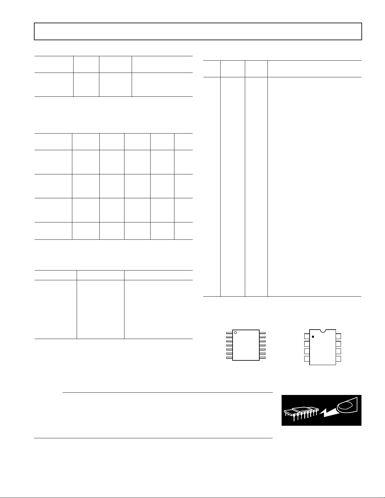
PIN CONFIGURATIONS
RU-14 SO-8
1
+
C
P
2
ADP3605
GND
TOP VIEW
3
C
–
P
(Not to Scale)
4
SD
NC = NO CONNECT
8
V
IN
7
V
OUT
6
NC
5
V
SENSE
CAUTION
ESD (electrostatic discharge) sensitive device. Electrostatic charges as high as 4000 V readily
accumulate on the human body and test equipment and can discharge without detection.
Although the ADP3605 features proprietary ESD protection circuitry, permanent damage may
occur on devices subjected to high energy electrostatic discharges larger than 600 V HBM.
Therefore, proper ESD precautions are recommended to avoid performance degradation or loss
of functionality.
–3–REV. A
 Loading...