Analog Devices ADP3603 Datasheet

REV. 0
Information furnished by Analog Devices is believed to be accurate and
reliable. However, no responsibility is assumed by Analog Devices for its
use, nor for any infringements of patents or other rights of third parties
which may result from its use. No license is granted by implication or
otherwise under any patent or patent rights of Analog Devices.
a
Switched Capacitor Voltage Converter
with Regulated Output
ADP3603*
© Analog Devices, Inc., 1996
One Technology Way, P.O. Box 9106, Norwood, MA 02062-9106, U.S.A.
Tel: 617/329-4700 Fax: 617/326-8703
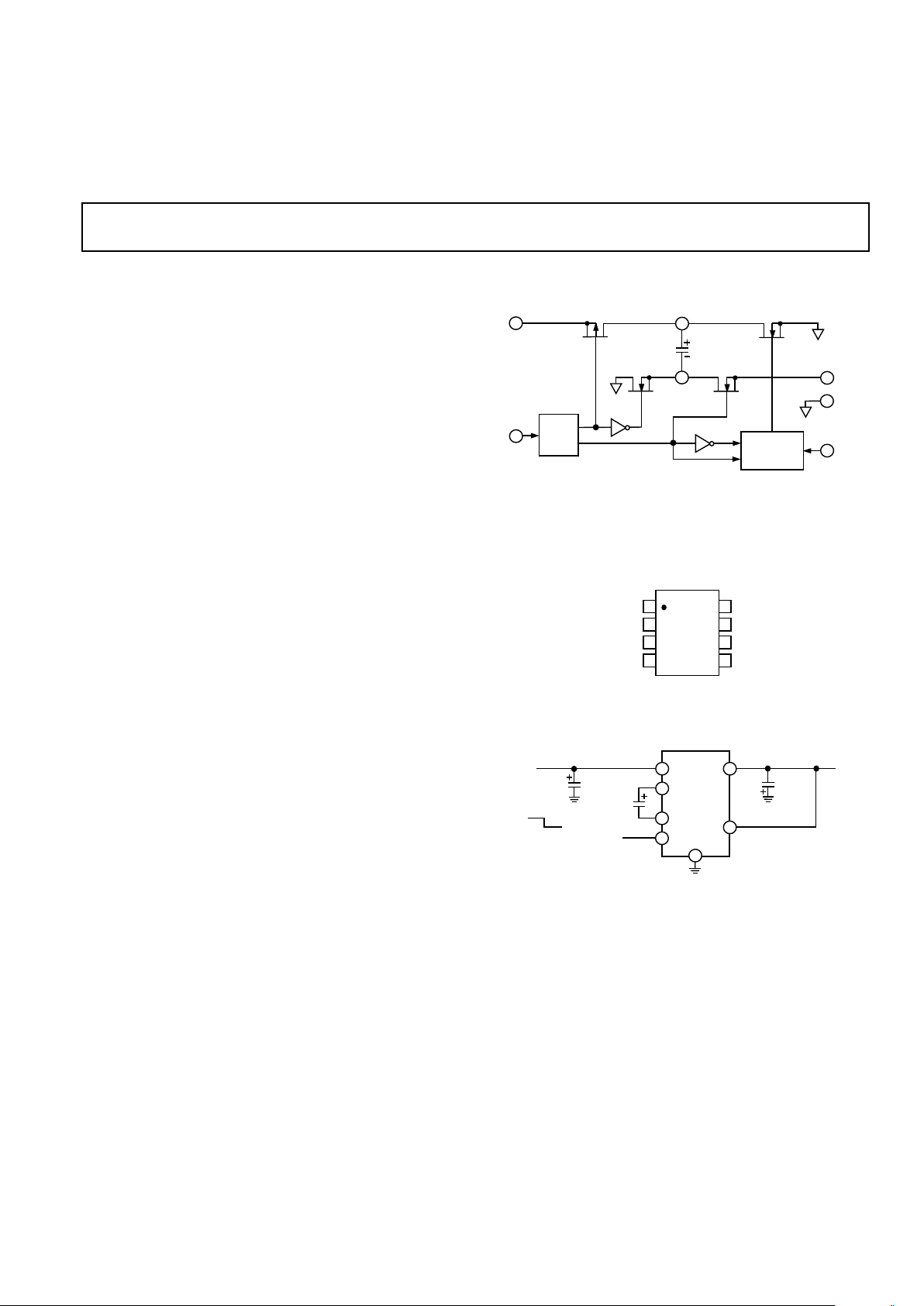
FUNCTIONAL BLOCK DIAGRAM
8
SPD
S1
SND
S2
S
N
D
B
S3
S
ND
7
3
V
IN
CP–
CP+
1
S4
2
V
OUT
GND
OSC
CLOCK
GEN
4
SD
FEEDBACK
CONTROL
LOOP
5
V
SENSE
GENERAL DESCRIPTION
The ADP3603 switched capacitor voltage converter provides
a regulated output voltage with minimum voltage loss and requires a minimum number of external components. In addition,
the ADP3603 does not require the use of an inductor. The
ADP3603 provides up to 50 mA of output current with ± 3%
output accuracy.
The internal oscillator runs at 240 kHz nominal frequency
which produces an output switching frequency of 120 kHz,
allowing the use of small charge pump and filter capacitors.
The ADP3603 is primarily designed for use as a high frequency negative voltage regulator/inverter. The output voltages
of the ADP3603 can range from –1.2 V to –4.0 V, nominally
–3.0 V. For other output voltages, contact the factory.
The ADP3603 dissipates less than 150 mW of power and features fast shutdown mode capability (<5 ms) that also drops the
quiescent current to 1.4 mA (typ). For a higher output current
(120 mA) version, see the ADP3604.
*Patent pending.
FEATURES
Fully Regulated Output
High Output Current: 50 mA
120 mA Version (ADP3604) Is Also Available
Outstanding Precision: 63% Output Accuracy
Input Voltage Range: +4.5 V to +6.0 V
Output Voltage: –3.0 V (Regulated)
High Switching Frequency: 120 kHz (240 kHz Internal
Oscillator)
Shutdown Capability
Small Outline 8-Pin SOIC Package
APPLICATIONS
Voltage Inverters
Negative Voltage Regulators
Computer Peripherals and Add-On Cards
Portable Instruments
Battery Powered Devices
Pagers and Radio Control Receivers
Disk Drives
Mobile Phones
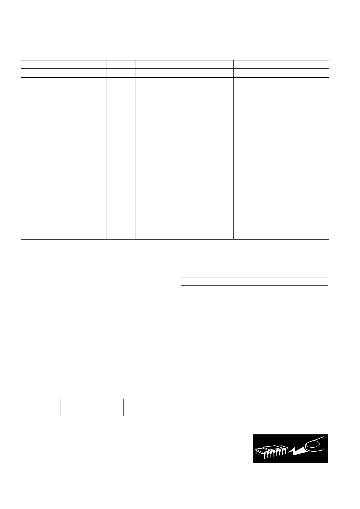
PIN CONFIGURATION
8-Pin SOIC
(SO-8)
1
2
3
4
8
7
6
5
TOP VIEW
(Not to Scale)
NC = NO CONNECT
ADP3603
CP+
V
SENSE
NC
V
OUT
V
IN
GND
CP–
SHUTDOWN
ADP3603
8
7
3
C2
4.7µF
†
1
4
SHUTDOWN
0
OFF
ON
C1
4.7µF
†
VIN +4.5 – +6V V
OUT
–3.0V
C3
4.7µF
†
2
5
V
SENSE
NOTE
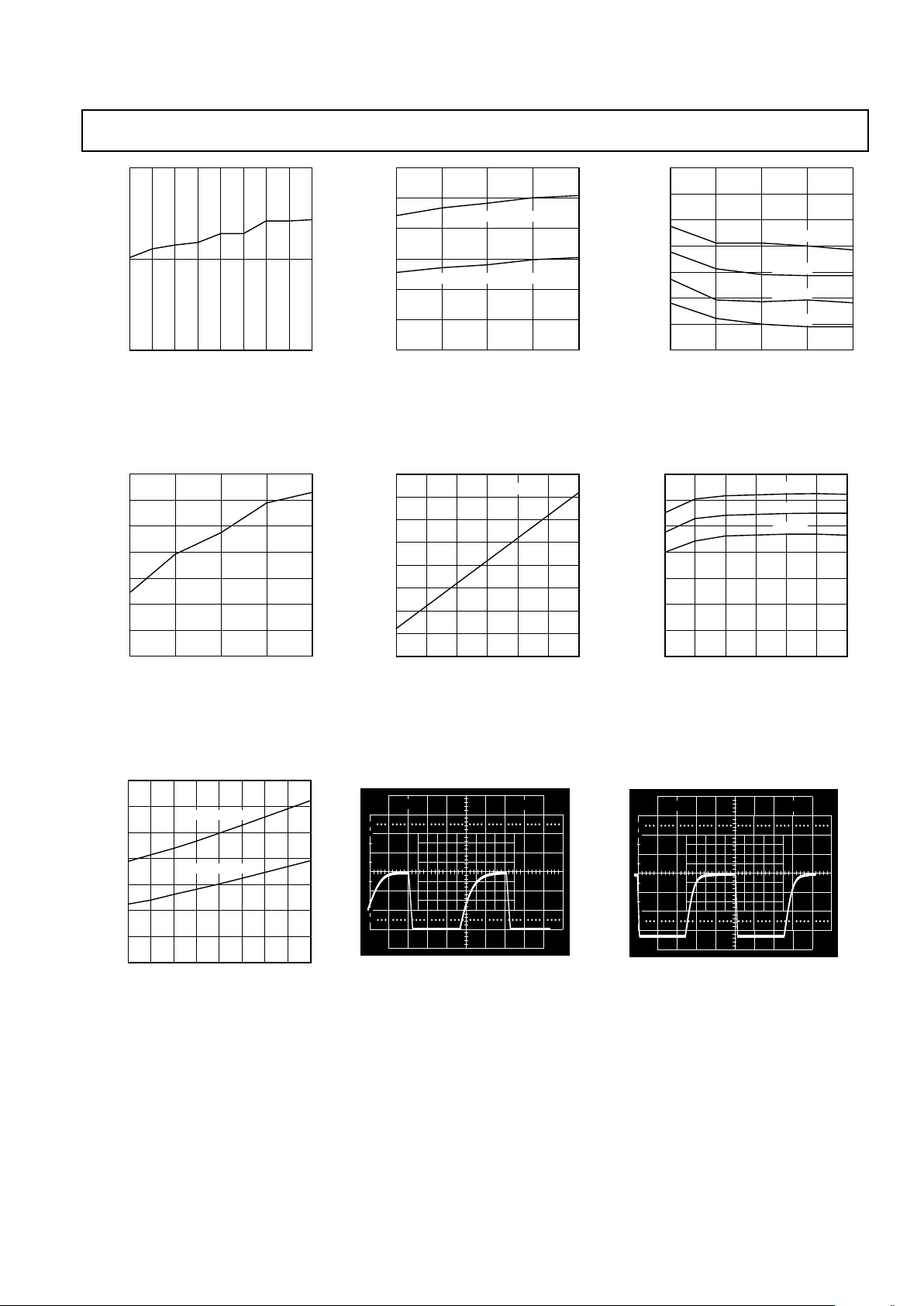
C2: SPRAGUE, 293D105X0010B2W
C1, C3: TOKIN, 1E105ZY5UC205F
†
FOR BEST PERFORMANCE 10µF IS RECOMMENDED
Figure 1. Typical Application Circuit

PIN DESCRIPTION
Pin Function
1C
P
+, Pump Capacitor Positive Input.
2 Ground.
3C
P
–, Pump Capacitor Negative Input.
4 Shutdown, Logic Level Shutdown Pin. Application of a
logic low to this pin will place the regulator in normal
operation. The device will be put into shutdown mode
with the shutdown pin pulled to V
IN
. In Shutdown
mode the charge pump is turned off. Connect to ground
for normal operation.
5V
SENSE
, Output Voltage Sense Line. This is used to improve load regulation performance by eliminating IR
drop on the output traces. See application section for
more detail. For normal operation, connect Pin 5 to
V
OUT
(Pin 7).
6 NC, No Internal Electrical Connection.
7V
OUT,
Output Pin. Regulated negative output voltage.
Connect a low ESR capacitor between this pin and device GND.
8V
IN,
Positive Supply Input when 4.5 V ≤ V
IN
≤ 6 V. Connect a low-ESR bypass capacitor between this pin and
the device ground pin.
Parameter Symbol Condition Min Typ Max Units
OPERATING SUPPLY RANGE V
S
4.5 5 6 V
SUPPLY CURRENT I
S
2.4 3 mA
–40°C < T
A
< +85°C 2.5 3.5 mA
Shutdown Mode 1.4 2 mA
–40°C < TA < +85°C 1.5 2.5 mA
OUTPUT
Output Voltage V
O
IO = 25 mA –3.1 –3 –2.91 V
V
O
IO = 10 mA to 50 mA, 4.5 V < VIN < 6 V –3.1 –3 –2.9 V
V
O
IO = 10 mA to 50 mA, 4.5 V < VIN < 6 V,
0°C < T
A
< +70°C –3.12 –3 –2.88 V
V
O
IO = 10 mA to 50 mA, 4.5 V < VIN < 6 V,
–40°C < T
A
< +85°C –3.15 –3 –2.85 V
Load Regulation ∆V
O
/ I
O
IO = 10 mA–60 mA 0.9 mV/mA
I
O
= 10 mA–120 mA 1.5 mV/mA
Output Resistance
2
R
O
8 Ω
Output Ripple Voltage
3
V
RIPPLE
C1–C3 = 10 µF, I
LOAD
= 80 mA 25 mV
C1–C3 = 10 µF, I
LOAD
= 120 mA 55 mV
SWITCHING FREQUENCY F
S
100 120 130 kHz
–40°C < TA < +85°C 96 120 140 kHz
SHUTDOWN
Logic Input High V
IH
2.4 V
Input Current I
IH
1 µA
Logic Input Low V
IL
0.4 V
Input Current I
IL
1 µA
Turn-On-Time t
ON
Figure 1, IL = 120 mA 5 ms
Turn-Off-Time t
OFF
Figure 1, IL = 120 mA 5 ms
NOTES
1
Capacitors C1 and C2 used in the test circuit are 10 µF with 0.1 Ω ESR. Capacitors with higher ESR may reduce output voltage and efficiency.
2
Open-loop output resistance.
3
See Figure 1 conditions.
All limits at temperature extremes are guaranteed via correlation using standard Statistical Quality Control (SQC) methods.
Specifications subject to change without notice
.
REV. 0
–2–
ADP3603–SPECIFICA TIONS
WARNING!
ESD SENSITIVE DEVICE
CAUTION
ESD (electrostatic discharge) sensitive device. Electrostatic charges as high as 4000 V readily
accumulate on the human body and test equipment and can discharge without detection.
Although the ADP3603 features proprietary ESD protection circuitry, permanent damage may
occur on devices subjected to high energy electrostatic discharges. Therefore, proper ESD
precautions are recommended to avoid performance degradation or loss of functionality.
(VIN = 5.0 V @ TA = +258C, CP = C
OUT
= 10 mF unless otherwise noted)
ABSOLUTE MAXIMUM RATINGS
1
(TA = +25°C unless otherwise noted)
Input Voltage (V+ to GND, GND to OUT) . . . . . . . . . +7.5 V
Output Short Circuit Protection . . . . . . . . . . . . . . . . . . . .1 sec
Power Dissipation, SO-8 . . . . . . . . . . . . . . . . . . . . . . .660 mW
θ
JA
2
. . . . . . . . . . . . . . . . . . . . . . . . . . . . . . . . . . . . . 150°C/W
θ
JC
. . . . . . . . . . . . . . . . . . . . . . . . . . . . . . . . . . . . . . 41°C/W
Operating Temperature Range . . . . . . . . . . . . .–40°C to +85°C
Storage Temperature Range . . . . . . . . . . . . .–65°C to +150°C
Lead Temperature Range (Soldering 10 sec) . . . . . . . . +300°C
Vapor Phase (60 sec) . . . . . . . . . . . . . . . . . . . . . . . . +215°C
Infrared (15 sec) . . . . . . . . . . . . . . . . . . . . . . . . . . . . +220°C
NOTES
1
This is a stress rating only and functional operation of the device at these or any
other conditions above those indicated in the operation section of this specification
is not implied. Exposure to absolute maximum rating conditions for extended
periods may affect device reliability.
2
θJA is specified for worst case conditions with device soldered on a circuit board.
ORDERING GUIDE
Model Temperature Range Package Option*
ADP3603AR –40°C to +85°C SO-8
*SO = Small Outline Package.

ADP3603
REV. 0
–3–
SUPPLY VOLTAGE – Volts
OSCILLATOR FREQUENCY – kHz
130
4.0 4.5 8.0
5.0 5.5 6.5 7.0 7.56.0
120
110
Figure 2. Oscillator Frequency vs.
Supply Voltage
TEMPERATURE – 8C
OSCILLATOR FREQUENCY – kHz
126
112
–40 85
07025
124
122
120
118
116
114
Figure 5. Oscillator Frequency vs.
Temperature
SUPPLY VOLTAGE – Volts
SUPPLY CURRENT – mA
3.5
0
4.0 4.5 8.0
5.0 5.5 6.5 7.0 7.56.0
3.0
2.5
2.0
1.5
1.0
0.5
NORMAL MODE
SHUTDOWN MODE
Figure 8. Supply Current vs. Supply
Voltage
TEMPERATURE – 8C
SUPPLY CURRENT – mA
3.0
1.5
0
–40 85
07025
2.5
2.0
1.0
0.5
NORMAL MODE @ VIN = 5V
SHUTDOWN MODE @ VIN = 5V
Figure 3. Supply Current vs.
Temperature
LOAD CURRENT – mA
INPUT CURRENT – mA
80
40
0
10 20 70
30 50 6040
70
60
50
30
20
10
VIN = 5V
Figure 6. Average Input Current vs.
Load Current
100
90
10
0%
5ms
1V
0V
–3V
Figure 9. Start-Up Under Full Load
TEMPERATURE – 8C
OUTPUT VOLTAGE – Volts
–2.95
–3.02
–40 85
07025
–2.96
–2.97
–2.98
–2.99
–3.00
–3.01
IL = 75mA
IL = 50mA
IL = 25mA
IL = 10mA
Figure 4. Output Voltage vs.
Temperature
LOAD CURRENT – mA
EFFICIENCY – %
70
0
10 20 70
30 40 50 60
60
50
40
30
20
10
VIN = 4.5V
VIN = 5V
VIN = 6V
Figure 7. Efficiency vs. Load
Current and Input Voltage
100
90
10
0%
5ms
1V
0V
–3V
Figure 10. Enable/Disable Time
Under Full Load
 Loading...