

Analog Devices ADP3502 Datasheet
a
CDMA Power Management System
ADP3502
FEATURES
11 LDOs Optimized for Specific CDMA Subsystems
4 Backup LDOs for Standby Mode Operation
Ultra Low Standby Supply Current
High Accuracy Battery Charger (0.7%)
3 Li-Ion Battery Charge Modes
5 mA Precharge
Low Current Charge
Full Current Charge
Integrated RTC
Ambient Temperature: –30ⴗC to +85ⴗC
64-Lead 7 mm ⴛ 7 mm ⴛ 1 mm TQFP Package
APPLICATIONS
CDMA/CDMA2000/PCS Handsets
GENERAL DESCRIPTION
The ADP3502 is a multifunction chip optimized for CDMA-1x
cell phone power management. It offers a total power solution
for the handset baseband and RF section, including LDOs to
power 11 subsystems. Also integrated are a real-time clock
(RTC), serial bus interface, and charging control for Li-Ion/
Li-Polymer batteries. Sophisticated controls are available for
power-up during battery charging, keypad interface, GPIO/INT
function, and RTC function.
The ADP3502 is optimized for CDMA handsets powered by
single-cell Li-Ion batteries. Its high level of integration significantly reduces the design effort, number of discrete
components, and solution size/cost. The main-sub LDO
structure reduces the standby current consumption, and as a
result, greatly extends the standby time of the phone. System
operation has been proven to be fully compatible with
MSM51xx-based designs.
The ADP3502 comes in a 64-lead 7 mm × 7 mm × 1 mm
TQFP package and is specified over a wide temperature range of
–30°C to +85°C.
FUNCTIONAL BLOCK DIAGRAM
POWER ON
KEYPAD I/F
GPIO
SERIAL I/F
32kHz OUTPUT
CONTROL
RESET
OUTPUT
LOGIC
BLOCK
DELAY 10ms
INTERRUPT
CONTROL
LDO
CONTROL
RESET
RTC
COUNTER
STAY-ALIVE
TIMER
ANALOG
BLOCK
BATTERY
CHARGER
REFERENCE
LDO1 TO LDO11
VOLTA G E
DETECTOR
ADP3502
REV. 0
Information furnished by Analog Devices is believed to be accurate and
reliable. However, no responsibility is assumed by Analog Devices for its
use, nor for any infringements of patents or other rights of third parties that
may result from its use. No license is granted by implication or otherwise
under any patent or patent rights of Analog Devices. Trademarks and
registered trademarks are the property of their respective companies.
One Technology Way, P.O. Box 9106, Norwood, MA 02062-9106, U.S.A.
Tel: 781/329-4700 www.analog.com
Fax: 781/326-8703 © 2003 Analog Devices, Inc. All rights reserved.

ADP3502–SPECIFICATIONS
MAIN FUNCTIONS
(TA = –30ⴗC to +85ⴗC, C
= 1 F MLCC, VBAT = 3.6 V, unless otherwise noted. See Table II for C
VBAT
OUT
.)
Parameter Symbol Conditions Min Typ Max Unit
SHUTDOWN GND CURRENT IGND
Power OFF TA = –20°C to +60°C2545µA
LDO3b: ON, Connect to RTCV
through Schottky Diode
RTC/32K OSC: Active
All Other LDOs: OFF
All Logic Inputs: VBAT or GND
MVBAT: OFF
OPERATING GND CURRENT IGND
Standby Mode Operation (Light Load) LDO1b, LDO2b, LDO3b, 60 125 µA
LDO6b: ON
= 1 mA for LDO3b and LDO6b
I
O
= 3 mA for LDO1b
I
O
I
= 300 µA for LDO2b
O
All Other LDOs: OFF
RTC/32K OSC: Active
MVBAT: OFF
All Logic Output: No Load
Standby Mode Operation (Midload) LDO1, LDO2, LDO3, LDO6, 300 µA
All Sub-LDOs: ON, I
= 70% Load
O
All Other LDOs: OFF
RTC/32K OSC: Active
MVBAT: ON
All Logic Outputs: No Load
Active Operation LDO5: OFF 700 µA
All Other LDOs: ON, 70% Load
RTC/32K OSC: Active
All Logic Outputs: No Load
MVBAT: ON
THERMAL SHUTDOWN THRESHOLD 160 °C
THERMAL SHUTDOWN HYSTERESIS 35 °C
ADAPTER/ADPSUPPLY VOLTAGE RANGE VADP 5 12 V
VBAT VOLTAGE RANGE VBAT 3.3 5.5 V
LDO SPECIFICATIONS
(TA = 25ⴗC, C
= 1 F MLCC, VBAT = V
VBAT
+ 1 V, NRCAP = 0.1 F. See Table II for C
OUT
OUT
.)
Parameter Symbol Conditions Min Typ Max Unit
BASEBAND VDD MAIN-LDO (LDO1a)
Output Voltage V
Output Capacitor Required for Stability C
Dropout Voltage V
LDO1aIO
LDO1a
DO
= 1 mA to 150 mA 2.81 2.90 2.99 V
= –30°C to +85°C
T
A
2.2 µF
IO = 150 mA 200 mV
Start-Up Time from Shutdown 250 µs
BASEBAND VDD SUB-LDO (LDO1b)
Output Voltage V
LDO1bIO
= 3 mA 2.8 2.87 3.0 V
TA = –30°C to +85°C
REV. 0–2–

ADP3502
Parameter Symbol Conditions Min Typ Max Unit
BASEBAND AVDD MAIN-LDO (LDO2a)
Output Voltage V
Output Default Voltage V
Output Voltage V
Output Default Voltage V
Output Capacitor Required for Stability C
Dropout Voltage V
LDO2a
LDO2a
LDO2a
LDO2a
LDO2a
DO
Ripple Rejection f = 1 kHz 60 dB
Output Noise Voltage V
NOISE
Start-Up Time from Shutdown 250 µs
BASEBAND AVDD SUB-LDO (LDO2b)
Output Voltage V
LDO2b
REFO SWITCH
On Resistance R
Off Leak I
ON
LEAK
COIN CELL MAIN-LDO (LDO3a)
Output Voltage V
Dropout Voltage V
Output Capacitor Required for Stability C
LDO3a
DO
LDO3a
Start-Up Time from Shutdown 250 µs
COIN CELL SUB-LDO (LDO3b)
Output Voltage V
LDO3b
AUDIO LDO (LDO4)
Output Voltage V
Output Capacitor Required for Stability C
Dropout Voltage V
LDO4
LDO4
DO
Ripple Rejection f = 1 kHz 60 dB
Output Noise Voltage V
NOISE
Start-Up Time from Shutdown 250 µs
VIBRATOR LDO (LDO5)
Output Voltage V
Dropout Voltage V
Output Capacitor Required for Stability C
LDO5
DO
LDO5
BASEBAND CORE MAIN-LDO (LDO6a)
Output Voltage V
Output Capacitor Required for Stability C
Dropout Voltage V
LDO6a
LDO6a
DO
Start-Up Time from Shutdown 250 µs
16 Steps, 20 mV/Step, IO = 50 mA
Code: 1000 2.30 2.36 2.43 V
Code: 0111 2.60 2.66 2.74 V
= 25°C
T
A
IO = 50 mA, TA = 25°C 2.46 2.52 2.6 V
16 Steps, 20 mV/Step, IO = 50 mA
Code: 1000 2.29 2.36 2.47 V
Code: 0111 2.57 2.66 2.81 V
= –30°C to +85°C
T
A
IO = 50 mA, TA = –30°C to +85°C 2.42 2.52 2.66 V
1 µF
IO = 50 mA 210 mV
f = 100 Hz to 100 kHz 120 µV rms
IO = 300 µA, V
LDO2MAIN
= 2.6 V 2.50 2.57 2.70 V
TA = –30°C to +85°C
TA = –30°C to +85°C, IO = 500 µA50130 Ω
LDO2: ON, Switch: OFF 0.01 1 µA
IO = 1 mA to 50 mA 2.90 3.0 3.09 V
T
= –30°C to +85°C
A
IO = 50 mA 140 mV
1 µF
IO = 1 mA 2.85 2.97 3.15 V
TA = –30°C to +85°C
IO = 1 mA to 180 mA 2.81 2.9 2.99 V
= –30°C to +85°C
T
A
2.2 µF
IO = 180 mA 200 mV
f = 100 Hz to 10 kHz 50 µV rms
IO = 1 mA to 150 mA 2.75 2.9 3.05 V
T
= –30°C to +85°C
A
IO = 150 mA 200 mV
2.2 µF
IO = 1 mA to 150 mA 2.75 2.85 2.95 V
T
= –30°C to +85°C
A
2.2 µF
IO = 150 mA 200 mV
REV. 0
–3–

ADP3502
LDO SPECIFICATIONS
(continued)
Parameter Symbol Conditions Min Typ Max Unit
BASEBAND CORE SUB-LDO (LDO6b)
Output Voltage V
LDO6b
IO = 1 mA 2.70 2.80 2.90 V
TA = –30°C to +85°C
RF RX1 LDO (LDO7)
Output Voltage V
Output Capacitor Required for Stability C
Dropout Voltage V
LDO7
LDO7
DO
IO = 1 mA to 100 mA 2.81 2.9 2.99 V
T
= –30°C to +85°C
A
1.5 µF
IO = 100 mA 200 mV
Ripple Rejection f = 1 kHz 60 dB
Output Noise Voltage V
NOISE
f = 100 Hz to 100 kHz 40 µV rms
Start-Up Time from Shutdown 250 µs
RF TX LDO (LDO8)
Output Voltage V
Output Capacitor Required for Stability C
Dropout Voltage V
LDO8
LDO8
DO
IO = 1 mA to 150 mA 2.81 2.9 2.99 V
= –30°C to +85°C
T
A
2.2 µF
IO = 150 mA 200 mV
Ripple Rejection f = 1 kHz 60 dB
Output Noise Voltage V
NOISE
f = 100 Hz to 100 kHz 40 µV rms
Start-Up Time from Shutdown 250 µs
RF RX2 LDO (LDO9)
Output Voltage V
Output Capacitor Required for Stability C
Dropout Voltage V
LDO9
LDO9
DO
IO = 1 mA to 50 mA 2.81 2.9 2.99 V
= –30°C to +85°C
T
A
1 µF
IO = 50 mA 150 mV
Ripple Rejection f = 1 kHz 60 dB
Output Noise Voltage V
NOISE
f = 100 Hz to 100 kHz 40 µV rms
Start-Up Time from Shutdown 250 µs
RF OPTIONAL LDO (LDO10)
Output Voltage V
Output Capacitor Required for Stability C
Dropout Voltage V
LDO10
LDO10
DO
IO = 1 mA to 50 mA 2.81 2.9 2.99 V
= –30°C to +85°C
T
A
1 µF
IO = 50 mA 150 mV
Ripple Rejection f = 1 kHz 60 dB
Output Noise Voltage V
NOISE
f = 100 Hz to 100 kHz 40 µV rms
Start-Up Time from Shutdown 250 µs
OPTIONAL LDO (LDO11)
Output Voltage V
Output Capacitor Required for Stability C
LDO11
LDO11
IO = 1 mA to 100 mA 1.42 1.5 1.58 V
T
= –30°C to +85°C
A
2.2 µF
Ripple Rejection f = 1 kHz 60 dB
Output Noise Voltage V
NOISE
f = 100 Hz to 100 kHz 50 µV rms
Start-Up Time from Shutdown 250 µs
VOLTAGE DETECTOR FOR LDO1
AND LDO6
LDO1 Detect Voltage V
LDO1 Release Voltage V
LDO1 Hysteresis V
LDO6 Detect Voltage V
LDO6 Release Voltage V
LDO6 Hysteresis V
DET1
DET1
HYS1
DET6
DET6
HYS6
TA = –30°C to +85°C 2.7 2.72 V
TA = –30°C to +85°C 2.77 V
LDO1–NOM
V
TA = –30°C to +85°C3552 mV
TA = –30°C to +85°C 2.50 2.58 V
TA = –30°C to +85°C 2.67 V
LDO6–NOM
V
TA = –30°C to +85°C4590 mV
REV. 0–4–

ADP3502
BATTERY VOLTAGE DIVIDER: MVBAT
(TA = –30ⴗC to +85ⴗC, C
otherwise noted.)
= 10 F MLCC, C
VBAT
= 1 F MLCC, unless
ADAPTER
Parameter Symbol Conditions Min Typ Max Unit
MVBAT OUTPUT VOLTAGE VBAT = 4.35 V, MVEN = 1
5-Bit Programmable V
MVBAT
TA = 25°C
Code: 10000 2.459 2.508 2.538 V
Code: 01111 2.648 2.697 2.732 V
MVBAT OUTPUT VOLTAGE V
STEP
VBAT = 4.35 V, MVEN = 1 6 mV/LSB
STEP
OUTPUT DRIVE CURRENT I
OUT
12 mA
CAPABILITY
MVBAT LOAD REGULATION MVBAT 0 < I
< 100 µA35mV
OUT
OPERATING BATTERY VBAT = 4.35 V, MVEN = 1 78 97 µA
CURRENT
SHUTDOWN CURRENT VBAT = 4.35 V, MVEN = 0 1 µA
BATTERY CHARGER
(TA = –30ⴗC to +85ⴗC, C
otherwise noted.)
= 10 F MLCC, C
VBAT
= 1 F MLCC, 4.0 V ADAPTER 12 V, unless
ADAPTER
Parameter Symbol Conditions Min Typ Max Unit
CHARGER CONTROL VOLTAGE VBAT TA = 25°C
RANGE
2-Bit Programmable SENSE V
= 30 mV, CHI = 1
R_SENSE
4.8 V ≤ ADAPTER ≤ 12 V
Code: 00 (Default) 3.440 3.500 3.560 V
Code: 01 4.175 4.205 4.235 V
Code: 10 4.195 4.225 4.255 V
Code: 11 4.215 4.245 4.275 V
CHARGER CONTROL VOLTAGE VBAT T
RANGE
1
2-Bit Programmable SENSE V
= –20°C to +55°C
A
= 160 mV, CHI = 1
R_SENSE
4.8 V ≤ ADAPTER ≤ 12 V (Note 1)
Code: 00 (Default) 3.440 3.500 3.560 V
Code: 01 4.155 4.205 4.255 V
Code: 10 4.175 4.225 4.275 V
Code: 11 4.195 4.245 4.295 V
CHARGER VOLTAGE +25°C to +55°C or +25°C to –20°C –20 +20 mV
TEMPERATURE DRIFT
1
V
R_SENSE
= 30 mV, Constant Adapter
Voltage between 4.8 V and 12 V
CHARGER DETECT ON ADAPTER-VBAT 110 165 225 mV
THRESHOLD
CHARGER DETECT OFF ADAPTER-VBAT 0 25 60 mV
THRESHOLD
CHARGER SUPPLY CURRENT I
ADAPTER
CURRENT LIMIT THRESHOLD ADAPTER-V
ISNS
ADAPTER = 5 V, VBAT = 4.3 V 2 mA
ADAPTER = 5 V
High Current Limit VBAT = 3.6 V 170 210 255 mV
(Full Charge Current Enabled)
Low Current Limit VBAT = 3.0 V 40 60 75 mV
(Full Charge Current Disabled)
PRECHARGE CURRENT SOURCE VBAT ≤ DDLO 3 5 7 mA
BASE PIN DRIVE CURRENT 20 35 mA
DEEP DISCHARGE LOCK-OUT DDLO VBAT< DDLO, T
= 25°C, 2.650 2.80 V
A
(Releasing Voltage) (5 mA Precharge), VBAT Ramping Up
DEEP DISCHARGE LOCK-OUT
HYSTERESIS
ISENSE BIAS CURRENT I
2
V
ISNS
= 5 V 1 µA
ISNS
100 200 mV
REV. 0
–5–

ADP3502
BATTERY CHARGER
(continued)
Parameter Symbol Conditions Min Typ Max Unit
CHARGE TRANSISTOR REVERSE I
LEAKAGE CURRENT
3
MINIMUM LOAD FOR STABILITY1I
NOTES
1
Guaranteed but not tested.
2
DDLO hysteresis is dependent on DDLO threshold value. If DDLO threshold is at maximum, DDLO hysteresis is at maximum at the same time.
3
This includes the total reverse current from battery to BVS, BASE, ISENSE, and ADAPTER pins with no adapter present. No signal path between ADAPTER pin
and ADPSUPPLY pin.
Specifications subject to change without notice.
CHG
L
– I
LKG
No Adapter Present 1 µA
CBAT = 10 µF MLCC, No Battery 10 mA
LOGIC DC SPECIFICATIONS
Parameter Symbol Conditions Min Typ Max Unit
CS, CLKIN, RESETIN–,
TCXOON, SLEEP–
Input Current H/L I
Input High Voltage V
Input Low Voltage V
Hysteresis 520 mV
KEYPADROW
(Internal 20 kΩ Pull-Up)
Input High Voltage V
Input Low Voltage V
Hysteresis 470 mV
GPIO, DATA
Input Current H/L IIL/I
Input High Voltage V
Input Low Voltage V
Hysteresis 260 mV
Output High Voltage V
Output Low Voltage V
INT–
Output High Voltage V
Output Low Voltage V
BLIGHT (Open-Drain Output)
Output Low Voltage V
KEYPADCOL
(Open-Drain Output)
Output Low Voltage V
PWRONKEY–, OPT1
(Internal 140 kΩ Pull-Up)
Input High Voltage V
Input Low Voltage V
Hysteresis V
OPT2– (Input/Open-Drain Output)
Input Current H I
Input High Voltage V
Input Low Voltage V
Hysteresis V
Output Low Voltage V
(TA = 25ⴗC, C
IL/IIH
IH
IL
IH
IL
IH
IL
OH
OL
OH
OL
OL
OL
IH
IL
HYS
IH
IH
IL
HYS
OL
= 1 F MLCC, VBAT = 3.6 V, unless otherwise noted.)
VBAT
VIN = V
or 0 V –1 +1 µA
LDO1
2.25 V
2.25 V
IH
VIN = V
or 0 V –1 +1 µA
LDO1
2.25 V
IOH = 400 µA2.69 V
IOL = –1.8 mA 0.28 V
IOH = 400 µA2.69 V
IOL = –1.8 mA 0.28 V
IOL = –100 mA 0.4 V
IOL = –1.8 mA 0.15 V
0.8 VBAT V
VIN = VBAT 1 µA
0.8 VBAT V
IOL = –1.8 mA 950 mV
0.5 V
0.5 V
0.5 V
0.2 VBAT V
950 mV
0.2 VBAT V
0.1 VBAT V
REV. 0–6–
ADP3502
LOGIC
(continued)
Parameter Symbol Conditions Min Typ Max Unit
OPT3
Input Current H/L IIL/I
Input High Voltage V
Input Low Voltage V
Hysteresis V
IH
IL
HYS
IH
VIN = VBAT or 0 V –1 +1 µA
0.7 VBAT V
0.2 VBAT V
300 mV
32K OUT
Output High Voltage V
Output Low Voltage V
OH
OL
IOH = 400 mA 0.9 RTCV V
IOL = –1.8 mA 0.1 RTCV V
RESET+ (Open-Drain Output)
Output Low Voltage V
OL
OFF Leak OFF
LEAK
IOL = –1.8 mA 0.28 V
0.005 1 µA
RSTDELAY–, RESETOUT–
(Open-Drain Output)
Output Low Voltage V
SUPPLY CURRENT OR RTCV I
OL
OSC
IOL = –1.8 mA 0.28 V
RTCV = 3 V, 1 µA
VBAT = 2 V
All Logic: No Load
AC SPECIFICATIONS
(All specifications include temperature, unless otherwise noted.)
Parameter Symbol Conditions Min Typ Max Unit
OPERATIONAL SUPPLY RANGE RTCV 2 3.1 V
OSCILLATOR FREQUENCY F
START-UP TIME t
FREQUENCY JITTER f
CLK
START
/SEC RTCV = 3 V, TA = 25°C
JITTER
RTCV = 0 V to 3 V 100 200 ms
32.768 kHz
Cycle to Cycle 40 ns
>100 Cycles 50 ns
FREQUENCY DEVIATION RTCV = 3 V, 3 Minutes 1000 ppm
SERIAL INTERFACE
Parameter Min Typ Max Unit Test Condition/Comments
t
CKS
t
CSS
t
CKH
t
CKL
t
CSH
t
CSR
t
DS
t
DH
t
RD
t
RZ
t
CSZ
REV. 0
50 ns CLK Setup Time
50 ns CS Setup Time
100 ns CLK High Duration
100 ns CLK Low Duration
100 ns CS Hold Time
62 µsCS Recovery Time
50 ns Input Data Setup Time
40 ns Input Data Hold Time
50 ns Data Output Delay Time
50 ns Data Output Floating Time
50 ns Data Output Floating Time after CS Goes Low
–7–
ADP3502
ABSOLUTE MAXIMUM RATINGS*
Voltage on ADAPTER, ADPSUPPLY Pin
to GND . . . . . . . . . . . . . . . . . . . . . . . . . . . . . . –0.3 V, 15 V
Voltage on VBAT Pin to GND . . . . . . . . . . . . –0.3 V, +6.5 V
Voltage on Pins 6–13, 21–28
to GND . . . . . . . . . . . . . . . . . . . . . . . –0.3 V, V
LDO1
+ 0.3 V
Voltage on Pins 1, 62–64 . . . . . . . . . . . –0.3 V, VBAT + 0.3 V
Voltage on Pins 20, 32 . . . . . . . . . . . . . –0.3 V, V
Voltage on Pin 60 . . . . . . . . . . . . . . –0.3 V, V
ADAPTER
RTCV
+ 0.3 V
+ 0.3 V
Voltage on Pins 2–5, 14, 30, 31, 33 . . . . . . . . . –0.3 V, +6.5 V
Storage Temperature Range . . . . . . . . . . . . –65°C to +150°C
Operating Temperature Range . . . . . . . . . . . –30°C to +85°C
Maximum Junction Temperature . . . . . . . . . . . . . . . . . 125°C
Thermal Impedance (TQFP-64)
JA
(2-Layer Board) . . . . . . . . . . . . . . . . . . . . . . . . . . .87.4°C/W
Thermal Impedance (TQFP-64)
JA
(4-Layer Board) . . . . . . . . . . . . . . . . . . . . . . . . . . 56.2°C/W
Lead Temperature Range
(Soldering, 60 sec) . . . . . . . . . . . . . . . . . . . . . . . . . . . 300°C
*Stresses above those listed under Absolute Maximum Ratings may cause perma-
nent damage to the device. This is a stress rating only; functional operation of the
device at these or any other conditions above those listed in the operational
sections of this specification is not implied. Exposure to absolute maximum rating
conditions for extended periods may affect device reliability. Absolute maximum
ratings apply individually only, not in combination. Unless otherwise specified all
other voltages are referenced to GND.
ORDERING GUIDE
Model Temperature Range Package
ADP3502ASU –30°C to +85°C64-Lead TQFP
CAUTION
ESD (electrostatic discharge) sensitive device. Electrostatic charges as high as 4000 V readily
accumulate on the human body and test equipment and can discharge without detection. Although the
ADP3502 features proprietary ESD protection circuitry, permanent damage may occur on devices
subjected to high energy electrostatic discharges. Therefore, proper ESD precautions are recommended
to avoid performance degradation or loss of functionality.
REV. 0–8–
OPT3
KEYPADCOL0
KEYPADCOL1
KEYPADCOL2
KEYPADCOL3
KEYPADROW0
KEYPADROW1
KEYPADROW2
KEYPADROW3
KEYPADROW4
KEYPADROW5
TCXOON
SLEEP–
BLIGHT
DGND
INT–
ADP3502
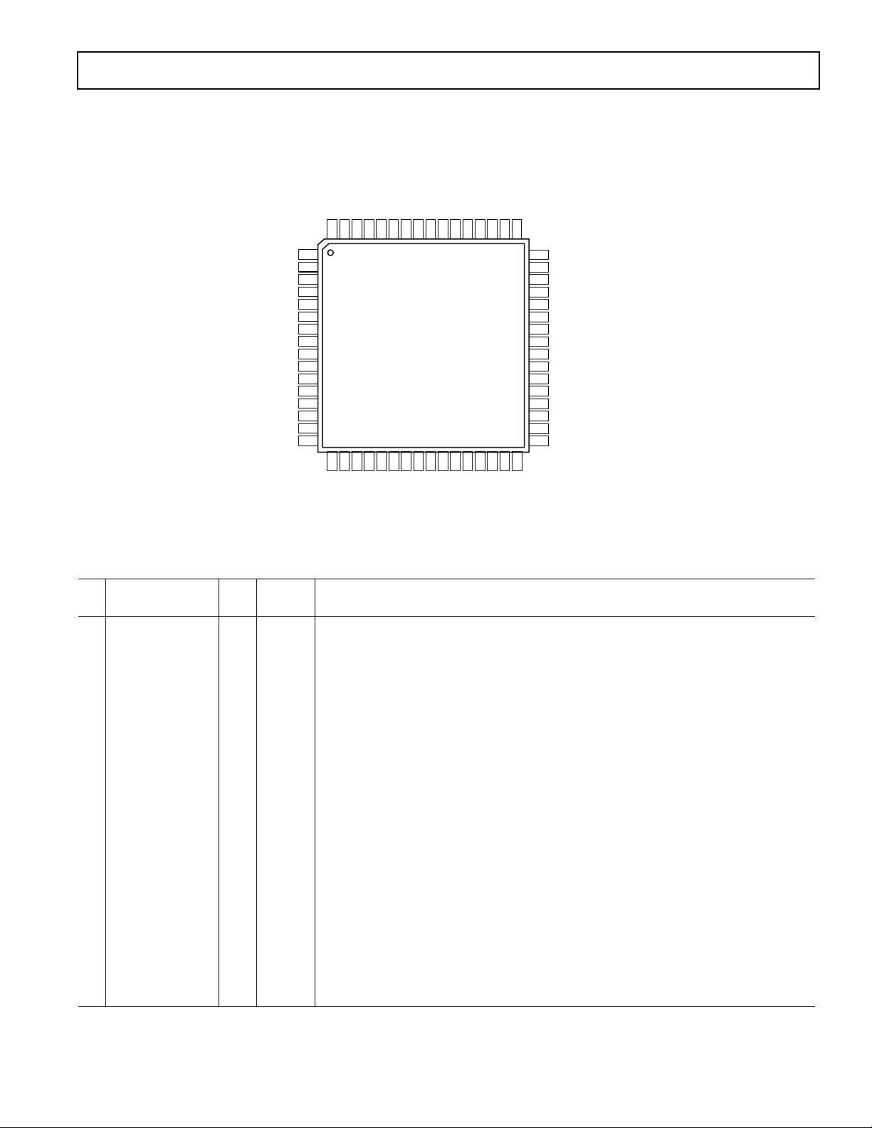
PIN CONFIGURATION
OPT2–
OPT1–
POWERONKEY–
ISENSE
ADPSUPPLY
ADAPTER
BASE
MVBAT
AGND
NRCAP
BVS
LDO10 (RF OPTION)
VBAT
LDO9 (RF Rx2)
AGND
LDO8 (RF Tx)
64
63
62
61
60
59
58
57
56
55
54
53
52
51
50
49
1
2
3
4
5
6
7
8
9
10
11
12
13
14
15
16
17
18
RTCV
OSC IN
19
20
AGND
OSC OUT
ADP3502
TOP VIEW
(Not to Scale)
21
22
23
GPIO0
GPIO1
GPIO2
24
25
DATA
GPIO3
26
CS
27
28
CLKIN
RESETIN–
29
32K OUT
30
31
RESET+
RESETOUT–
48
VBAT
47
LDO7 (REF Rx1)
46
LDO6 (BASEBAND CORE)
45
VBAT
44
LDO5 (VIBRATOR)
43
LDO4 (AUDIO)
42
VBAT
41
LDO2 (BASEBAND AVDD)
40
REFO
39
AGND
38
LDO3 (RTC/COIN-CELL)
37
VBAT
36
LDO1 (BASEBAND VDD)
35
LDO11 (OPTION)
34
VBAT
33
RSTDELAY–
32
TEST
PIN FUNCTION DESCRIPTION
Pin
No. Mnemonic I/O Supply Function
1 OPT3 I VBAT Optional Power ON Input. ADP3502 will keep power ON when this pin goes high.
2 KEYPADCOL0 O LDO1 Keypad Column Strobe 0 (Open-Drain, Pull Low)
3 KEYPADCOL1 O LDO1 Keypad Column Strobe 1 (Open-Drain, Pull Low)
4 KEYPADCOL2 O LDO1 Keypad Column Strobe 2 (Open-Drain, Pull Low)
5 KEYPADCOL3 O LDO1 Keypad Column Strobe 3 (Open-Drain, Pull Low)
6 KEYPADROW0 I LDO1 Keypad Row Input 0. Pulled up internally, 20 kΩ.
7 KEYPADROW1 I LDO1 Keypad Row Input 1. Pulled up internally, 20 kΩ.
8 KEYPADROW2 I LDO1 Keypad Row Input 2. Pulled up internally, 20 kΩ.
9 KEYPADROW3 I LDO1 Keypad Row Input 3. Pulled up internally, 20 kΩ.
10 KEYPADROW4 I LDO1 Keypad Row Input 4. Pulled up internally, 20 kΩ.
11 KEYPADROW5 I LDO1 Keypad Row Input 5. Pulled up internally, 20 kΩ.
12 TCXOON I LDO1 Logic Input Pin for Main LDOs (LDO1, LDO2, LDO3, LDO6) Turning On Control.
L: OFF, H: ON.
13 SLEEP– I LDO1 Logic Input Pin for LDO7 and LDO9. This input gates register data for these LDOs.
LDO7 and LDO9 are turned OFF when SLEEP goes low even if the registers are set
to ON. If register of SLEEP7 and SLEEP9 are set to “1,” the SLEEP signal is ignored.
14 BLIGHT O VBAT LED Drive. Open-drain output.
15 DGND Digital Ground
16 INT– O LDO1 Interrupt Signal Output
REV. 0
–9–

ADP3502
PIN FUNCTION DESCRIPTION (continued)
Pin
No. Mnemonic I/O Supply Function
17 RTCV Supply input for RTC, 32 kHz OSC, and other logic. Connects to coin cell battery in
typical operation.
18 OSC IN RTCV Connect to 32.768 kHz crystal
19 AGND Analog Ground
20 OSC OUT RTCV Connect to 32.768 kHz crystal
21 GPIO0 I/O LDO1 General-purpose input and output port. Integrated interrupt function. Interrupt occurs
on both the falling and rising edges.
22 GPIO1 I/O LDO1 General-purpose input and output port. Integrated interrupt function. Interrupt occurs
on both the falling and rising edges.
23 GPIO2 I/O LDO1 General-purpose input and output port. Integrated interrupt function. Interrupt occurs
on both the falling and rising edges.
24 GPIO3 I/O LDO1 General-purpose input and output port. Integrated interrupt function. Interrupt occurs
on both the falling and rising edges.
25 DATA I/O LDO1 Serial interface data input and output
26 CS I LDO1 Serial interface chip select input. Active high input.
27 CLKIN I LDO1 Serial interface clock input
28 RESETIN– I LDO1 Reset input signal for internal reset signal; Starts stay-alive timer.
29 32K OUT O RTCV 32.768 kHz output. Output after 30 ms when reset is released.
30 RESET+ O RTCV Reset output. Invert signal of RESETOUT–. Open-drain and low leakage.
31 RESETOUT– O RTCV Reset output. Follows voltage detector operation. Open-drain output.
32 TEST I RTCV
33 RSTDELAY– O RTCV Reset output. 50 ms delayed. Connect to baseband’s reset input in typical application.
34 VBAT Supply input. Connect to battery.
35 LDO11 O VBAT Regulator No. 11 output. General-purpose supply.
36 LDO1 O VBAT Regulator No. 1 output. Use for baseband I/O supply.
37 VBAT Supply input. Connect to battery.
38 LDO3 O VBAT Regulator No. 3 output. If VBAT > 2.7 V, the output is always active. Use for coin cell supply.
39 AGND Analog ground
40 REFO O VBAT Output of LDO2 through FET switch
41 LDO2 O VBAT Regulator No. 2 output. Use for baseband analog supply.
42 VBAT Supply input. Connect to battery.
43 LDO4 O VBAT Regulator No. 4 output. Use for general analog supplies, for example, speaker amp.
44 LDO5 O VBAT Regulator No. 5 output. Use for vibrator.
45 VBAT Supply input. Connect to battery.
46 LDO6 O VBAT Regulator No. 6 output. Use for baseband core supply.
47 LDO7 O VBAT Regulator No. 7 output. Use for RF Rx IC supply. Gated with SLEEP– signal input.
48 VBAT Supply input. Connect to battery.
49 LDO8 O VBAT Regulator No. 8 output. Use for RF Tx IC supply.
50 AGND Analog Ground
51 LDO9 O VBAT Regulator No. 9 output. Use for RF Rx IC supply. Gated with SLEEP– input signal.
52 VBAT Supply input. Connect to battery.
53 LDO10 O VBAT Regulator No. 10 output. General-purpose supply.
Test pin. Reserved for ADI use. Connect to GND for normal operation.
Open-drain output.
REV. 0–10–

ADP3502
PIN FUNCTION DESCRIPTION (continued)
Pin
No. Mnemonic I/O Supply Function
54 BVS Battery voltage sense input for charger. Connect to battery with a separate low current
trace
55 NRCAP O VBAT Noise reduction capacitor, 0.1 µF MLCC
56 AGND Analog Ground
57 MVBAT O VBAT Battery voltage divider output. Buffered internally. Connect to baseband ADC.
58 BASE O ADAPTER Base drive output for PNP pass transistor
59 ADAPTER AC Adapter Input
60 ADPSUPPLYI ADAPTER Supply bias current to charging related blocks
61 ISENSE I ADAPTER Charge current sense input
62 PWRONKEY– I VBAT Power ON/OFF key input. Pulled up internally with 140 kΩ.
63 OPT1– I VBAT Optional power ON input. ADP3502 will keep power on when this pin goes low.
64 OPT2– I/O VBAT Optional power ON input. ADP3502 will keep power on when this pin goes low.
While the part is powered up, the input is pulled low (GND) internally. Do not connect to any supply or signal source.
REV. 0
–11–
 Loading...