

Analog Devices ADP3410 a Datasheet
Dual MOSFET Driver
V
CC
V
CC
CONTROL
AND
OVERLAP
PROTECTION
CIRCUIT
ADP3410
4.4V
1.2V
VCC
VCCGD
GND
SD
IN
DLY
OVPSET
DRVLSD
PGND
BST
DRVH
SW
DRVL
SRMON
a
FEATURES
All-In-One Synchronous Buck Driver
One PWM Signal Generates Both Drives
Anticross-Conduction Protection Circuitry
Programmable Transition Delay
Synchronous Override Control
Undervoltage Lockout
Programmable Overvoltage Shutdown
Good Signal Drives Auxiliary Circuits
V
CC
Shutdown Quiescent Current < 10 A
APPLICATIONS
Mobile Computing CPU Core Power Converters
Multiphase Desktop CPU Supplies
Single-Supply Synchronous Buck Converters
Standard-to-Synchronous Converter Adaptations
with Bootstrapping
ADP3410
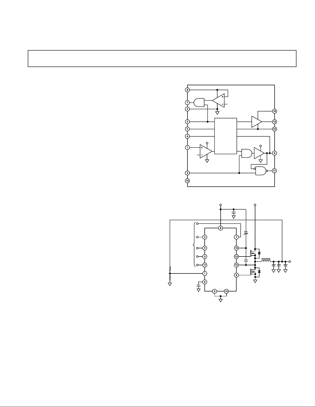
FUNCTIONAL BLOCK DIAGRAM
GENERAL DESCRIPTION
5V
V
BATT
The ADP3410 is a dual MOSFET driver optimized for driving
two N-channel FETs that are the two switches in the nonisolated synchronous buck power converter topology. Each of
the drivers is capable of driving a 3000 pF load with a 20 ns
propagation delay and a 30 ns transition time. One of the drivers
can be bootstrapped, and is designed to handle the high-voltage
slew rate associated with “floating” high-side gate drivers. The
ADP3410 has several protection features: overlapping drive
prevention (ODP), undervoltage lockout (UVLO) with performance specified at very low VCC levels, and overvoltage protection
(OVP) that can be used to monitor either the input or output.
Additional features include: programmable transition delay, a
synchronous drive override control pin, a synchronous drive
status monitor and, in conjunction with exiting from the UVLO
mode, a V
Good (VCCGD) signal capable of driving a 10 mA
CC
TO PWM
CONTROLLER
VCC
SD
ADP3410
IN
DRVLSD
SRMON
OVPSET
DLY
GND PGND
VCCGD
BST
DRVH
SW
DRVL
V
OUT
load. The quiescent current, when the device is disabled, is less
than 10 mA.
REV. A
Information furnished by Analog Devices is believed to be accurate and
reliable. However, no responsibility is assumed by Analog Devices for its
use, nor for any infringements of patents or other rights of third parties
that may result from its use. No license is granted by implication or
otherwise under any patent or patent rights of Analog Devices.
One Technology Way, P.O. Box 9106, Norwood, MA 02062-9106, U.S.A.
Tel: 781/329-4700www.analog.com
Fax: 781/326-8703 © Analog Devices, Inc., 2002
Figure 1. Typical Application Circuit

(TA = 0ⴗC to 85ⴗC, VCC = 5 V, VBST = 4 V to 26 V, SD > 2 V, unless otherwise
1
ADP3410–SPECIFICATIONS
noted.)
Parameter Symbol Conditions Min Typ Max Unit
SUPPLY
Supply Voltage Range V
Quiescent Current I
CC
CCQ
4.15 5.0 6.0 V
Shutdown Mode VSD < 0.8 V 10 mA
Operating Mode VSD > 2.0 V, No Switching 1 2 mA
VCCGD OUTPUT
Output Voltage High VCC = 4.6 V, I
Output Voltage Low V
VCCGD Propagation Delay
(See Figure 4) tpdl
2, 3
tpdh
, SD Goes High 10 ms
VCCGD
VCCGD
< UVLO, I
CC
SD Goes Low 10 ms
= 10 mA 4.5 4.55 V
LOAD
= 10 mA 0.1 0.2 V
LOAD
SYNCHRONOUS RECTIFIER
MONITOR
Output Voltage High 4.15 V
Output Voltage Low V
Transition Time
Propagation Delay
2
2, 3
tr
SRMON, tfSRMONVCC
tpdh
SRMON
= 4.6 V, C
CC
= 4.6 V, C
DRVLSD Is High and 15 ns
= 100 pF 50 mV
LOAD
= 100 pF 20 ns
LOAD
DRVL Goes High, or
DRVLSD Goes Low
tpdl
SRMON
DRVLSD Is High and 15 ns
DRVL Goes Low
UNDERVOLTAGE LOCKOUT
UVLO Threshold 4.2 4.4 4.6 V
UVLO Hysteresis 0.05 V
UVLO Logic Active Threshold 1.5 V
Propagation Delay
UVLO
(See Figure 5) tpdl
2, 3
tpdh
UVLO
UVLO
VCC Goes High 10 ms
VCC Goes Low 10 ms
OVERVOLTAGE PROTECTION
Trip Threshold 1.145 1.2 1.255 V
Hysteresis 0.8 V
Bias Current 0.2 1.0 mA
OVP Propagation Delay
2, 3, 4
tpdh
OVP
VCC = 4.6 V, OVPSET Goes High 0.5 ms
SYNCHRONOUS RECTIFIER ENABLE
DRVLSD
Input Voltage High
Input Voltage Low
Propagation Delay
(See Figure 3) tpdh
SD INPUT
Input Voltage High
Input Voltage Low
PWM INPUT (IN)
Input Voltage High
Input Voltage Low
5
2, 3
5
5
5
2.0 V
0.8 V
tpdl
5
,VCC = 4.6 V, 30 ns
DRVLSD
DRVLSD
C
LOAD (DRVL)
= 3 nF
2.0 V
0.8 V
5
2.0 V
0.8 V
THERMAL SHUTDOWN
Overtemperature Trip Point 165 ∞C
OTP Hysteresis 10 ∞C
HIGH-SIDE DRIVER
Output Resistance, Sourcing Current V
Output Resistance, Sinking Current V
DRVH Transition Times
(See Figure 6) tf
DRVH Propagation Delay
(See Figure 6) tpdl
2
2, 3, 6
tr
,V
DRVH
DRVH
tpdh
,V
DRVH
DRVH
– VSW = 4.6 V 2.5 5 W
BST
– VSW = 4.6 V 2.5 5 W
BST
– V
BST
BST
= 4.6 V, C
SW
– VSW = 4.6 V 10 20 ns
= 3 nF 20 35 ns
LOAD
25 ns
–2–
REV. A

ADP3410
WARNING!
ESD SENSITIVE DEVICE
Parameter Symbol Conditions Min Typ Max Unit
LOW-SIDE DRIVER
Output Resistance, Sourcing Current V
Output Resistance, Sinking Current V
DRVL Transition Times
(See Figure 6) tf
DRVL Propagation Delay
(See Figure 6) tpdl
NOTES
1
All limits at temperature extremes are guaranteed via correlation using standard Statistical Quality Control (SQC) methods.
2
AC specifications are guaranteed by characterization, but not production tested.
3
For propagation delays, tpdh refers to the specified signal going high, tpdl refers to it going low.
4
Propagation delay measured until DRVL begins its transition.
5
Logic inputs meet typical CMOS I/O conditions for source/sink current (~1 mA).
6
Maximum propagation delay = 40 ns max + (1 ns/pF ¥ C
Specifications subject to change without notice.
2
2, 3
tr
DRVL,
DRVL
tpdh
DLY
DRVL
DRVL
).
= 4.6 V 2.5 5 W
CC
= 4.6 V 2.5 5 W
CC
VCC = 4.6 V, C
= 3 nF 20 35 ns
LOAD
VCC = 4.6 V 5 30 ns
25 ns
ABSOLUTE MAXIMUM RATINGS*
ORDERING GUIDE
VCC to PGND . . . . . . . . . . . . . . . . . . . . . . . . –0.3 V to +7 V
BST to PGND . . . . . . . . . . . . . . . . . . . . . . . . –0.3 V to +30 V
BST to SW . . . . . . . . . . . . . . . . . . . . . . . . . . . –0.3 V to +7 V
SW to PGND . . . . . . . . . . . . . . . . . . . . . . . . –2.0 V to +25 V
Model Temperature Package Package
Range Description Option
ADP3410KRU 0∞C to 85∞CThin Shrink Small RU-14
OVPSET to PGND . . . . . . . . . . . . . . . . . . . . –0.3 V to +10 V
SD, IN, DRVLSD to GND . . . . . . . . . . . . . . –0.3 V to +7.3 V
GND to PGND . . . . . . . . . . . . . . . . . . . . . . . . . . . . . . ±0.3 V
Operating Ambient Temperature Range . . . . . . . 0∞C to 85∞C
Operating Junction Temperature Range . . . . . . 0∞C to 125∞C
. . . . . . . . . . . . . . . . . . . . . . . . . . . . . . . . . . . . 155∞C/W
q
JA
q
. . . . . . . . . . . . . . . . . . . . . . . . . . . . . . . . . . . . . 40∞C/W
JC
Storage Temperature Range . . . . . . . . . . . . –65∞C to +150∞C
Lead Temperature (Soldering, 10 sec) . . . . . . . . . . . . . 300∞C
*This is a stress rating only; operation beyond these limits can cause the device to
be permanently damaged.
CAUTION
ESD (electrostatic discharge) sensitive device. Electrostatic charges as high as 4000 V readily
accumulate on the human body and test equipment and can discharge without detection.
Although the ADP3410 features proprietary ESD protection circuitry, permanent damage may
occur on devices subjected to high-energy electrostatic discharges. Therefore, proper ESD
precautions are recommended to avoid performance degradation or loss of functionality.
Outline Package
(TSSOP-14)
REV. A
–3–
ADP3410
PIN FUNCTION DESCRIPTIONS
Pin Mnemonic Function
1 OVPSET Overvoltage Shutdown Sense Input. Shutdown occurs when this pin is driven above the specified thresh-
old. It is a high-impedance comparator input, so an external resistor divider can be used to scale the
controlling voltage for OVP.
2 SD Shutdown. When high, this pin enables normal operation. When low, VCCGD, DRVH, and DRVL are
forced low and the supply current (ICC
3GND Signal Ground. The input signal and the capacitor at DLY should be closely referenced to this ground.
4IN TTL-level input signal which has primary control of the drive outputs.
5 DRVLSD Synchronous Rectifier Enable. When low, this signal forces DRVL low. The propagation delay time is on
the order of that for the main input signal, so it can be used for real time modulation control of DRVL.
When DRVLSD is high, DRVL is enabled and controlled by IN.
6 DLY Low-High-Transition Delay. A capacitor from this pin to ground programs the propagation delay
from turn-off of the lower FET to turn-on of the upper FET. The formula for the low-high-transition
delay is DLY = C
¥ (1 ns/pF) + 20 ns. The rise time for turn-on of the upper FET is not included in
DLY
the formula.
7 VCCGD V
Good. This pin indicates the status of the undervoltage lockout. When VCC is high enough for the
CC
device to exit UVLO mode, the VCCGD pin is pulled up to V
signal is capable of acting as a switched power rail for external circuitry, since it can source 10 mA and
sink 10 mA.
8 VCC Input Supply. This pin should be bypassed to PGND with ~1 mF ceramic capacitor.
9 DRVL Synchronous Rectifier Drive. Output drive for the lower (synchronous rectifier) FET.
10 PGND Power Ground. Should be closely connected to the source of the lower FET.
11 SRMON Synchronous Rectifier Monitor. When DRVLSD is high, SRMON follows DRVL. When DRVLSD is
low, SRMON is high. TTL-type output.
12 SW This pin is connected to the buck switching node, close to the upper FET’s source. It is the floating return
for the upper FET drive signal. Also, it is used to monitor the switched voltage to prevent turn-on of the
lower FET until the voltage is below ~1 V. Thus, the high-low-transition delay is determined at this pin
according to operating conditions. This pin can be subjected to voltages as low as 2 V below PGND.
13 DRVH Buck Drive. Output drive for the upper (buck) FET.
14 BST Floating Bootstrap Supply for the upper FET. A capacitor connected between BST and SW pins holds
this bootstrapped voltage for the high-side FET as it is switched. The capacitor should be chosen between
0.1 mF and 1 mF.
) is minimized as specified.
Q
CC
with the specified low impedance. This
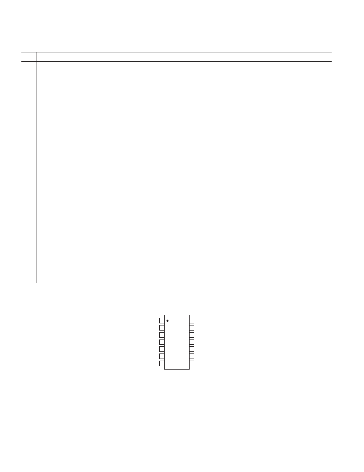
PIN CONFIGURATION
1
OVPSET
GND
DRVLSD
DLY
VCCGD
SD
IN
2
3
ADP3410
4
TOP VIEW
5
(Not to Scale)
6
7
14
13
12
11
10
9
8
BST
DRVH
SW
SRMON
PGND
DRVL
VCC
–4–
REV. A
 Loading...