

Analog Devices ADP3401 Datasheet
a
DIGITAL
LDO
VCC
VRTC
VTCXO
PWRONKEY
ROWX
PWRONIN
RESET
ANALOGON
POWER-UP
SEQUENCING
AND
PROTECTION
LOGIC
ADP3401
VBAT
REFOUT
AGND
VCCA
RESCAP
CHRON
SIMBAT
CAP+
CAP2
SIMPROG
SIMON
SIMGND
RESETIN
CLKIN
DATAIO
CHARGE
PUMP
LOGIC LEVEL
TRANSLATION
BUFFER
REF
+
I/O
RSTCLK
VSIM
RTC LDO
XTAL OSC
LDO
ANALOG
LDO
DGND
GSM Power Management System
ADP3401
FEATURES
Handles all GSM Baseband Power Management
Functions
Four LDOs Optimized for Specific GSM Subsystems
Charges Li-Mn Coin Cell for Real-Time Clock
Charge Pump and Logic Level Translators for 3 V and 5 V
GSM SIM Modules
Thermally Enhanced 6.1 mm 28-Lead TSSOP Package
APPLICATIONS
GSM/DCS/PCS Handsets
TeleMatic Systems
ICO/Iridium Terminals
GENERAL DESCRIPTION
The ADP3401 is a multifunction power management system IC
optimized for GSM cell phones. The wide input voltage range of
3.0 V to 7.0 V makes the ADP3401 ideal for both single cell Li-Ion
and three cell NiMH designs. The current consumption of the
ADP3401 has been optimized for maximum battery life, featuring
a ground current of only 150 µA when the phone is in standby
(digital LDO, and SIM card supply active). An undervoltage lockout (UVLO) prevents the startup when there is not enough energy
in the battery. All four integrated LDOs are optimized to power
one of the critical sub-blocks of the phone. Their novel anyCAP™
architecture requires only very small output capacitors for stability,
and the LDOs are insensitive to the capacitors’ equivalent series
resistance (ESR). This makes them stable with any capacitor,
including ceramic (MLCC) types for space-restricted applications.
A step-up converter is implemented to supply both the SIM
module and the level translation circuitry to adapt logic signals
for 3 V and 5 V SIM modules. Sophisticated controls are available for power-up during battery charging, keypad interface, and
charging of an auxiliary backup battery for the real-time clock.
These allow an easy interface between ADP3401, GSM processor, charger, and keypad. The 28-lead TSSOP package has been
thermally enhanced to maximize power dissipation capability.
Furthermore, a reset circuit and a thermal shutdown function
have been implemented to support reliable system design.
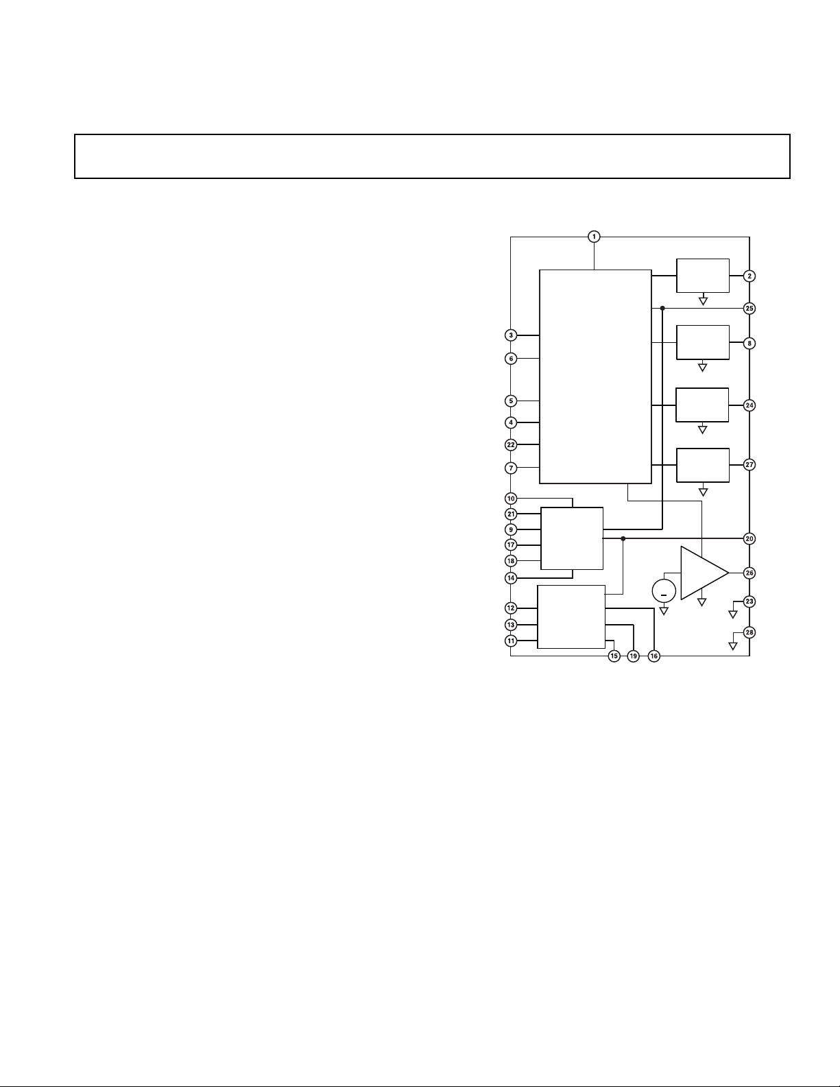
FUNCTIONAL BLOCK DIAGRAM
anyCAP is a trademark of Analog Devices, Inc.
REV. 0
Information furnished by Analog Devices is believed to be accurate and
reliable. However, no responsibility is assumed by Analog Devices for its
use, nor for any infringements of patents or other rights of third parties
which may result from its use. No license is granted by implication or
otherwise under any patent or patent rights of Analog Devices.
One Technology Way, P.O. Box 9106, Norwood, MA 02062-9106, U.S.A.
Tel: 781/329-4700 World Wide Web Site: http://www.analog.com
Fax: 781/326-8703 © Analog Devices, Inc., 2000

ADP3401–SPECIFICATIONS
(–20°C ≤ TA ≤ +85°C, VBAT = 3 V to 7 V, C
C
= C
VCC
= 2.2 F, C
VCCA
= 0.1 F, C
VRTC
VBAT
= 0.22 F, C
VTCXO
= C
SIMBAT
= C
= 10 F,
VSIM
= 0.1 F, min. loads applied
VCAP
on all outputs, unless otherwise noted)
ELECTRICAL CHARACTERISTICS
1
Parameter Symbol Conditions Min Typ Max Unit
SHUTDOWN SUPPLY CURRENT I
BAT
VBAT = Low (UVLO Low) VBAT = 2.7 V 3 20 µA
VBAT = High (UVLO High) VBAT
OPERATING GROUND CURRENT I
GND
VCC and VRTC On Minimum Loads, VBAT
VCC, VRTC and VSIM On Minimum Loads, VBAT
All LDOs and VSIM On Minimum Loads, VBAT
= 3.6 V, VRTC On 12 30 µA
= 3.6 V 100 140 µA
= 3.6 V 150 240 µA
= 3.6 V 260 400 µA
All LDOs and VSIM On Maximum Loads, VBAT = 3.6 V 15 mA
UVLO CHARACTERISTICS
UVLO On Threshold VBAT
UVLO
3.0 3.3 V
UVLO Hysteresis 100 mV
INPUT CHARACTERISTICS
Input High Voltage V
IH
PWRONIN and ANALOGON 2 V
PWRONKEY 0.7 ⫻ VBAT V
Input Low Voltage V
IL
PWRONIN and ANALOGON 0.4 V
PWRONKEY 0.3 ⫻ VBAT V
PWRONKEY INPUT PULL-UP
RESISTANCE TO VBAT 15 20 25 kΩ
CHRON CHARACTERISTICS
CHRON Threshold V
CHRON Hysteresis Resistance R
CHRON Input Bias Current I
T
IN
B
2.38 < CHRON < V
CHRON > V
T
T
2.38 2.48 2.58 V
108 125 138 kΩ
0.5 µA
ROWX CHARACTERISTICS
ROWX Output Low Voltage V
ROWX Output High Leakage I
OL
IH
PWRONKEY = Low 0.4 V
= 200 µA
I
OL
PWRONKEY = High 1 µA
Current V(ROWX) = 5 V
SHUTDOWN
Thermal Shutdown Threshold
2
Junction Temperature 160 ºC
Thermal Shutdown Hysteresis Junction Temperature 35 ºC
DIGITAL LDO (VCC)
Output Voltage VCC Line, Load, Temp 2.710 2.765 2.820 V
Line Regulation DVCC 3 V < VBAT < 7 V, Min Load 2 mV
Load Regulation DVCC 50 µA < I
Output Capacitor
3
Dropout Voltage V
C
O
DO
VBAT = 3.6 V
VO = V
I
= 100 mA
LOAD
< 100 mA, 15 mV
LOAD
2.2 µF
– 100 mV 215 mV
INITIAL
ANALOG LDO (VCCA)
Output Voltage VCCA Line, Load, Temp 2.710 2.765 2.820 V
Line Regulation DVCCA 3 V < VBAT < 7 V, Min Load 2 mV
Load Regulation DVCCA 200 µA < I
Output Capacitor
3
Dropout Voltage V
C
O
DO
VBAT = 3.6 V
VO = V
INITIAL
= 130 mA
I
LOAD
< 130 mA, 15 mV
LOAD
2.2 µF
– 100 mV 215 mV
Ripple Rejection DVBAT/ f = 217 Hz (t = 4.6 ms) 65 70 dB
DVCCA VBAT = 3.6 V
Output Noise Voltage V
NOISE
f = 10 Hz to 100 kHz 75 µV rms
I
= 130 mA, VBAT = 3.6 V
LOAD
–2– REV. 0

ADP3401
Parameter Symbol Conditions Min Typ Max Unit
CRYSTAL OSCILLATOR LDO (VTCXO)
Output Voltage VTCXO Line, Load, Temp 2.710 2.765 2.820 V
Line Regulation ∆VTCXO 3 V < VBAT < 7 V, Min Load 2 mV
Load Regulation ∆VTCXO 100 µA < I
Output Capacitor
3
Dropout Voltage V
C
O
DO
VBAT = 3.6V
VO = V
INITIAL
= 5 mA
I
LOAD
Ripple Rejection ∆VBAT/ f = 217 Hz (t = 4.6 ms) 65 72 dB
∆VTCXO VBAT = 3.6 V
Output Noise Voltage V
NOISE
f = 10 Hz to 100 kHz 80 µV rms
I
= 5 mA, VBAT = 3.6 V
LOAD
VOLTAGE REFERENCE (REFOUT)
Output Voltage V
Line Regulation ∆V
REFOUT
REFOUT
Line, Load, Temp 1.192 1.210 1.228 V
3 V < VBAT < 7 V, Min Load 2 mV
< 5 mA, 1 mV
LOAD
0.22 µF
– 100 mV 150 mV
Load Regulation ∆V
REFOUT
0 µA < I
< 50 µA, 0.5 mV
LOAD
VBAT = 3.6 V
Ripple Rejection ∆VBAT/ f = 217 Hz (t = 4.6 ms), 65 75 dB
VBAT = 3.6 V
100 pF
f = 10 Hz to 100 kHz 40 µV rms
Maximum Capacitive Load C
Output Noise Voltage V
∆V
O
NOISE
REFOUT
VBAT = 3.6 V
REAL-TIME CLOCK LDO/
BATTERY CHARGER (VRTC)
Maximum Output Voltage VRTC I
Current Limit I
Off Reverse Leakage
Current
Dropout Voltage V
MAX
I
L
DO
≤ 10 µA 2.810 2.850 2.890 V
LOAD
3.050 V < VBAT < 7 V 175 µA
2.0 V < VBAT < UVLO 1 µA
VO = V
I
LOAD
= 10 µA
– 10 mV 170 mV
INITIAL
SIM CHARGE PUMP (VSIM)
Output Voltage for 5 V SIM Modules VSIM 0 mA ≤ I
≤ 10 mA 4.70 5.00 5.30 V
LOAD
SIMPROG = High
Output Voltage for 3 V SIM Modules VSIM 0 mA ≤ I
≤ 6 mA 2.82 3.00 3.18 V
LOAD
SIMPROG = Low
GSM/SIM LOGIC TRANSLATION
(GSM INTERFACE)
Input High Voltage (SIMPROG, SIMON, V
IH
VCC – 0.6 V
RESETIN, CLKIN)
Input Low Voltage (SIMPROG, SIMON, V
IL
0.6 V
RESETIN, CLKIN)
DATAIO V
DATAIO Pull-Up Resistance to VCC R
IL
, V
V
IH
OH
I
IL
V
OL
IN
VOL(I/O) = 0.4 V, 0.230 V
(I/O) = 1 mA
I
OL
(I/O) = 0.4 V, 0.335 V
V
OL
(I/O ) = 0 mA
I
OL
IIH, I
= ±10 µA VCC
OH
– 0.4 V
VIL = 0 V –0.9 mA
VIL (I/O) = 0.4 V 0.420 V
16 20 24 kΩ
–3–REV. 0

ADP3401
Parameter Symbol Conditions Min Typ Max Unit
SIM INTERFACE
VSIM = 5 V
RST V
RST V
CLK V
CLK V
I/O V
I/O V
I/O I
I/O V
OL
OH
OL
OH
IL
, V
IH
OH
IL
OL
VSIM = 3 V
RST V
RST V
CLK V
CLK V
I/O V
I/O V
I/O I
I/O V
I/O Pull-Up Resistance to VSIM R
Max Frequency (CLK) f
Prop Delay (CLK) t
Output Rise/Fall Times (CLK) t
Output Rise/Fall Times (I/O, RST) t
OL
OH
OL
OH
IL
IH
IL
OL
IN
MAX
D
, t
R
, t
R
, V
F
F
OH
Duty Cycle (CLK) D D CLKIN = 50% 47 53 %
RESET GENERATOR (RESET)
Output High Voltage V
Output Low Voltage V
Delay Time Per Unit Capacitance t
OH
OL
D
Applied to RESCAP Pin
NOTES
1
All limits at temperature extremes are guaranteed via correlation using standard Statistical Quality Control (SQC) methods .
2
This feature is intended to protect against catastophic failure of the device. Maximum allowed operating junction temperature is 125ºC. Operation beyond 125ºC
could cause permenant damage to the device.
3
Required for stability.
Specifications subject to change without notice.
I = +200 µA 0.6 V
I = –20 µA VSIM
– 0.7 V
I = +200 µA 0.5 V
I = –20 µA 0.7 ⫻ VSIM V
0.4 V
IIH, I
= ±20 µA VSIM – 0.4 V
OH
VIL = 0 V –0.9 mA
IOL = +1 mA 0.4 V
DATAIO ≤ 0.23 V
I = +200 µA 0.2 ⫻ VSIM V
I = –20 µA 0.8 ⫻ VSIM V
I = +20 µA 0.2 ⫻ VSIM V
I = –20 µA 0.7 ⫻ VSIM V
0.4 V
IIH, I
= ±20 µA VSIM – 0.4 V
OH
VIL= 0 V –0.9 mA
IOL = 1 mA 0.4 V
DATAIO ≤ 0.23 V
81012kΩ
CL = 30 pF 5 MHz
30 50 ns
CL = 30 pF 9 18 ns
C
= 30 pF 1 µs
L
f = 5 MHz
I
= –15 µA VCC – 0.3 V
OH
I
= –15 µA 0.3 V
OL
1.0 ms/nF
–4– REV. 0
 Loading...