Analog Devices ADP3336 Datasheet

High Accuracy Ultralow IQ, 500 mA
THERMAL
PROTECTION
CC
IN
ADP3336
OUT
GND
Q1
BANDGAP
REF
DRIVER
g
m
FB
SD
a
anyCAP
®
Adjustable Low Dropout Regulator
FEATURES
High Accuracy Over Line and Load: ⴞ0.9% @ 25ⴗC,
ⴞ1.8% Over Temperature
Ultralow Dropout Voltage: 200 mV (Typ) @ 500 mA
Requires Only C
= 1.0 F for Stability
O
anyCAP = Stable with Any Type of Capacitor
(Including MLCC)
Current and Thermal Limiting
Low Noise
Low Shutdown Current: < 1.0 A
2.6 V to 12 V Supply Range
1.5 V to 10 V Output Range
–40ⴗC to +85ⴗC Ambient Temperature Range
Ultrasmall Thermally-Enhanced 8-Lead MSOP Package
APPLICATIONS
PCMCIA Card
Cellular Phones
Camcorders, Cameras
Networking Systems, DSL/Cable Modems
Cable Set-Top Box
MP3/CD Players
DSP Supply
GENERAL DESCRIPTION
The ADP3336 is a member of the ADP333x family of precision
low dropout anyCAP voltage regulators. The ADP3336 operates
with an input voltage range of 2.6 V to 12 V and delivers a
continuous load current up to 500 mA. The ADP3336 stands
out from conventional LDOs with the lowest thermal resistance
of any MSOP-8 package and an enhanced process that enables
it to offer performance advantages beyond its competition.
Its patented design requires only a 1.0 µF output capacitor for
stability. This device is insensitive to output capacitor Equivalent Series Resistance (ESR), and is stable with any good
quality capacitor, including ceramic (MLCC) types for spacerestricted applications. The ADP3336 achieves exceptional
accuracy of ±0.9% at room temperature and ±1.8% over temperature, line, and load. The dropout voltage of the ADP3336 is
only 200 mV (typical) at 500 mA. This device also includes a
safety current limit, thermal overload protection and a shutdown
feature. In shutdown mode, the ground current is reduced to
less than 1 µA. The ADP3336 has ultralow quiescent current
80 µA (typical) in light load situations.
ADP3336
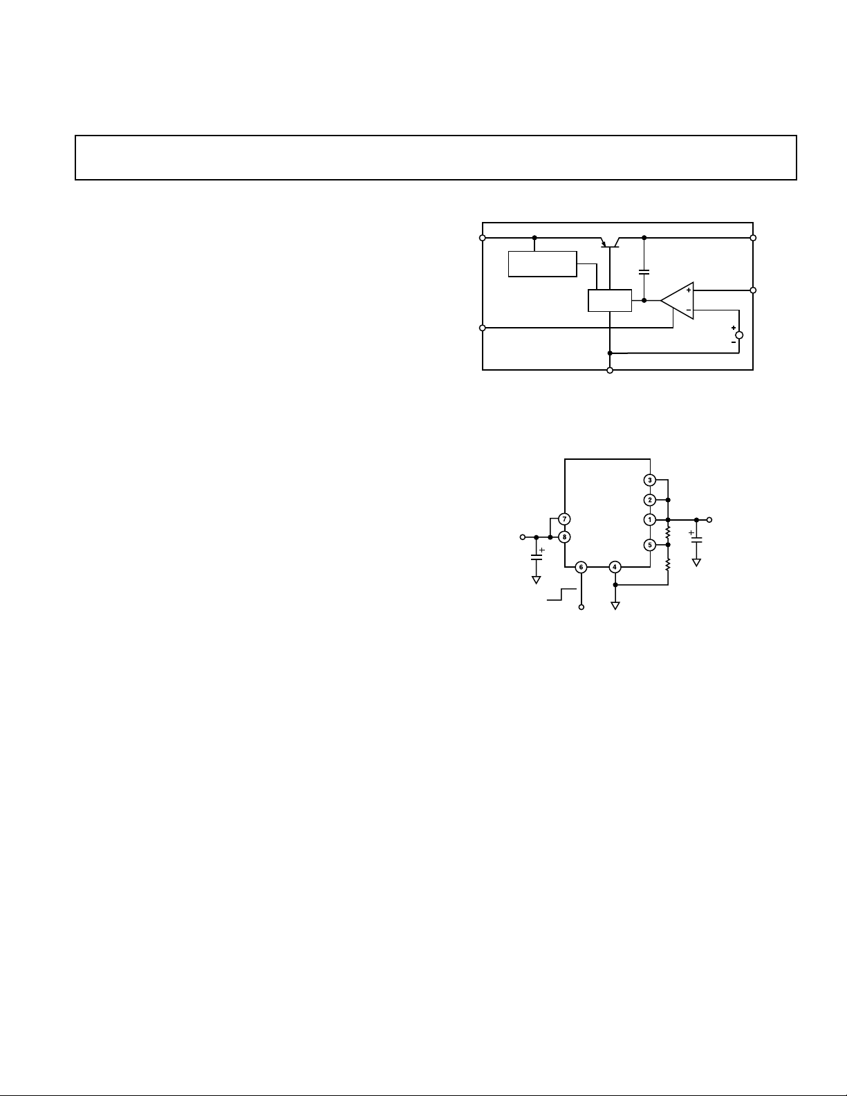
FUNCTIONAL BLOCK DIAGRAM
ADP3336
OUT
OUT
IN
V
IN
C
IN
1F
OFF
IN
SD
ON
Figure 1. Typical Application Circuit
GND
OUT
R1
FB
R2
C
1F
V
OUT
OUT
anyCAP is a registered trademark of Analog Devices Inc.
REV. 0
Information furnished by Analog Devices is believed to be accurate and
reliable. However, no responsibility is assumed by Analog Devices for its
use, nor for any infringements of patents or other rights of third parties
which may result from its use. No license is granted by implication or
otherwise under any patent or patent rights of Analog Devices.
One Technology Way, P.O. Box 9106, Norwood, MA 02062-9106, U.S.A.
Tel: 781/329-4700 World Wide Web Site: http://www.analog.com
Fax: 781/326-8703 © Analog Devices, Inc., 2000

1, 2
ADP3336–SPECIFICATIONS
(VIN = 6.0 V, CIN = C
Parameter Symbol Conditions Min Typ Max Unit
OUTPUT
Voltage Accuracy
Line Regulation
Load Regulation I
Dropout Voltage V
3, 4
3
V
OUT
DROP
VIN = V
I
T
V
I
T
V
I
T
VIN = V
I
T
T
V
OUT(NOM)
= 0.1 mA to 500 mA
L
= 25°C
J
= V
IN
OUT(NOM)
= 0.1 mA to 500 mA
L
= –40°C to +125°C
J
= V
IN
OUT(NOM)
= 0.1 mA to 500 mA
L
= 150°C
J
OUT(NOM)
= 0.1 mA
L
= 25°C
A
= 0.1 mA to 500 mA 0.04 mV/mA
L
= 25°C
A
= 98% of V
OUT
+ 0.4 V to 12 V –0.9 +0.9 %
+ 0.4 V to 12 V –1.8 +1.8 %
+ 0.4 V to 12 V –2.3 +2.3 %
+ 0.4 V to 12 V 0.04 mV/V
OUT(NOM)
IL = 500 mA 200 400 mV
I
= 300 mA 140 235 mV
L
I
= 50 mA 60 130 mV
L
= 0.1 mA 10 mV
I
Peak Load Current I
Output Noise V
LDPK
NOISE
L
VIN = V
OUT(NOM)
+ 1 V 800 mA
f = 10 Hz–100 kHz, CL = 10 µF27µV rms
= 500 mA, CNR = 10 nF, V
I
L
f = 10 Hz–100 kHz, C
IL = 500 mA, CNR = 0 nF, V
GROUND CURRENT
In Regulation I
In Dropout I
In Shutdown I
5
GND
GND
GNDSD
IL = 500 mA 4.5 10 mA
I
= 300 mA 2.6 6 mA
L
I
= 50 mA 0.5 1.5 mA
L
= 0.1 mA 80 110 µA
I
L
VIN = V
I
= 0.1 mA
L
OUT(NOM)
– 100 mV 120 400 µA
SD = 0 V, VIN = 12 V 0.01 1 µA
SHUTDOWN
Threshold Voltage V
THSD
ON 2.0 V
OFF 0.4 V
SD Input Current I
Output Current In Shutdown I
SD
OSD
0 ≤ SD ≤ 12 V 1.2 5 µA
TA = 25°C, VIN = 12 V 0.01 1 µA
TA = 85°C, VIN = 12 V 0.01 1 µA
NOTES
1
All limits at temperature extremes are guaranteed via correlation using standard statistical quality control (SQC) methods.
2
Application stable with no load.
3
VIN = 2.6 V to 12 V for models with V
4
Over the V
5
Ground current includes current through external resistors.
Specifications subject to change without notice.
range of 1.5 V to 10 V.
OUT
OUT(NOM)
≤ 2.2 V.
= 1.0 F, TJ = –40ⴗC to +125ⴗC unless otherwise noted.)
OUT
= 2.5
OUT
= 10 µF45µV rms
L
OUT
= 2.5
–2–
REV. 0

ADP3336
ABSOLUTE MAXIMUM RATINGS*
Input Supply Voltage . . . . . . . . . . . . . . . . . . . –0.3 V to +16 V
Shutdown Input Voltage . . . . . . . . . . . . . . . . –0.3 V to +16 V
Power Dissipation . . . . . . . . . . . . . . . . . . . Internally Limited
Operating Ambient Temperature Range . . . . –40°C to +85°C
Operating Junction Temperature Range . . . –40°C to +150°C
2-layer . . . . . . . . . . . . . . . . . . . . . . . . . . . . . . . . 153°C/W
θ
JA
4-layer . . . . . . . . . . . . . . . . . . . . . . . . . . . . . . . . 110°C/W
θ
JA
Storage Temperature Range . . . . . . . . . . . . –65°C to +150°C
Lead Temperature Range (Soldering 10 sec) . . . . . . . . 300°C
Vapor Phase (60 sec) . . . . . . . . . . . . . . . . . . . . . . . . . . 215°C
Infrared (15 sec) . . . . . . . . . . . . . . . . . . . . . . . . . . . . . 220°C
*This is a stress rating only; operation beyond these limits can cause the device to
be permanently damaged.
ORDERING GUIDE
Output Package Package Branding
Model Voltage Description Option Information
ADP3336 ADJ mini_SO RM-8 LHA
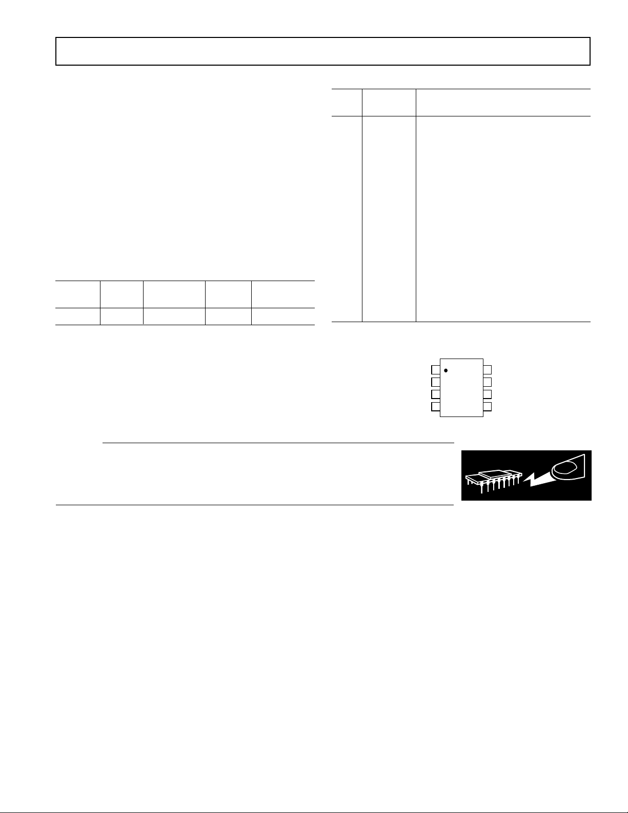
PIN FUNCTION DESCRIPTIONS
Pin
No. Mnemonic Function
1, 2, 3 OUT Output of the Regulator. Bypass to
ground with a 1.0 µF or larger capacitor.
All pins must be connected together for
proper operation.
4 GND Ground Pin.
5 FB Feedback Input. Connect to an external
resistor divider which sets the output
voltage. Can also be used for further
reduction of output noise (see text for
detail).
Capacitor required if C
> 3.3 µF.
OUT
6 SD Active Low Shutdown Pin. Connect to
ground to disable the regulator output.
When shutdown is not used, this pin
should be connected to the input pin.
7, 8 IN Regulator Input. All pins must be con-
nected together for proper operation.
PIN CONFIGURATION
OUT
OUT
OUT
GND
1
2
ADP3336
TOP VIEW
3
(Not to Scale)
4
8
IN
7
IN
6
SD
5
FB
CAUTION
ESD (electrostatic discharge) sensitive device. Electrostatic charges as high as 4000 V readily
accumulate on the human body and test equipment and can discharge without detection. Although
the ADP3336 features proprietary ESD protection circuitry, permanent damage may occur on
devices subjected to high-energy electrostatic discharges. Therefore, proper ESD precautions are
recommended to avoid performance degradation or loss of functionality.
WARNING!
ESD SENSITIVE DEVICE
REV. 0
–3–
 Loading...