a
Adjustable Output Ultralow IQ, 200 mA,
®
SOT-23, anyCAP
Low Dropout Regulator
ADP3331
FEATURES
High Accuracy over Line and Load: ⴞ0.7% @ 25ⴗC,
1.4% over Temperature
Ultralow Dropout Voltage: 140 mV (Typ) @ 200 mA
Can Be Used as a High Current (>1 A) LDO
Controller
Requires Only C
= 0.47 F for Stability
O
anyCAP = Stable with Any Type of Capacitor
(Including MLCC)
Current and Thermal Limiting
Low Noise
Low Shutdown Current: 10 nA Typical
2.6 V to 12 V Supply Range
1.5 V to 11.75 V Output Range
–40ⴗC to +85ⴗC Ambient Temperature Range
Ultrasmall Thermally Enhanced Chip-on-Lead™
SOT-23-6 Lead Package
APPLICATIONS
Cellular Telephones
Notebook, Palmtop Computers
Battery-Powered Systems
PCMCIA Regulators
Bar Code Scanners
Camcorders, Cameras
ERR
SD
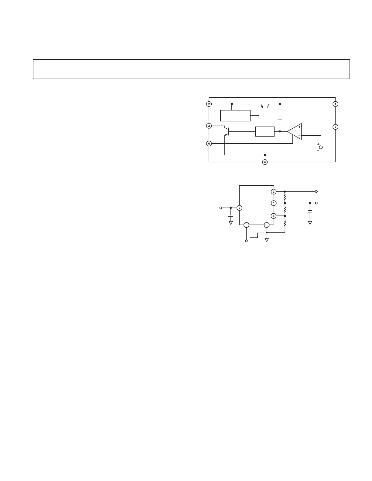
FUNCTIONAL BLOCK DIAGRAM
IN
THERMAL
PROTECTION
Q2
V
IN
0.47F
C1
IN
+
Q1
CC
DRIVER
GND
ERR
ADP3331
OUT
OFF
ON
GND
FB
SD
64
R3
330k⍀
R1
R2
ADP3331
g
m
BAND GAP
+
REF
E
V
C2
0.47F
OUT
OUT
OUT
FB
Figure 1. Typical Application Circuit
GENERAL DESCRIPTION
The ADP3331 is a member of the ADP330x family of precision
low dropout anyCAP voltage regulators. The ADP3331 operates
with an input voltage range of 2.6 V to 12 V and delivers a load
current up to 200 mA. The ADP3331 stands out from the
conventional LDOs with a novel architecture and an enhanced
process that enables it to offer performance advantages and higher
output current than its competition. Its patented design requires
only a 0.47 mF output capacitor for stability. This device is insensi-
tive to capacitor equivalent series resistance (ESR), and is stable
with any good quality capacitor, including ceramic (MLCC) types
REV. A
Information furnished by Analog Devices is believed to be accurate and
reliable. However, no responsibility is assumed by Analog Devices for its
use, nor for any infringements of patents or other rights of third parties that
may result from its use. No license is granted by implication or otherwise
under any patent or patent rights of Analog Devices. Trademarks and
registered trademarks are the property of their respective companies.
for space restricted applications. The ADP3331 achieves exceptional accuracy of ± 0.7% at room temperature and ±1.4% overall
accuracy over temperature, line, and load variations. The dropout voltage of the ADP3331 is only 140 mV (typical) at 200 mA.
This device also includes a safety current limit, thermal overload protection, and a shutdown feature. In shutdown mode, the
ground current is reduced to less than 2 mA. The ADP3331 has
ultralow quiescent current 34 mA (typical) in light load situations.
The SOT-23-6 package has been thermally enhanced using
Analog Device’s proprietary Chip-on-Lead feature to maximize power dissipation.
One Technology Way, P.O. Box 9106, Norwood, MA 02062-9106, U.S.A.
Tel: 781/329-4700 www.analog.com
Fax: 781/326-8703 © 2003 Analog Devices, Inc. All rights reserved.

ADP3331–SPECIFICATIONS
(TA = –40ⴗC to +85ⴗC, VIN = 7 V, CIN = 0.47 F, C
1, 2
noted.)
= 0.47 F, unless otherwise
OUT
Parameter Symbol Conditions Min Typ Max Unit
OUTPUT VOLTAGE ACCURACY
HIGH OUTPUT VOLTAGE RANGE V
3
VIN = V
I
T
V
V
OUTNOM
OUTNOM
= 0.1 mA to 200 mA,
L
= 25∞C –0.7 +0.7 %
A
= V
IN
OUTNOM
OUTNOM
+ 0.25 V to 12 V,
≥ 2.35 V,
+ 0.25 V to 12 V,
≥ 2.35 V,
IL = 0.1 mA to 150 mA,
= –40∞C to +85∞C –1.4 +1.4 %
T
A
= V
V
IN
V
I
OUTNOM
OUTNOM
= 0.1 mA to 200 mA,
L
+ 0.25 V to 12 V,
≥ 2.35 V,
TA = –20∞C to +85∞C –1.4 +1.4 %
OUTPUT VOLTAGE ACCURACY
LOW OUTPUT VOLTAGE RANGE V
3
VIN = 2.6 V to 12 V,
OUTNOM
I
L
T
A
V
IN
V
OUTNOM
I
L
T
A
V
IN
V
OUTNOM
I
L
= 1.5 V to 2.35 V,
= 0.1 mA to 200 mA,
= 25∞C –0.7 +0.7 %
= 2.6 V to 12 V,
= 1.5 V to 2.35 V,
= 0.1 mA to 150 mA,
= –40∞C to +85∞C –1.4 +1.4 %
= 2.6 V to 12 V,
= 1.5 V to 2.35 V,
= 0.1 mA to 200 mA,
TA = –20∞C to +85∞C –1.4 +1.4 %
LINE REGULATION DV
DV
LOAD REGULATION DV
DI
GROUND CURRENT I
GND
O
IN
O
L
VIN = V
OUTNOM
TA = 25∞C 0.06 mV/V
IL= 0.1 mA to 200 mA
TA = 25∞C 0.04 mV/mA
IL = 200 mA, TA = –20∞C to +85∞C 1.6 4.0 mA
= 150 mA 1.2 3.1 mA
I
L
= 50 mA 0.4 1.1 mA
I
L
+ 0.25 V to 12 V
IL = 0.1 mA 34 50 mA
GROUND CURRENT I
GND
VIN = V
OUTNOM
– 100 mV
IN DROPOUT IL = 0.1 mA 37 55 mA
DROPOUT VOLTAGE
2
V
DROP
V
= 98% of V
OUT
OUTNOM
IL = 200 mA, TA = –20∞C to +85∞C 0.14 0.23 V
I
= 150 mA 0.11 0.17 V
L
= 10 mA 0.042 0.06 V
I
L
IL = 1 mA 0.025 0.05 V
PEAK LOAD CURRENT I
OUTPUT NOISE V
SHUTDOWN THRESHOLD V
LDPK
NOISE
THSD
VIN = V
OUTNOM
+ 1 V 300 mA
f = 10 Hz–100 kHz, CL = 10 mF
I
= 200 mA, CNR = 10 nF, V
L
f = 10 Hz–100 kHz, C
= 10 mF
L
IL = 200 mA, CNR = 0 nF, V
= 3 V 47 mV rms
OUT
= 3 V 95 mV rms
OUT
ON 2.0 V
OFF 0.4 V
SHUTDOWN PIN INPUT CURRENT I
SD
0 < SD £ 12 V 1.9 9 mA
0 < SD £ 5 V 1.4 6 mA
GROUND CURRENT IN
SHUTDOWN MODE I
GNDSD
SD = 0 V, VIN = 12 V 0.01 2 mA
–2–
REV. A

ADP3331
Parameter Symbol Conditions Min Typ Max Unit
OUTPUT CURRENT IN I
OSD
SHUTDOWN MODE TA = 85∞C @ VIN = 12 V 2 mA
ERROR PIN OUTPUT LEAKAGE I
EL
ERROR PIN OUTPUT
LOW VOLTAGE V
NOTES
1
Ambient temperature of 85∞C corresponds to a junction temperature of 125 ∞C under typical full load test conditions.
2
Application stable with no load.
3
Assumes the use of ideal resistors. Overall accuracy also depends on the tolerance of the external resistors used to set the output voltage.
Specifications subject to change without notice.
EOL
TA = 25∞C @ VIN = 12 V 1 mA
VEO = 5 V 1 mA
I
= 400 mA 0.19 0.40 V
SINK
ABSOLUTE MAXIMUM RATINGS*
Input Supply Voltage . . . . . . . . . . . . . . . . . . . .–0.3 V to +16 V
Shutdown Input Voltage . . . . . . . . . . . . . . . . . –0.3 V to +16 V
Power Dissipation . . . . . . . . . . . . . . . . . . . . Internally Limited
Operating Ambient Temperature Range . . . . –40∞C to +85∞C
Operating Junction Temperature Range . . . –40∞C to +125∞C
(4-Layer Board) . . . . . . . . . . . . . . . . . . . . . . . . 165∞C/W
q
JA
q
(2-Layer Board) . . . . . . . . . . . . . . . . . . . . . . . . 190∞C/W
JA
Storage Temperature Range . . . . . . . . . . . . –65∞C to +150∞C
Lead Temperature Range (Soldering 10 sec) . . . . . . . . . 300∞C
Vapor Phase (60 sec) . . . . . . . . . . . . . . . . . . . . . . . . . 215∞C
Infrared (15 sec) . . . . . . . . . . . . . . . . . . . . . . . . . . . . . 220∞C
*Stresses above those listed under Absolute Maximum Ratings may cause perma-
nent damage to the device. This is a stress rating only; functional operation of the
device at these or any other conditions above those listed in the operational
sections of this specification is not implied. Exposure to absolute maximum rating
conditions for extended periods may affect device reliability.
ORDERING GUIDE
Output
Model Voltage Package Option Branding
ADP3331ART ADJ RT-6 (SOT-23-6) L9B
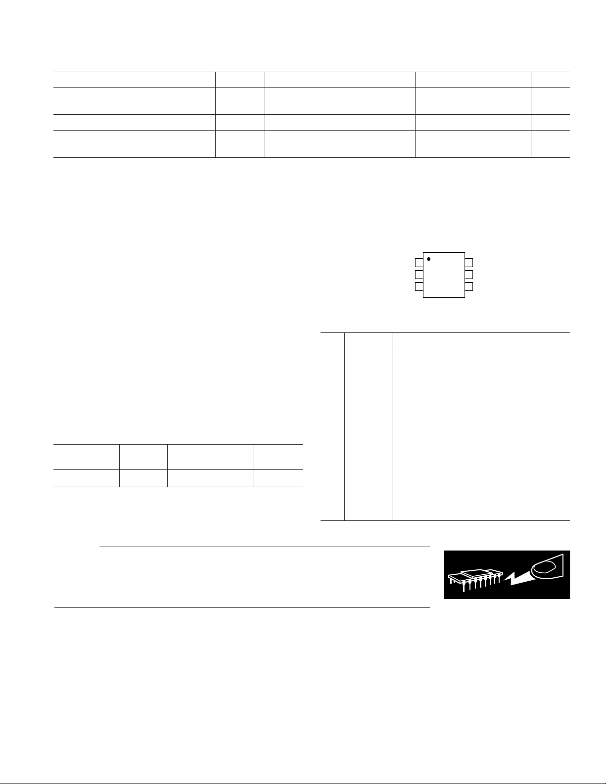
PIN CONFIGURATION
OUT
ERR
1
2
IN
3
ADP3331
TOP VIEW
(Not to Scale)
6
SD
5
FB
4
GND
PIN FUNCTION DESCRIPTIONS
Pin Name Function
1 OUT Output of the Regulator. Bypass to ground
with a 0.47 mF or larger capacitor.
2INRegulator Input.
3 ERR Open Collector Output that goes low to
indicate that the output is about to go out
of regulation.
4GND Ground.
5FBFeedback Input. Connect to an external
resistor divider, which sets the output
voltage.
6 SD Active Low Shutdown Pin. Connect to
ground to disable the regulator output.
When shutdown is not used, this pin
should be connected to the input pin.
CAUTION
ESD (electrostatic discharge) sensitive device. Electrostatic charges as high as 4000 V readily
accumulate on the human body and test equipment and can discharge without detection.
Although the ADP3331 features proprietary ESD protection circuitry, permanent damage may
occur on devices subjected to high energy electrostatic discharges. Therefore, proper ESD
precautions are recommended to avoid performance degradation or loss of functionality.
REV. A
–3–
WARNING!
ESD SENSITIVE DEVICE

ADP3331
)
)
)
)
)
)
)
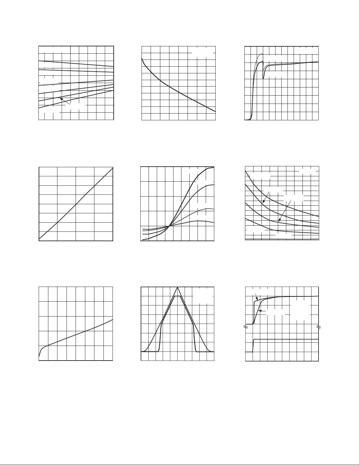
–Typical Performance Characteristics
3.010
V
= 3.0V
OUT
3.008
3.006
IL = 0mA
3.004
IL = 10mA
3.002
IL = 50mA
3.000
IL = 100mA
2.998
2.996
OUTPUT VOLTAGE (V)
2.994
IL = 200mA
2.992
2.990
3.25
4567 89101112
= 150mA
I
L
INPUT VOLTAGE (V
TPC 1. Line Regulation Output
Voltage vs. Supply Voltage
1.6
VIN = 7V
1.4
1.2
1.0
0.8
0.6
0.4
GROUND CURRENT (mA)
0.2
0
0
50 200
100 150
OUTPUT LOAD (mA
TPC 4. Ground Current vs. Load
Current
3.005
3.004
3.003
3.002
3.001
3.000
2.999
2.998
2.997
OUTPUT VOLTAGE (V)
2.996
2.995
2.994
25
50 75 100 125 150 175 200
0
OUTPUT LOAD (mA
V
= 3.0V
OUT
= 7V
V
IN
TPC 2. Output Voltage vs. Load
Current
0.4
0.3
0.2
0.1
OUTPUT VOLTAGE (%)
0.0
–0.1
–45 –25 135–5 15 35 75 95 11555
JUNCTION TEMPERATURE (ⴗC)
IL = 0mA
IL = 50mA
IL = 150mA
IL = 200mA
TPC 5. Output Voltage Variation % vs.
Junction Temperature
45
40
35
30
25
20
15
GROUND CURRENT (A)
10
5
0
0
IL = 100A
IL = 0A
246 810 12
INPUT VOLTAGE (V
V
= 3V
OUT
TPC 3. Ground Current vs. Supply
Voltage
3.0
2.8
IL = 200mA
2.6
2.4
2.2
2.0
1.8
1.6
1.4
1.2
1.0
0.8
GROUND CURRENT (mA)
0.6
0.4
0.2
0
–45 –25 115
IL = 150mA
IL = 50mA
IL = 0mA
–5 15 35 55 75 95
JUNCTION TEMPERATURE (ⴗC)
VIN = 7V
IL = 100mA
TPC 6. Ground Current vs. Junction
Temperature
135
250
200
150
100
50
INPUT/OUTPUT VOLTAGE (mV)
0
025 10050 75
OUTPUT LOAD (mA
125 150 175 200
TPC 7. Dropout Voltage vs.
Output Current
3.5
3.0
2.5
2.0
1.5
1.0
0.5
INPUT/OUTPUT VOLTAGE (V)
0
0 1.0 2.0 3.0 4.0 5.0
TIME (sec
V
OUT
SD = V
RL = 15⍀
TPC 8. Power-Up/Power-Down
–4–
= 3V
IN
CL = 0.47F
3
(V)V
2
OUT
V
1
0
10
(V)
5
IN
0
0 100 200 300 400 500
CL = 10F
TIME (s
VIN = 7V
= 3V
V
OUT
SD = V
RL = 15⍀
IN
TPC 9. Power-Up Response
REV. A
 Loading...