

Precision Voltage
GND
V
OUT
GATE
EN
V
IN
50mV
V
REF
IS
ADP3310
+
–
BIAS
NDP6020P
V
OUT
10mF
V
IN
1mF
IS
GATE
GND
EN
V
IN
V
OUT
ADP3310
+
–
+
–
R
S
50mV
ON
OFF
a
FEATURES ⴞ1.5% Accuracy Over Line, Load and Temperature Low 800 A (Typical) Quiescent Current Shutdown Current: 1 A (Typical) Stable with 10 F Load Capacitor +2.5 V to +15 V Operating Range Fixed Output Voltage Options: 2.8 V, 3 V, 3.3 V, 5 V Up to 10 A Output Current SO-8 Package –40ⴗC to +85ⴗC Ambient Temperature Range Internal Gate to Source Protective Clamp Current and Thermal Limiting Programmable Current Limit Foldback Current Limit
APPLICATIONS
Desktop Computers
Handheld Instruments
Cellular Telephones
Battery Operated Devices
Solar Powered Instruments
High Efficiency Linear Power Supplies
Battery Chargers
Regulator Controller
ADP3310
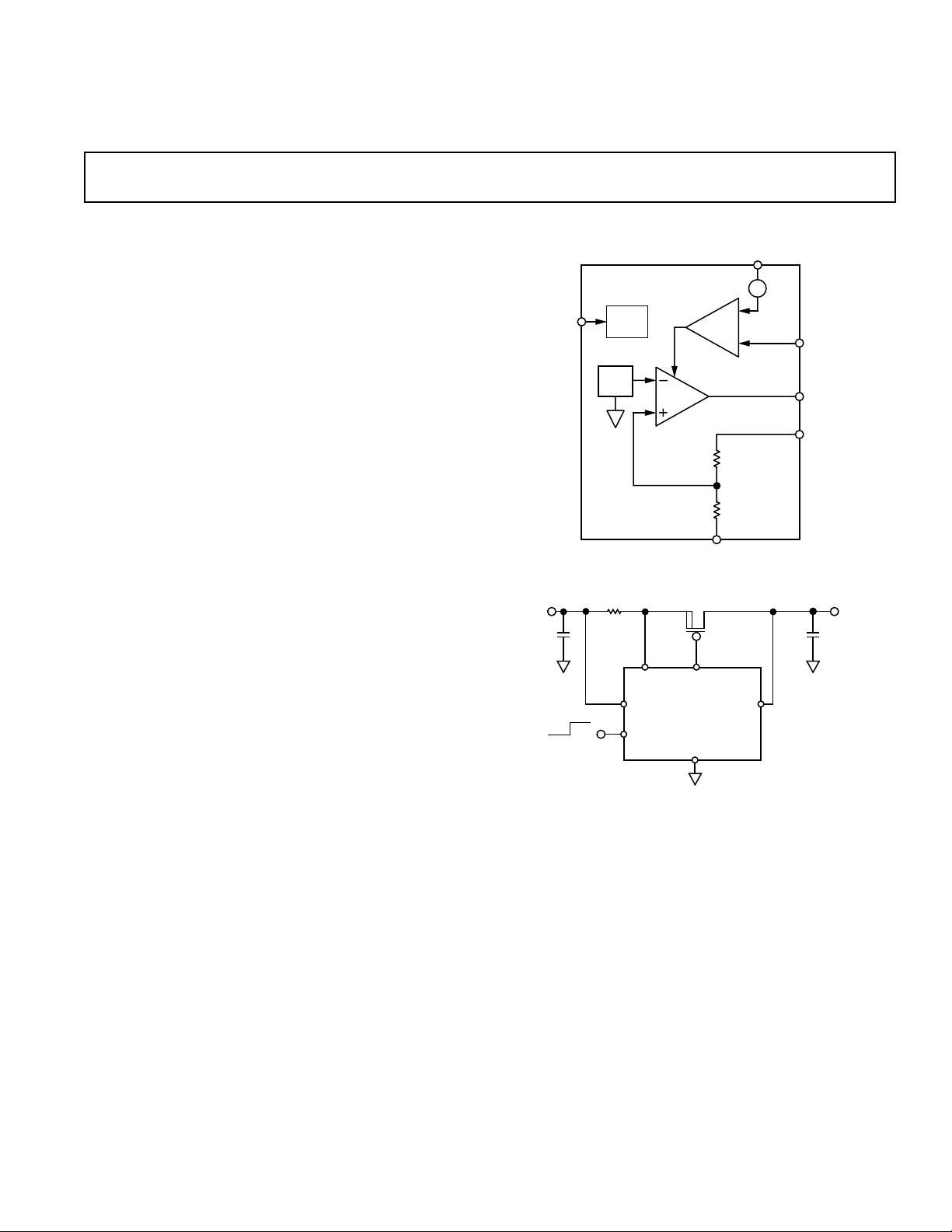
FUNCTIONAL BLOCK DIAGRAM
GENERAL DESCRIPTION
The ADP3310 is a precision voltage regulator controller that
can be used with an external Power PMOS device such as the
NDP6020P to form a two chip low dropout linear regulator.
The low quiescent current (800 µA) and the Enable feature
make this device especially suitable for battery powered systems.
The dropout voltage at 1 A is only 70 mV when used with the
NDP6020P, allowing operation with minimal headroom and
prolonging battery useful life. The ADP3310 can drive a wide
range of currents, depending on the external PMOS device used.
Additional features of this device include: high accuracy (±1.5%)
over line, load and temperature, gate-to-source voltage clamp to
protect the external MOSFET and foldback current limit. A
current limit threshold voltage of 50 mV (typ) allows 50 mΩ of
board metal trace resistance to provide a 1 A current limit.
The ADP3310 operates from a wide input voltage range from
2.5 V to 15 V and is available in a small SO-8 package.
REV. A
Information furnished by Analog Devices is believed to be accurate and
reliable. However, no responsibility is assumed by Analog Devices for its
use, nor for any infringements of patents or other rights of third parties
which may result from its use. No license is granted by implication or
otherwise under any patent or patent rights of Analog Devices.
Figure 1. Typical Application Circuit
One Technology Way, P.O. Box 9106, Norwood, MA 02062-9106, U.S.A.
Tel: 781/329-4700 World Wide Web Site: http://www.analog.com
Fax: 781/326-8703 © Analog Devices, Inc., 1999
ADP3310–SPECIFICATIONS
(VIN = V
+ 1 V, TA = –40ⴗC to +85ⴗC unless otherwise noted)
OUT
Parameter Conditions Symbol Min Typ Max Units
OUTPUT VOLTAGE ACCURACY (Figure 1) V
= V
IN
V
EN
to 1 A V
OUT
= 2 V, I
+1 V to 15 V
= 10 mA
OUT
OUT
–1.5 +1.5 %
QUIESCENT CURRENT
Shutdown Mode V
= 0 V I
EN
Normal Mode VEN = 2 V, I
GATE TO SOURCE CLAMP VOLTAGE V
= 0 V, VIN = 15 V 8 10 V
OUT
= 500 µAI
OUT
GND
GND
110µA
800 1000 µA
GATE DRIVE MINIMUM VOLTAGE 0.7 V
GATE DRIVE CURRENT (SINK/SOURCE) 1 mA
GAIN
CURRENT LIMIT THRESHOLD VOLTAGE VIN – V
LOAD REGULATION I
LINE REGULATION V
SHUTDOWN INPUT VOLTAGE V
SHUTDOWN INPUT CURRENT VEN = 0 V to 5.0 V I
Specifications subject to change without notice.
∆V
∆V
GS
OUT
IS
= 10 mA to 1 A –10 10 mV
OUT
I
OUT
V
IN
IH
IL
= V
+1 V to 15 V
OUT
= 100 mA –10 10 mV
V
EN
EN
40 50 80 mV
2.0 V
–10 +10 µA
80 dB
0.4 V
ABSOLUTE MAXIMUM RATINGS*
Input Voltage, VIN␣ . . . . . . . . . . . . . . . . . . . . . . . . . . . +20 V
Enable Input Voltage . . . . . . . . . . . . . . . 0.3 V to V
+ 0.3 V
IN
Operating Junction Temperature Range . . . –40°C to +125°C
Operating Temperature Range . . . . . . . . . . . –40°C to +85°C
Storage Temperature Range . . . . . . . . . . . . –65°C to +150°C
Lead Temperature (Soldering, 10 sec) . . . . . . . . . . . +300°C
Vapor Phase (60 sec) . . . . . . . . . . . . . . . . . . . . . . . . . +215°C
Infrared (15 sec) . . . . . . . . . . . . . . . . . . . . . . . . . . . . +220°C
(4-Layer Board) . . . . . . . . . . . . . . . . . . . . . . . . +121°C/W
θ
JA
(2-Layer Board . . . . . . . . . . . . . . . . . . . . . . . . . +150°C/W
θ
JA
*This is a stress rating only; operation beyond these limits can cause the device to
be permanently damaged.
CAUTION
ESD (electrostatic discharge) sensitive device. Electrostatic charges as high as 4000 V readily
accumulate on the human body and test equipment and can discharge without detection. Although
the ADP3310 features proprietary ESD protection circuitry, permanent damage may occur on
devices subjected to high energy electrostatic discharges. Therefore, proper ESD precautions are
recommended to avoid performance degradation or loss of functionality.
WARNING!
ESD SENSITIVE DEVICE
–2–
REV. A
ADP3310
1
2
3
4
8
7
6
5
TOP VIEW
(Not to Scale)
NC = NO CONNECT
ADP3310
IS
NC
GND
EN
NC
GATE
V
IN
V
OUT
ORDERING GUIDE
Model Output Voltage Package Option*
ADP3310AR-2.8 2.8 V SO-8
ADP3310AR-3 3 V SO-8
ADP3310AR-3.3 3.3 V SO-8
ADP3310AR-5 5 V SO-8
*SO = Small Outline. Contact the factory for the availability of other output
voltage options from 5 V to 16.5 V.
Refer to the ADP3319 data sheet for 1.8 V and 2.5 V output voltage options.
Refer to the ADP3328 data sheet for adjustable output version.
PIN FUNCTION DESCRIPTIONS
Pin
SO-8 Name Function
1 IS Current Sense. Connected to the more
negative terminal of the sense resistor as
well as the Power MOSFET’s source pin.
IS must be tied to V
pin if the current
IN
limit feature is not used.
2, 6 NC No Connect.
3 GATE Gate Drive for the external MOSFET.
4V
IN
Input Voltage. This is also the positive
terminal connection of the current sense
resistor.
5V
OUT
Output Voltage Sense. This pin is
connected to the MOSFET’s drain and
directly to the load for optimal load regula-
tion. Bypass to ground with a 10 µF or
larger capacitor.
7 GND Device Ground. This pin should be tied to
system ground closest to the load.
8 EN Enable. Pulling this pin to a logic High or
tying the pin to the input voltage will enable
the output. Pulling this pin low will disable
the regulator output.
PIN CONFIGURATION
SO-8
REV. A
Table I. Alternate PMOS Devices
PMOS NDP6020P IRF7404 Si9434DY
Manufacturer Fairchild IR Temic
R
DS(ON)
Continuous @ 25°C –27 A @ V
I
D
@ 25°C 75 W 1.6 W 2.5 W
P
D
0.075 Ω @ VGS = –2.5 V 0.06 Ω @ VGS = –2.7 V 0.06 Ω @ V
= –4.5 V –5.3 A @ VGS = –4.5 V –6.4 A
GS
Derating Factor 0.5 W/°C 0.011 W/°C 1.6 W @ 70°C
Package TO-220 SO-8 SO-8
–3–
= –2.5 V
GS

ADP3310
VIN – V
I
GND
– mA
1.6
0
1.4
0.8
0.6
0.4
0.2
1.2
1.0
3.5 5.5 15.57.5 9.5 11.5 13.5
I
LOAD
= 10mA
VIN – V
I
GND
– mA
2.0
0
3.5 5.5 15.5
7.5 9.5 11.5 13.5
1.8
0.8
0.6
0.4
0.2
1.6
1.4
1.0
1.2
I
LOAD
= 1A
I
LOAD
– mA
I
GND
– mA
1.2
0.5
0.001 0.01 10000.1 1 10 100
1.1
1.0
0.9
0.7
0.6
0.8
VIN = 5V
3.310
3.305
– V
3.300
OUT
V
3.295
3.290
0.001 0.01 10000.1 0 10 100
3.310
3.305
– V
3.300
OUT
V
–Typical Performance Characteristics (Circuit of Figure 1)
VIN = 5V
I
– mA
LOAD
Figure 2. V
I
= 1A
LOAD
OUT
vs. I
(VIN = 5 V)
LOAD
Figure 5. I
vs. VIN (I
GND
= 10 mA)
LOAD
3.295
3.290
3.5 5.5 15.5
Figure 3. V
3.310
I
LOAD
3.305
– V
3.300
OUT
V
3.295
3.290
3.7 4 15
Figure 4. V
7.5 9.5 11.5 13.5
VIN – V
vs. VIN (I
OUT
= 10mA
4.5 5 7 9 11 13
OUT
VIN – V
vs. VIN (I
LOAD
= 10 mA)
LOAD
= 1 A)
–4–
Figure 6. I
Figure 7. I
vs. VIN (I
GND
vs. I
GND
LOAD
(VIN = 5 V)
LOAD
= 1 A)
REV. A

1.5
I
LOAD
3.200
3.400
3.300
1A
10mA
250 ms/DIV
V
OUT
– V
VIN = 5V
C
L
= 10mF
FREQUENCY – Hz
0
–80
110 1M100 1k 10k 100k
–10
–20
–30
–50
–60
–40
–70
PSRR – dB
C
LOAD
= 10mF
I
LOAD
= 1mA
VIN = 5V
1.4
1.3
1.2
1.1
1.0
– mA
GND
I
0.9
0.8
0.7
0.6
0.5
–40 –20 800204060
I
LOAD
= 10mA
TEMPERATURE – 8C
Figure 8. Quiescent Current vs. Temperature
3.5
I
= 10mA
LOAD
3.0
2.5
2.0
– V
OUT
1.5
V
ADP3310
Figure 11. Load Transient Response
1.0
0.5
0
2.0 2.8 5.0 2.8 2.0
00
Figure 9. Power-Up/Power-Down
I
= 10mA
LOAD
= 10mF
C
L
7.0
– V
IN
V
5.5
3.32
– V
3.30
OUT
V
3.28
Figure 10. Line Transient Response—(10 µF Load)
REV. A
VIN – V
5ms/DIV
–5–
Figure 12. Ripple Rejection
4.0
VIN = 5V
RCS = 0.50
3.5
3.0
2.5
– V
2.0
OUT
V
1.5
1.0
0.5
0
0 20 180
40 60 80 120 140 160100
I
LOAD
– mA
Figure 13. Foldback Current

ADP3310
APPLICATION INFORMATION
The ADP3310 is very easy to use. A P-channel power MOSFET
and a small capacitor on the output is all that is needed to form
an inexpensive ultralow dropout regulator. The advantage of
using the ADP3310 controller is that it can drive a pass PMOS
FET to provide a regulated output at high current.
FET Selection
The type and size of the pass transistor are determined by the
threshold voltage, input-output voltage differential and load
current. The selected PMOS must satisfy the physical and
thermal design requirements. Table I shows a partial list of
manufacturers providing the PMOS devices. To ensure that the
maximum V
provided by the controller will turn on the FET
GS
at worst case conditions (i.e., temperature and manufacturing
tolerances), the maximum available V
Maximum V
(1) V
GS
I
OMAX
R
S
V
BE
is calculated as follows:
GS
= VIN – VBE – I
OMAX
× R
= Maximum Output Current
= Current Sense Resistor
~ 0.7 V (Room Temp)
must be determined.
GS
S
~ 0.5 V (Hot)
~ 0.9 V (Cold)
For Example: V
= 5 V – 0.7 V – 3 A × 11 mΩ = 4.27 V
V
GS
= 5 V, VO = 3.3 V and I
IN
OMAX
= 3 A,
Equation (1) applies to a gate-to-source voltage less than the
gate to source clamp voltage.
(2) V
= VIN – V
DS
O
VDS = 5 V – 3.3 V = 1.7 V
If V
≤ 5 V, logic level FET should be considered.
IN
> 5 V, either logic level or standard MOSFET can be used.
If V
IN
The difference between V
and V
IS
(VDS) must exceed the
OUT
voltage drop due to the load current and the ON resistance of
the FET. As a safety margin, it is recommended to use a MOSFET with a V
at least 1.5 times lower than the calculated V
GS
GS
value from Equation 1. Also, in the event the circuit is shorted
to ground, the MOSFET must be able to conduct the maximum
short circuit current. The selected MOSFET must satisfy these
criteria; otherwise, a different pass device should be used. If the
FET data is not available in the catalogue, contact the FET
manufacturer.
Thermal Design
The maximum allowable thermal resistance between the FET
junction and the highest ambient temperature must be taken
into account to determine the type of FET package used. One
square inch of PCB copper area as heatsink yields a typical
~ 60°C/W for the SOT-223 package and θJA ~ 50°C/W for
θ
JA
the SO-8 package. For substantially lower thermal resistances,
2
PAK or TO-220 type of packages are recommended.
D
For normal applications, the FET can be directly mounted to the
PCB. But, for higher power applications, an external heat sink is
required to satisfy the θ
Calculating thermal resistance for V
= 3 A:
I
O
T
J
T
AMBMAX
= Junction Temperature
= Maximum Ambient Temperature
requirement and provide adequate heatsink.
JA
= 5 V, VO = 3.3 V, and
IN
T
– T
J
θJA=
(V
DSMAX
AMBMAX
× I
OMAX
)
V
DSMAX
I
OMAX
θ
JA
For such a low θ
= Maximum Drain to Source Voltage
= Maximum Output Current
125 −50
=
1. 7 ×3
=14.7°C/W
, a P-channel FET from Fairchild, such as
JA
NDP6020P in a heatsink mountable TO-220 package, is
required. The required external heatsink is determined as
follows:
θ
= θ
CA
θ
CA
θ
JA
θ
JC
θ
JC
θ
CA
For a safety margin, select a heatsink with a θ
– θ
JA
JC
= Case-to-Ambient Thermal Resistance
= Junction-to-Ambient Thermal Resistance
= Junction-to-Case Thermal Resistance
= 2°C/W for NDP6020P
= 14.7°C/W – 2°C/W = 12.7°C/W
CA
less than half of
the value calculated above to allow extended duration of short
circuit. In a natural convection environment, a large heatsink
such as 3" length of Type 63020 extrusion from Aavid Engineering
is required.
External Capacitors
The ADP3310 is stable with virtually any good quality capacitors (anyCAP™), independent of the capacitor’s minimum ESR
(Effective Series Resistance) value. The actual value of the capacitor and its associated ESR depends on the g
and ca-
m
pacitance of the external PMOS device. A 10 µF capacitor at the
output is sufficient to ensure stability for up to 10 A output
current. Larger capacitors can be used if high output current
surges are anticipated. Extremely low ESR capacitors (ESR≈0)
such as multilayer ceramic or OSCON are preferred because
they offer lower ripple on the output. For less demanding
requirements, a standard tantalum or even an aluminum
electrolytic is adequate. However, if an aluminum electrolytic is
used, be sure it meets the temperature requirements because
aluminum electrolytic has poor performance over temperature.
Shutdown Mode
Applying a TTL high signal to the EN pin or tying it to the
input pin will enable the output. Pulling this pin low or tying it
to ground will disable the output. In shutdown mode, the
controller’s quiescent current is reduced to less than 1 µA.
Gate-to-Source Clamp
An 8 V gate-to-source voltage clamp is provided to protect the
MOSFET in the event the output is suddenly shorted to
ground. This allows the use of the new, low on-state resistance
) FETs.
(R
DSON
Short Circuit Protection
The power FET is protected during short circuit conditions
with a foldback type of current limiting which significantly reduces the current.
Current Sense Resistor
Current limit is achieved by setting an appropriate current sense
resistor (R
limit sense resistor R
anyCAP is a trademark of Analog Devices, Inc.
) across the current limit threshold voltage. Current
S
is calculated as follows:
S
0.05
R
=
S
(1.5 ×I
)
O
–6–
REV. A

ADP3310
M1
NDP6020P
10mF
4.5V TO 5.5V
10mF
IS
GND
EN
V
IN
V
OUT
ADP3310-3.3
+
R2
0.011V
GATE
1kV
220mF
OSCON
+
3 3 220mF
OSCON
3.3V
Current Limit Threshold Voltage = 0.05 V
Safety Factor = 1.5
= Output Current
I
O
R
is not needed in circuits that do not require current limiting.
S
In that case, the I
pin must be tied to the input pin.
S
The simplest and cheapest sense resistor for high current applications, (i.e., Figure 1) is a PCB trace. The temperature dependence of the copper trace and the thickness tolerances of the
trace must be taken into account in the design. The resistivity of
copper has a positive temperature coefficient of +0.39%/°C.
Copper’s Tempco in conjunction with the proportional-toabsolute temperature (PTAT) current limit voltage can provide
an accurate current limit. Table II provides the resistance value
for PCB copper traces. Alternately, an appropriate sense resistor
such as surface mount sense resistors available from KRL can be
used.
PCB-Layout Issues
For optimum voltage regulation, place the load as close as possible to the device’s V
and GND pins. It is recommended to
OUT
use dedicated PCB traces to connect the MOSFET’s drain to
the positive terminal and GND to the negative terminal of the
load to avoid voltage drops along the high current carrying PCB
traces.
Application Circuits
Typical 3 A LDO Circuit
The ADP3310 and a power MOSFET can be used to power the
new generation of CPUs and microprocessors from the standard
+5 V supply at a very low cost (Figure 14). This circuit provides
low dropout, fast switching and high switching load current
from 0 A to 3 A. Due to the high switching load current, capacitors with high ripple current carrying capability, such as OSCON
or special tantalum capacitors from Sprague (593D), are recommended for the output.
Table II. Printed Circuit Copper Resistance
Conductor Conductor Width Resistance
Thickness In mΩ/In
1/2 oz/ft
2
0.025 39.3
(18 µm) 0.050 19.7
0.100 9.83
0.200 4.91
0.500 1.97
2
1 oz/ft
0.025 19.7
(35 µm) 0.050 9.83
µ
0.100 4.91
50mV/div 2V/div
s/div
5
0.200 2.46
0.500 0.98
2
2 oz/ft
0.025 9.83
(70 µm) 0.050 4.91
0.100 2.46
0.200 1.23
0.500 0.49
2
3 oz/ft
0.025 6.5
(106 µm) 0.050 3.25
0.100 1.63
0.200 0.81
0.500 0.325
REV. A
R
C
1kV
C
C
22nF
470pF
OSCON
220mF
C
T
C2
10nF
Figure 14. Typical 3 A Low Dropout Regulator Circuit
= 5V TO 15V
V
IN
+
C
IN
V
IN
P-DRIVE
INT V
CC
SD
ADP1148
SENSE
I
SENSE
TH
C
N-DRIVE
T
S-GND P-GND
C1
1mF
+
–
FB
** COILTRONICS CTX-68-4
** KRL SL-1-C1-ORO5OL
IRF7204
L*
68µH
C3
1nF
N-CH
IRF7403
R
SENSE
0.1V
D1
10BQ040
**
OSCON
220mF
C4
2N3906
Q1
R1
30.1kV
1%
R2
124kV
1%
Figure 15. High Current Post Regulator with SOIC PMOS
–7–
MI
IRF7404
GATE
IS
IN OUT
ADP3310-3.3
EN
GND
2N3906
3.3V/1A
C5
BAT54
Q2
R3
274kV
10mF

ADP3310
V
OS
20mV/div
10mV/div
V
O
5ms
High Current Post Regulator with SOIC PMOS
Post regulation for a switch-mode supply (Figure 15) can be
implemented with a PMOS in an SO-8 package to provide a
significant reduction in peak-to-peak ripple voltage. A constant
dropout voltage in conjunction with low quiescent current yield
a more efficient voltage regulator that can significantly extend
battery life. The bottom waveform of Figure 16 is the output of
the switching regulator. The top waveform is the output of the
post regulator.
In applications where cost is a higher concern than efficiency, a
resistor divider can be used to provide feedback instead of the
current mirror. Power efficiency is lower in cases of light loads.
0.1574 (4.00)
0.1497 (3.80)
PIN 1
0.0098 (0.25)
0.0040 (0.10)
SEATING
Figure 16. Pre-and Post-Regulated Voltage
OUTLINE DIMENSIONS
Dimensions shown in inches and (mm).
8-Lead Small Outline
(SO-8)
0.1 968 (5.00)
0.1 890 (4.80)
85
0.0500 (1.27)
PLANE
0.2440 (6.20)
0.2284 (5.80)
41
BSC
0.0192 (0.49)
0.0138 (0.35)
0.0688 (1.75)
0.0532 (1.35)
0.0098 (0.25)
0.0075 (0.19)
0.0196 (0.50)
0.0099 (0.25)
88
0.0500 (1.27)
08
0.0160 (0.41)
3 458
5mAOS
5M
55mV
C2982a–0–12/99 (rev. A)
PRINTED IN U.S.A.
–8–
REV. A
 Loading...