ANALOG DEVICES ADP3309 Service Manual

anyCAP® 100 mA
C
www.BDTIC.com/ADI
FEATURES
±1.2% accuracy over line and load regulations @ 25°C
Ultralow dropout voltage: 120 mV typical @ 100 mA
Requires only C
anyCAP LDOs are stable with all types of capacitors
(including ML
Current and thermal limiting
Low noise
Low shutdown current: 1 μA
2.8 V to 12 V supply range
−20°C to +85°C ambient temperature range
Several fixed voltage options
Ultrasmall 5-lead SOT-23 package
Excellent line and load regulations
APPLICATIONS
Cellular telephones
Notebook, palmtop computers
Battery-powered systems
PCMCIA regulator
Bar code scanners
Camcorders, cameras
= 0.47 μF for stability
OUT
CC)
Low Dropout Linear Regulator
ADP3309
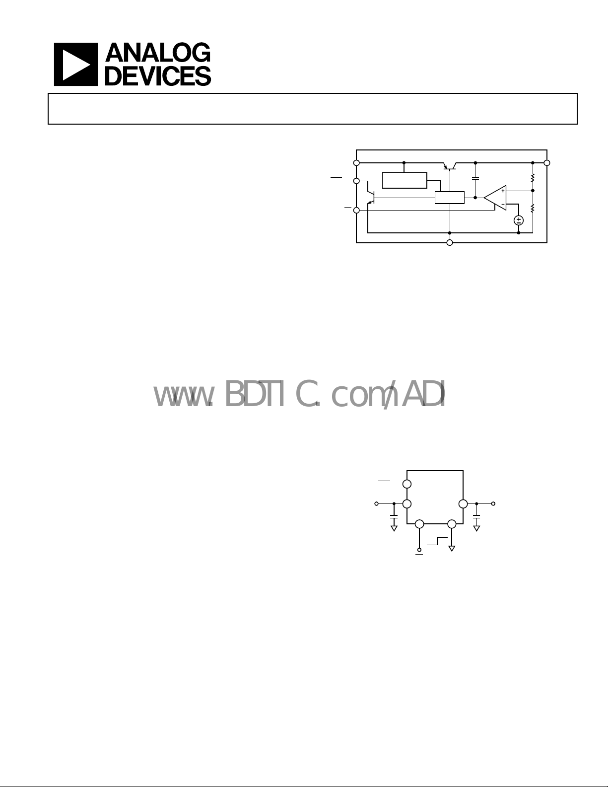
FUNCTIONAL BLOCK DIAGRAM
ADP3309
CC
g
m
BANDGAP
OUTIN
R1
R2
REF
ERR/N
Q1
THERMAL
PROTECTION
Q2
SD
DRIVER
GND
Figure 1.
00141-001
GENERAL DESCRIPTION
The ADP3309 is a member of the ADP330x family of precision
low dropout anyCAP voltage regulators. It is pin-for-pin and
functionally compatible with National’s LP2981, but offers
performance advantages. The ADP3309 stands out from
conventional LDOs with a novel architecture and an enhanced
process. Its patented design requires only a 0.47 μF output
capacitor for stability. This device is stable with any type of
capacitor regardless of its equivalent series resistance (ESR)
value, including ceramic types for space restricted applications.
The ADP3309 achieves ±1.2% accuracy at room temperature
and ±2.2% overall accuracy over temperature, line, and load
regulations. The dropout voltage of the ADP3309 is only
120 mV (typical) at 100 mA. This device also includes a current
limit and a shutdown feature. In shutdown mode, the ground
current is reduced to ~1 μA.
The ADP3309 operates with a wide input voltage range from
2.8 V t
o 12 V and delivers a load current in excess of 100 mA.
The ADP3309 anyCAP LDO offers a wide range of output
voltages.
4
V
IN
0.47µF
ERR/NC
C1
ADP3309-3.3
1
IN
+
–
3
OFF
SD
Figure 2. Typical Application Circuit
ON
OUT
GND
5
+
C2
0.47µF
–
2
V
= 3.3V
OUT
00141-002
Rev. C
Information furnished by Analog Devices is believed to be accurate and reliable. However, no
responsibility is assumed by Anal og Devices for its use, nor for any infringements of patents or ot her
rights of third parties that may result from its use. Specifications subject to change without notice. No
license is granted by implication or otherwise under any patent or patent rights of Analog Devices.
Trademarks and registered trademarks are the property of their respective owners.
One Technology Way, P.O. Box 9106, Norwood, MA 02062-9106, U.S.A.
Tel: 781.329.4700 www.analog.com
Fax: 781.461.3113 ©2006 Analog Devices, Inc. All rights reserved.

ADP3309
www.BDTIC.com/ADI
TABLE OF CONTENTS
Features .............................................................................................. 1
Applications....................................................................................... 1
Functional Block Diagram .............................................................. 1
General Description......................................................................... 1
Revision History ............................................................................... 2
Specifications..................................................................................... 3
Absolute Maximum Ratings............................................................ 4
ESD Caution.................................................................................. 4
Pin Configuration and Function Descriptions............................. 5
Typical Performance Characteristics ............................................. 6
Theory of Operation ........................................................................ 9
Application Information................................................................ 10
REVISION HISTORY
12/06—Rev. B to Rev. C
Change to Table 1 ............................................................................. 3
Updated Outline Dimensions....................................................... 12
Changes to the Ordering Guide.................................................... 12
7/04—Rev. A to Rev. B.
Changes to the Ordering Guide...................................................... 3
Updated Outline Dimensions......................................................... 8
12/00—Rev. 0 to Rev. A
9/98—Revision 0: Initial Version
Capacitor Selection: anyCAP.................................................... 10
Thermal Overload Protection .................................................. 10
Calculating Junction Temperature ........................................... 10
Printed Circuit Board Layout Consideration......................... 10
Shutdown Mode ......................................................................... 10
Error Flag Dropout Detector .................................................... 10
Application Circuits ....................................................................... 11
Crossover Switch ........................................................................ 11
Higher Output Current ............................................................. 11
Constant Dropout Post Regulator............................................ 11
Outline Dimensions ....................................................................... 12
Ordering Guide .......................................................................... 12
Rev. C | Page 2 of 12

ADP3309
www.BDTIC.com/ADI
SPECIFICATIONS
@ TA = −20°C to +85°C, VIN = 7 V, CIN = 0.47 μF, C
options.
Table 1.
Parameter Symbol Conditions Min Typ Max Unit
Output Voltage Accuracy V
I
V
I
Line Regulation
Load Regulation
Ground Current I
I
Ground Current in Dropout I
Dropout Voltage V
I
I
I
Shutdown Threshold V
Off 0.3 V
Shutdown Pin Input Current I
5 < VSD ≤ 12 V @ VIN = 12 V 9 μA
Ground Current in Shutdown Mode IQ VSD = 0 V, VIN = 12 V, TA = 25°C 0.005 1 μA
V
Output Current in Shutdown Mode I
T
Error Pin Output Leakage IEL VEO = 5 V 13 μA
Error Pin Output Low Voltage V
Peak Load Current I
Output Noise @ 5 V Input V
1
Ambient temperature of 85°C corresponds to a junction temperature of 125°C under typical full load test conditions.
= 0.47 μF, unless otherwise noted.1 The following specifications apply to all voltage
OUT
VIN = V
OUT
= 0.1 mA to 100 mA, TA = 25°C
L
= V
IN
= 0.1 mA to 100 mA
L
V
= V
ΔV
OUT
ΔV
IN
ΔV
OUT
ΔI
L
IL = 100 mA 0.8 2.0 mA
GND
VIN = 2.4 V, IL = 0.1 mA 0.9 1.7 mA
GND
V
DROP
On 2.0 V
THSD
0 < VSD ≤ 5 V 1 μA
SDIN
TA = 25°C @ VIN = 12 V 2 μA
OSD
EOL
VIN = V
LDPK
f = 10 Hz to 100 kHz 100 μV rms
NOISE
IN
= 25°C
T
A
I
= 0.1 mA to 100 mA, TA = 25°C 0.06 mV/mA
L
= 0.1 mA 0.19 0.3 mA
L
= 98% of V
OUT
= 100 mA 0.12 0.25 V
L
= 10 mA 0.025 0.07 V
L
= 1 mA 0.004 0.015 V
L
= 0 V, VIN = 12 V, TA = 85°C 0.01 3 μA
SD
= 85°C @ VIN = 12 V 4 μA
A
I
= 400 μA 0.12 0.3 V
SINK
+ 0.3 V to 12 V, −1.2 +1.2 %
OUTNOM
+ 0.3 V to 12 V, −2.2 +2.2 %
OUTNOM
+ 0.3 V to 12 V,
OUTNOM
OUTNOM
+ 1 V, TA = 25°C 150 mA
OUTNOM
0.02 mV/V
Rev. C | Page 3 of 12

ADP3309
www.BDTIC.com/ADI
ABSOLUTE MAXIMUM RATINGS
Table 2.
Parameter Rating
Input Supply Voltage −0.3 V to +16 V
Shutdown Input Voltage −0.3 V to +16 V
Power Dissipation Internally Limited
Operating Ambient Temperature Range −55°C to +125°C
Operating Junction Temperature Range −55°C to +125°C
θ
JA
θ
JC
Storage Temperature Range −65°C to +150°C
Lead Temperature (Soldering 10 sec) 300°C
Vapor Phase (60 sec) 215°C
Infrared (15 sec) 220°C
190°C/W
92°C/W
Stresses above those listed under Absolute Maximum Ratings
may cause permanent damage to the device. This is a stress
rating only; functional operation of the device at these or any
other conditions above those indicated in the operational
section of this specification is not implied. Exposure to absolute
maximum rating conditions for extended periods may affect
device reliability.
ESD CAUTION
Rev. C | Page 4 of 12
 Loading...