Analog Devices ADP3303A Datasheet

High Accuracy anyCAP™ Adjustable
ADP3303A
ERR
OUT
IN
FB
R1
C2
1mF
V
OUT
= +5V
ON
OFF
SD
GND
C1
0.47mF
V
IN
R2
R3
330kV
E
OUT
SD
a
FEATURES
High Accuracy Over Line and Load:
ⴞ0.8% @ +25ⴗC, ⴞ1.4% Over Temperature
Ultralow Dropout Voltage: 150 mV Typical @ 200 mA
Requires Only C
anyCAP = Stable with All Types of Capacitors
(Including MLCC)
Current and Thermal Limiting
Low Noise
Dropout Detector
Low Shutdown Current: 1 A
3.2 V to 12 V Supply Range
Adjustable 2.2 V to 10 V Output Range
–20ⴗC to +85ⴗC Ambient Temperature Range
Thermally Enhanced TSSOP-14 Package
APPLICATIONS
Cellular Telephones
Notebook, Palmtop Computers
Battery Powered Systems
Portable Instruments
Post Regulator for Switching Supplies
Bar Code Scanners
= 1 F for Stability
O
200 mA Low Dropout Linear Regulator
ADP3303A
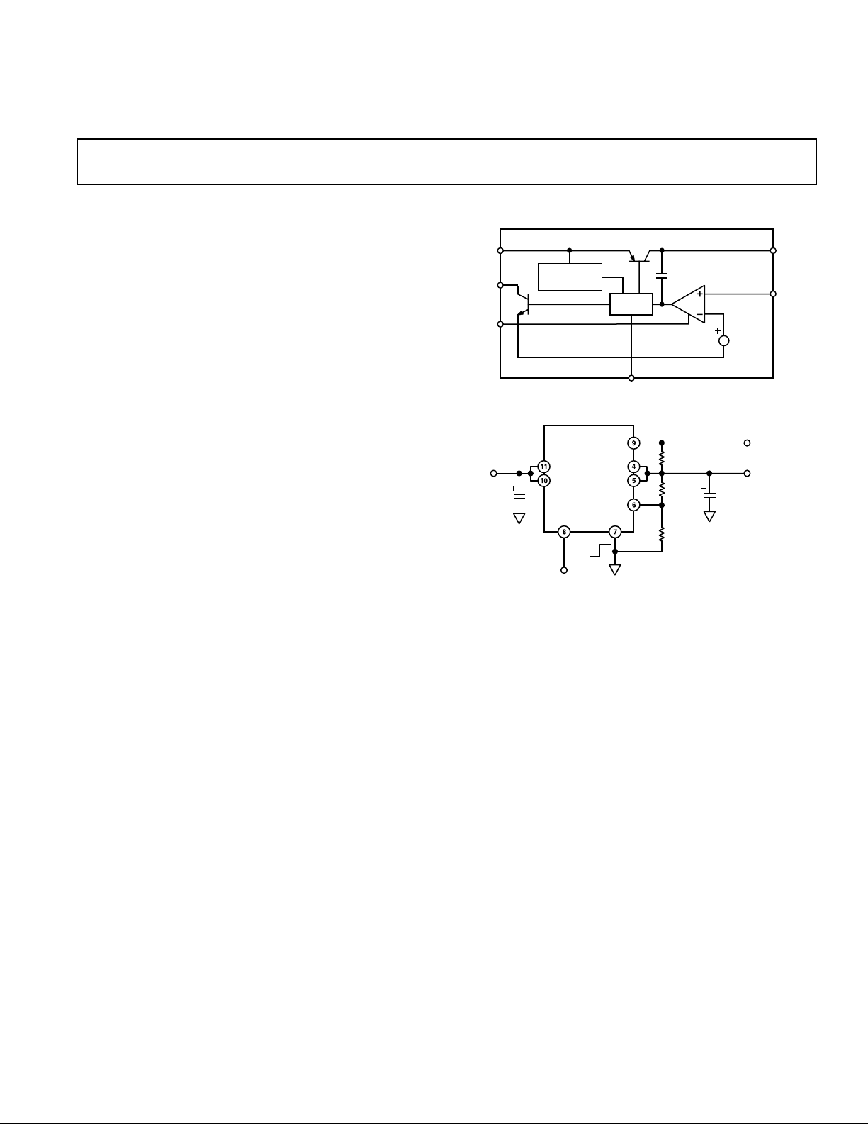
FUNCTIONAL BLOCK DIAGRAM
ADP3303A
CC
g
m
BANDGAP
REF
OUT
FB
ERR
SD
IN
THERMAL
PROTECTION
Q2
Q1
DRIVER
GND
Figure 1. Typical Application Circuit
GENERAL DESCRIPTION
The ADP3303A is a member of the ADP330x family of precision low dropout anyCAP voltage regulators. The ADP3303A
stands out from conventional LDOs with a novel architecture,
an enhanced process and a new package. Its patented design
requires only a 1 µF output capacitor for stability. This device is
insensitive to output capacitor ESR (Equivalent Series Resistance), and is stable with any good quality capacitor, including
ceramic types (MLCC) for space restricted applications. The
ADP3303A achieves exceptional accuracy of ±0.8% at room
temperature and ±1.4% overall accuracy over temperature, line
and load variations. The dropout voltage of the ADP3303A is
only 150 mV (typical) at 200 mA.
anyCAP is a trademark of Analog Devices Inc.
REV. A
Information furnished by Analog Devices is believed to be accurate and
reliable. However, no responsibility is assumed by Analog Devices for its
use, nor for any infringements of patents or other rights of third parties
which may result from its use. No license is granted by implication or
otherwise under any patent or patent rights of Analog Devices.
In addition to the new architecture and process, ADI’s new
proprietary thermally enhanced package (Thermal Coastline)
can handle 1 W of power dissipation without an external heat
sink or large copper surface on the PC board. This keeps PC
board real estate to a minimum and makes the ADP3303A very
attractive for use in portable equipment.
The ADP3303A operates over an input voltage range of 3.2 V
to 12 V and delivers a load current in excess of 200 mA. The
output voltage can be adjusted from 2.2 V to 10 V using an
external resistor divider. It also features an error flag that signals
when the device is about to lose regulation or when the short
circuit or thermal overload protection is activated. Other features include shutdown and optional noise reduction capabilities.
One Technology Way, P.O. Box 9106, Norwood, MA 02062-9106, U.S.A.
Tel: 781/329-4700 World Wide Web Site: http://www.analog.com
Fax: 781/326-8703 © Analog Devices, Inc., 1999

ADP3303A–SPECIFICATIONS
(@ TA = –20ⴗC to +85ⴗC, VIN = 7 V, CIN = 0.47 F, C
1
noted)
= 1 F, unless otherwise
OUT
Parameter Symbol Conditions Min Typ Max Units
OUTPUT VOLTAGE
ACCURACY I
2, 3, 4
V
OUT
VIN = Nom V
= 1.0 mA to 200 mA
L
T
= +25°C –0.8 +0.8 %
A
V
= Nom V
IN
+0.5 V to +12 V
OUT
+0.5 V to +12 V
OUT
IL = 1.0 mA to 200 mA –1.4 +1.4 %
LINE REGULATION ∆V
∆V
LOAD REGULATION ∆V
∆I
GROUND CURRENT
5
I
GND
O
IN
O
L
VIN = Nom V
T
= +25°C 0.01 mV/V
A
+0.5 V to +12 V
OUT
IL = 1.0 mA to 200 mA
T
= +25°C 0.005 mV/mA
A
IL = 200 mA 2.0 4 mA
IL = 1.0 mA 0.35 0.6 mA
GROUND CURRENT
5
I
GND
VIN = 2.5 V, V
OUT
= 5.0 V
IN DROPOUT IL = 1.0 mA 1.9 3.0 mA
V
DROPOUT VOLTAGE V
DROP
≤ 98% of VO Nominal
OUT
I
= 200 mA 0.15 0.4 V
L
I
= 10 mA 0.02 0.07 V
L
IL = 1 mA 0.003 0.03 V
SHUTDOWN THRESHOLD V
THSD
ON 2.0 0.9 V
OFF 0.9 0.3 V
SHUTDOWN PIN I
SDIN
0 V < VSD
≤
5 V 1 µA
INPUT CURRENT 5 V ≤ VSD ≤ 12 V @ VIN = 12 V 22 µA
GROUND CURRENT IN
5
SHUTDOWN MODE T
OUTPUT CURRENT IN I
SHUTDOWN MODE T
I
Q
OSD
VSD = 0, VIN = 12 V
= +25°C1µA
A
V
= 0 V, VIN = 12 V
SD
T
= +85°C5µA
A
T
= +25°C @ VIN = 12 V 2.5 µA
A
= +85°C @ VIN = 12 V 4 µA
A
ERROR PIN OUTPUT
LEAKAGE I
EL
V
= 5 V 13 µA
EO
ERROR PIN OUTPUT
“LOW” VOLTAGE V
PEAK LOAD CURRENT I
OUTPUT NOISE V
EOL
LDPK
NOISE
@ 5 V OUTPUT C
NOTES
1
Ambient temperature of +85°C corresponds to a typical junction temperature of +125°C under typical full load test conditions. The formula for Nom V
in the Output Voltage Selection section.
2
Accuracy guaranteed using external trim pots.
3
For 2.7 V output, the minimum VIN is 3.2 V.
4
Guaranteed by design and characterization.
5
Ground currents include the current through R1, R2.
Specifications subject to change without notice.
I
= 400 µA 0.15 0.3 V
SINK
VIN = Nom V
+ 1 V 300 mA
OUT
f = 10 Hz–100 kHz
= 0 100 µV
NR
CNR = 10 nF, C
= 10 µF30µV
L
OUT
rms
rms
is found
–2–
REV. A

ADP3303A
WARNING!
ESD SENSITIVE DEVICE
ABSOLUTE MAXIMUM RATINGS*
Input Supply Voltage . . . . . . . . . . . . . . . . . . . –0.3 V to +16 V
Shutdown Input Voltage . . . . . . . . . . . . . . . . –0.3 V to +16 V
Error Flag Output Voltage . . . . . . . . . . . . . . . –0.3 V to +16 V
Noise Bypass Pin Voltage . . . . . . . . . . . . . . . . –0.3 V to +5 V
Power Dissipation . . . . . . . . . . . . . . . . . . . Internally Limited
Operating Ambient Temperature Range . . . –55°C to +125°C
Operation Junction Temperature Range . . . –55°C to +125°C
. . . . . . . . . . . . . . . . . . . . . . . . . . . . . . . . . . . . . 96°C/W
θ
JA
Storage Temperature Range . . . . . . . . . . . . –65°C to +150°C
Lead Temperature Range (Soldering 10 sec) . . . . . . . +300°C
Vapor Phase (60 sec) . . . . . . . . . . . . . . . . . . . . . . . +215°C
Infrared (15 sec) . . . . . . . . . . . . . . . . . . . . . . . . . . +220°C
*This is a stress rating only; operation beyond these limits can cause the device to
be permanently damaged.
Other Members of anyCAP Family
Output Package
Model Current Options
2
1
Comments
ADP3300 50 mA SOT-23-6 High Accuracy
ADP3301 100 mA SO-8 High Accuracy
ADP3302 100 mA SO-8 Dual Output
ADP3307 100 mA SOT-23-6 High Accuracy
ADP3308 50 mA SOT-23-5 High Accuracy
ADP3309 100 mA SOT-23-5 High Accuracy
NOTES
1
See individual data sheets for detailed ordering information.
2
SO = Small Outline, SOT = Surface Mount Outline.
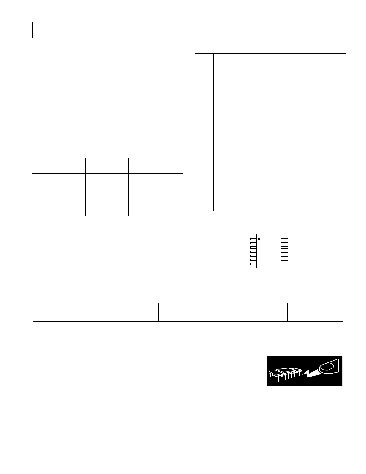
PIN FUNCTION DESCRIPTIONS
Pin Mnemonic Function
1–3 NC No Connect.
4 & 5 OUT Output of the Regulator. Bypass to
ground with a 1 µF or larger capacitor.
Pins 4 and 5 must be connected
together for proper operation.
6 FB Feedback. Connect to an external
resistor divider that sets the output
voltage.
7 GND Ground.
8 SD Active Low Shutdown Pin. Connect to
ground to disable the regulator output.
When shutdown is not used, this pin
should be connected to the input pin.
9 ERR Open Collector Output that goes low to
indicate that the output is about to go
out of regulation.
10 & 11 IN Regulator Input. Pins 10 and 11 must
be connected together for proper
operation.
12–14 NC No Connect.
PIN CONFIGURATION
NC
NC
NC
OUT
OUT
FB
GND
NC = NO CONNECT
ADP3303A
TOP VIEW
(Not to Scale)
NC
NC
NC
IN
IN
ERR
SD
ORDERING GUIDE
Model Voltage Output Package Description Package Option
ADP3303AARU-Reel ADJ Thin Shrink Small Outline Package (TSSOP) TSSOP-14
NOTES
All devices operate over the ambient temperature range of –20°C to +85°C.
Contact the factory for the availability of other output voltage options.
CAUTION
ESD (electrostatic discharge) sensitive device. Electrostatic charges as high as 4000 V readily
accumulate on the human body and test equipment and can discharge without detection.
Although the ADP3303A features proprietary ESD protection circuitry, permanent damage may
occur on devices subjected to high energy electrostatic discharges. Therefore, proper ESD
precautions are recommended to avoid performance degradation or loss of functionality.
REV. A
–3–
 Loading...