High Precision anyCAP™
ADP3302
7
6
2
OUT1
IN
1
5
ERR
330kΩ
E
OUT
0.47µF
V
OUT1
ON
OFF
0.47µF
8
V
IN
GND
SD1
3
IN
4
OUT2
0.47µF
V
OUT2
SD2
a
Dual Low Dropout Linear Regulator
FEATURES
High Accuracy: 60.8%
Ultralow Dropout Voltage: 120 mV @ 100 mA Typical
Requires only C
= 0.47 mF for Stability
O
anyCAP™ = Stable with All Types of Capacitors
Current and Thermal Limiting
Low Noise
Dropout Detector
Multiple Voltage Options
Thermally Enhanced SO-8 Package
APPLICATIONS
Cellular Telephones
Notebook and Palmtop Computers
Battery Powered Systems
Portable Instruments
High Efficiency Linear Regulators
GENERAL DESCRIPTION
The ADP3302 is a member of the ADP330X family of precision
micropower low dropout anyCAP™ regulators. The ADP3302
contains two fully independent 100 mA regulators with separate
shutdown and merged error outputs. It features 1.4% overall
output accuracy and very low, 120 mV typical, dropout voltage.
The ADP3302 has a wide input voltage range from 13 V to
112 V. It features an error flag that signals when either of the
two regulators is about to lose regulation. It has short circuit
current protection as well as thermal shutdown.
The ADP3302’s enhanced lead frame design allows for a maximum power dissipation of 630 mW @ +70°C ambient temperature
and 1.0 W at room temperature without any external heat sink.
ERR
SD
ADP3302
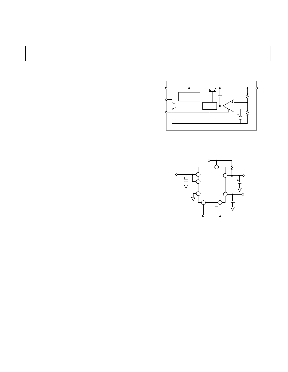
FUNCTIONAL BLOCK DIAGRAM
(1/2 IS SHOWN)
IN
THERMAL
PROTECTION
Q2
Q1
DRIVER
GND
Figure 1. Application Circuit
ADP3302
CC
GM
BANDGAP
REF
OUT
R1
R2
anyCAP™ is a trademark of Analog Devices, Inc.
REV. 0
Information furnished by Analog Devices is believed to be accurate and
reliable. However, no responsibility is assumed by Analog Devices for its
use, nor for any infringements of patents or other rights of third parties
which may result from its use. No license is granted by implication or
otherwise under any patent or patent rights of Analog Devices.
One Technology Way, P.O. Box 9106, Norwood, MA 02062-9106, U.S.A.
Tel: 617/329-4700 World Wide Web Site: http://www.analog.com
Fax: 617/326-8703 © Analog Devices, Inc., 1997

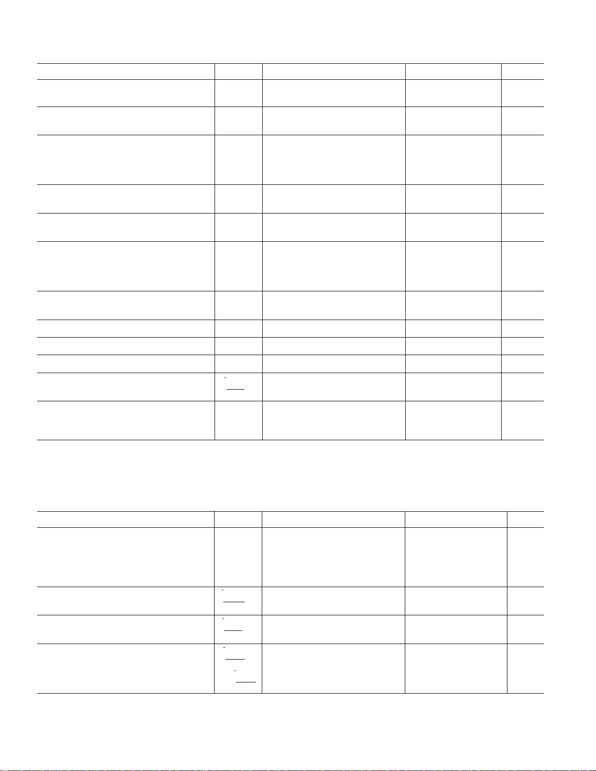
ADP3302–SPECIFICATIONS
(@ TA = –208C to +858C, VIN = 7 V, CIN = 0.47 mF, C
1
noted)
= 0.47 mF, unless otherwise
OUT
Parameter Symbol Conditions Min Typ Max Units
GROUND CURRENT I
GND
IL1 = IL2 = 100 mA 2 4 mA
IL1 = IL2 = 0.1 mA 0.4 0.8 mA
GROUND CURRENT IN DROPOUT I
GND
VIN = 2.5 V 1.0 2 mA
IL1 = IL2 = 0.1 mA
DROPOUT VOLTAGE V
DROP
V
OUT
I
= 100 mA 0.12 0.2 V
L
I
= 10 mA 0.05 0.1 V
L
IL = 1 mA 0.02 0.05 V
SHUTDOWN THRESHOLD V
THSD
ON 2.0 0.9 V
OFF 0.9 0.3 V
SHUTDOWN PIN INPUT CURRENT I
SDIN
0 < V
5 ≤ V
GROUND CURRENT IN SHUTDOWN I
Q
V
SDI
MODE @ V
V
SDI
@ V
OUTPUT CURRENT IN SHUTDOWN I
OSD
MODE T
ERROR PIN OUTPUT LEAKAGE I
ERROR PIN OUTPUT “LOW” VOLTAGE V
PEAK LOAD CURRENT I
THERMAL REGULATION V
OUTPUT NOISE V
NOTES
1
Ambient temperature of 185°C corresponds to a typical junction temperature of
Specifications subject to change without notice.
EL
EOL
LDPK
∆V
V
NOISE
O
O
T
= +85°C, @ VIN = 12 V 12 µA
A
= +25°C, @ VIN = 12 V 2 µA
A
V
= 5 V 13 µA
EO
I
SINK
VIN = Nominal V
= 12 V, IL = 100 mA 0.05 %/W
IN
T = 10 ms
f = 10 Hz–100 kHz, @ T
V
OUT
V
OUT
≤ 98% of V
< 5 V 0 1 µA
SD
≤ 12 V, @ VIN = 12 V 22 µA
SD
= V
SD2
=12 V 0 1 µA
IN
= V
SD2
=12 V 5 µA
IN
= 0, T
= 0, T
, Nominal
O
= +25°C,
A
= +85°C,
A
= 400 µA 0.15 0.3 V
+1 V 200 mA
OUT
= +25°C
A
= 3.3 V 75 µV rms
= 5 V 110 µV rms
+125°C.
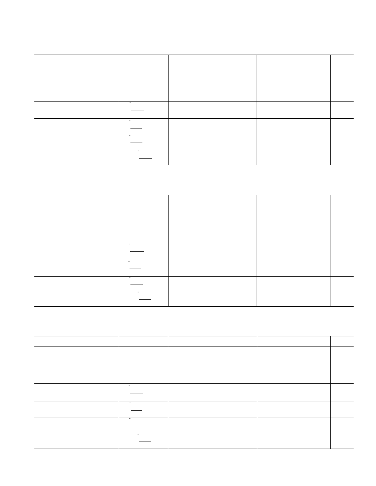
ADP3302-3.0–SPECIFICATIONS
(@ TA = –208C to +858C, VIN = 3.3 V, CIN = 0.47 mF, C
otherwise noted)
= 0.47 mF, unless
OUT
Parameter Symbol Conditions Min Typ Max Units
OUTPUT VOLTAGE V
or VIN = 3.3 V to 12 V 2.976 3 3.024 V
OUT1
V
OUT2
IL = 0.1 mA to 100 mA
T
= +25°C
A
V
= 3.3 V to 12 V 2.958 3 3.042 V
IN
IL = 0.1 mA to 100 mA
∆V
or
∆V
∆V
∆I
∆V
∆I
IN
O
L
L2
∆V
O
01
∆I
= 3.3 V to 12 V 0.024 mV/V
IN
T
= +25°C, I
A
T
= +25°C
A
= 0.1 mA to 100 mA 1 µV/mA
L
T
= +25°C
A
02
L1
–2–
= 0.1 mA
L
REV. 0
LINE REGULATION V
LOAD REGULATION IL = 0.1 mA to 100 mA 0.030 mV/mA
CROSS REGULATION I
Specifications subject to change without notice.

ADP3302
(@ TA = –208C to +858C, VIN = 3.5 V, CIN = 0.47 mF, C
ADP3302-3.2–SPECIFICATIONS
otherwise noted)
Parameter Symbol Conditions Min Typ Max Units
= 0.47 mF, unless
OUT
OUTPUT VOLTAGE V
or VIN = 3.5 V to 12 V 3.174 3.2 3.226 V
OUT1
V
OUT2
IL = 0.1 mA to 100 mA
T
= +25°C
A
V
= 3.5 V to 12 V 3.155 3.2 3.245 V
IN
IL = 0.1 mA to 100 mA
∆V
∆V
∆V
∆I
or
∆V
∆I
L2
O
L
01
O
IN
∆V
∆I
02
L1
LINE REGULATION V
LOAD REGULATION I
CROSS REGULATION I
Specifications subject to change without notice.
ADP3302-3.3–SPECIFICATIONS
= 3.5 V to 12 V 0.026 mV/V
IN
T
= +25°C, I
A
= 0.1 mA to 100 mA 0.032 mV/mA
L
T
= +25°C
A
= 0.1 mA to 100 mA 1 µV/mA
L
T
= +25°C
A
(@ TA = –208C to +858C, VIN = 3.6 V, CIN = 0.47 mF, C
= 0.1 mA
L
= 0.47 mF, unless
OUT
otherwise noted)
Parameter Symbol Conditions Min Typ Max Units
OUTPUT VOLTAGE V
or VIN = 3.6 V to 12 V 3.273 3.3 3.327 V
OUT1
V
OUT2
IL = 0.1 mA to 100 mA
T
= +25°C
A
V
= 3.6 V to 12 V 3.253 3.3 3.347 V
IN
IL = 0.1 mA to 100 mA
∆V
∆V
∆V
or
∆V
∆I
∆I
O
L
L2
O
IN
01
∆V
∆I
= 3.6 V to 12 V 0.026 mV/V
IN
T
= +25°C, I
A
= 0.1 mA to 100 mA 0.033 mV/mA
L
T
= +25°C
A
= 0.1 mA to 100 mA 1 µV/mA
L
T
= +25°C
A
02
L1
(@ TA = –208C to +858C, VIN = 5.3 V, CIN = 0.47 mF, C
= 0.1 mA
L
= 0.47 mF, unless
OUT
otherwise noted)
LINE REGULATION V
LOAD REGULATION I
CROSS REGULATION I
Specifications subject to change without notice.
ADP3302-5.0–SPECIFICATIONS
Parameter Symbol Conditions Min Typ Max Units
OUTPUT VOLTAGE V
or VIN = 5.3 V to 12 V 4.960 5.0 5.040 V
OUT1
V
OUT2
IL = 0.1 mA to 100 mA
T
= +25°C
A
V
= 5.3 V to 12 V 4.930 5.0 5.070 V
IN
IL = 0.1 mA to 100 mA
∆V
∆V
∆V
∆I
∆V
∆I
or
IN
L
L2
O
O
01
∆V
∆I
= 5.3 V to 12 V 0.04 mV/V
IN
T
= +25°C, I
A
= 0.1 mA to 100 mA 0.05 mV/mA
L
T
= +25°C
A
= 0.1 mA to 100 mA 1 µV/mA
L
T
= +25°C
A
02
L1
= 0.1 mA
L
–3–
LINE REGULATION V
LOAD REGULATION I
CROSS REGULATION I
Specifications subject to change without notice.
REV. 0
 Loading...