

3-Phase IMVP-II and IMVP-III
a
FEATURES
Pin Selectable 1-, 2-, or 3-Phase Operation
Static and Dynamic Current Sharing Characteristics
Backward Compatible to IMVP-II
Superior Load Transient Response with ADOPT
Analog Devices’ Optimal Positioning Technology
Noise-Blanking for Speed and Stability
Synchronous Rectifier Control Extends Battery Life
Smooth Output Transition During VID Code Change
Cycle-by-Cycle Current Limiting
Hiccup or Latched Overload Protection
Transient-Glitch-Free Power Good
Soft Start Eliminates Power-On In-Rush Current Surge
Two-Level Overvoltage and Reverse Voltage
Protection
APPLICATIONS
IMVP-II and IMVP-III Core DC-to-DC Converters
Fixed Voltage Mobile CPU Core DC-to-DC Converters
Notebook/Laptop Power Supplies
Programmable Output Power Supplies
®
Core Controller for Mobile CPUs
*
OUT3
OUT2
OUT1
CS3
CS2
CS1
CS+
CS–
RAMP
REG
DACOUT
DACRAMP
HYSSET
DSHIFT
BSHIFT
DPRSHIFT
VID4
VID3
VID2
VID1
VID0
ADP3204
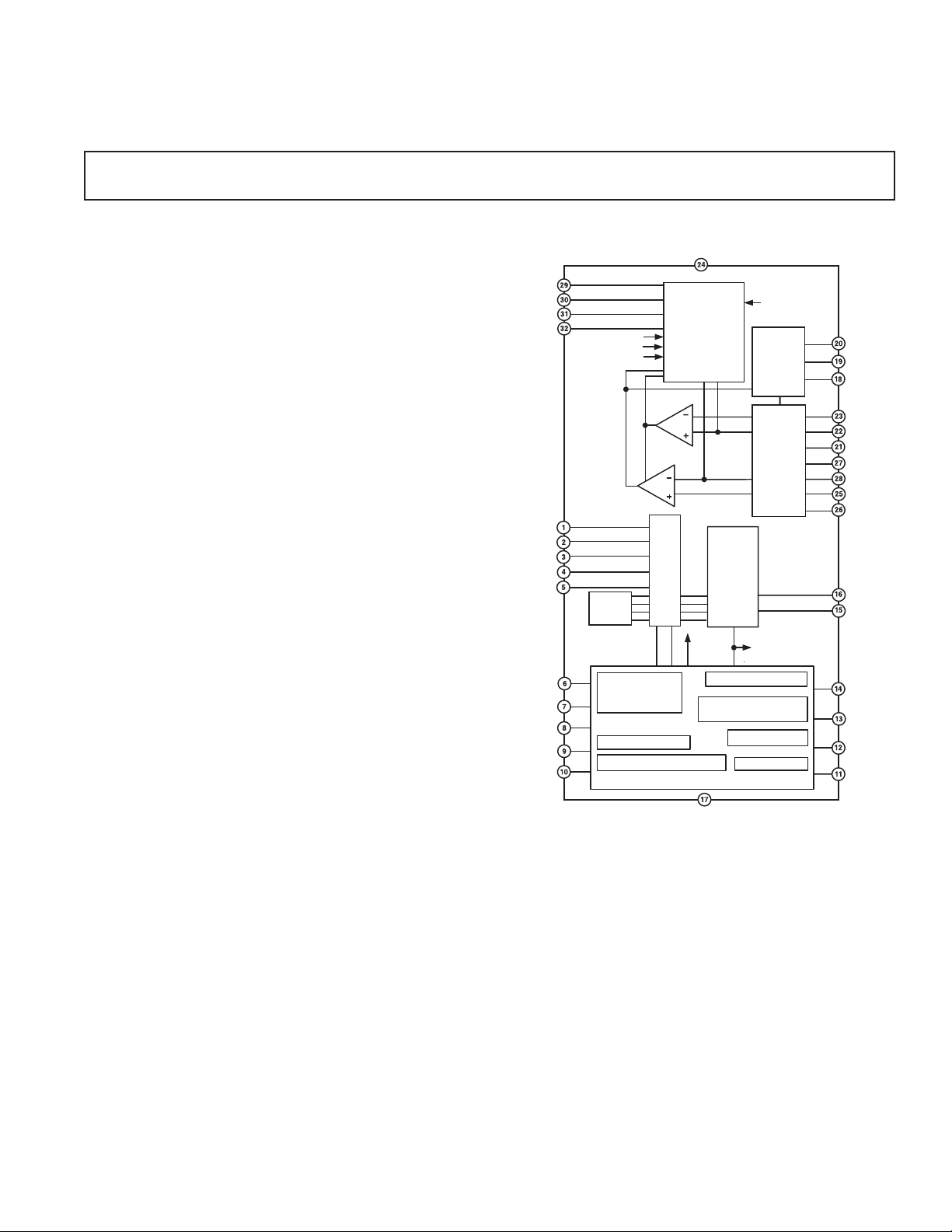
FUNCTIONAL BLOCK DIAGRAM
VCC
ADP3204
DAC
AND
FIXED
REF
VR
PHASE
SPLITTER
CURRENT
SENSE
MUX
DPSLP
DPRSLP
DPRSLP
VID
GEN
BOM
EN
CORE
VID
MUX
AND
REG
HYSTERESIS
SETTING
AND
SHIFT-MUX
CLIM
5-BIT VID
GENERAL DESCRIPTION
The ADP3204 is a 1-, 2-, or 3-phase hysteretic peak current
dc-to-dc buck converter controller dedicated to power a mobile
processor’s core. The optimized low voltage design is powered
from the 3.3 V system supply. The nominal output voltage is
set by a 5-bit VID code. To accommodate the transition time
required by the newest processors, the ADP3204 features
high speed operation to allow a minimized inductor size that
results in the fastest change of current to the output. To
further allow for the minimum number of output capacitors
to be used, the ADP3204 features active voltage positioning
with ADOPT
optimal compensation to ensure a superior
load transient response. The output signals interface with a
maximum of three ADP3415 MOSFET drivers that are
optimized for high speed and high efficiency for driving both the
top and bottom MOSFETs of the buck converter. The
ADP3204 is capable of controlling the synchronous rectifiers to
extend battery lifetime in light load conditions.
ADOPT is a trademark of Analog Devices, Inc.
*Protected by U.S.Patent No. 5,969,657; other patents pending.
REV. 0
Information furnished by Analog Devices is believed to be accurate and
reliable. However, no responsibility is assumed by Analog Devices for its
use, nor for any infringements of patents or other rights of third parties that
may result from its use. No license is granted by implication or otherwise
under any patent or patent rights of Analog Devices.
DPSLP
DPRSLP
BOM
BOM
DPSLP
DPRSLP
PWRGD
SD
One Technology Way, P.O. Box 9106, Norwood, MA 02062-9106, U.S.A.
Tel: 781/329-4700 www.analog.com
Fax: 781/326-8703 © Analog Devices, Inc., 2002
VID TRANSIENT
DETECTOR AND
SHIFT SELECTOR
PWRGD BLANKER
ENABLE UVLO-MAIN BIAS
PM MODULE
GND
VR
COREGD MONITOR
SS-HICCUP TIMER
AND OCP
SR CONTROL
OVP AND RVP
COREFB
SS
DRVLSD
CLAMP

ADP3204–SPECIFICATIONS
100 k, C
OUT1
= C
OUT2
= C
=10 pF, CSS = 0.047 F, R
OUT3
PWRGD
(0°C ⱕ TA ⱕ 100°C, High (H) = VCC, Low (L) = 0 V, VCC = 3.3 V, SD = H, V
V
DAC (VDACOUT
= 680 to 1.2 V, R
), V
REG
= V
= V
CS–
CLAMP
= 1.25 V, C
VID
= 5.1 k to VCC, HYSSET, BSHIFT, DSHIFT, and
DACRAMP
= 100 pF, R
OUT1
= R
OUT2
COREFB
= R
OUT3
=
=
1
DPRSHIFT are open, BOM = H, DPSLP = H, DPRLP = L, unless otherwise noted.) Current sunk by a pin has a positive sign, sourced by a pin has a
negative sign. Negative sign is disregarded for min and max values.
Parameter Symbol Conditions Min Typ Max Unit
SUPPLY-UVLO-SHUTDOWN
Normal Supply Current I
UVLO Supply Current I
Shutdown Supply Current I
CC
CCUVLO
CCSD
SD = L, 3.0 V ≤ VCC ≤ 3.6 V 70 A
711 mA
425 A
UVLO Threshold SD = H
VCC ramping up, VSS = 0 V 2.95 V
VCC ramping down, 2.60 V
V
floating
SS
55 mV
UVLO Hysteresis V
V
CCH
V
CCL
CCHYS
Shutdown Threshold
(CMOS Input) V
SDTH
VCC/2 V
POWER GOOD
Core Feedback Threshold Voltage V
Power Good Output Voltage V
(Open-Drain Output) V
Masking Time
2
COREFBH
PWRGD
t
PWRGDMSK
3
0.9 V < V
V
V
V
V
V
ramping up 1.12 V
COREFB
ramping down 1.10 V
COREFB
ramping up 0.88 V
COREFB
ramping down 0.86 V
COREFB
= V
COREFB
= 0.8 V
COREFB
< 1.675 V
DAC
DACOUT
DACOUT
1.14 V
1.12 V
0.90 V
0.88 V
V
CC
DAC
DAC
DAC
DAC
0.95 V
DAC
DAC
DAC
DAC
CC
0 0.8 V
100 s
V
V
V
V
V
SOFT START/HICCUP TIMER
Charge/Discharge Current I
Soft Start Enable/Hiccup V
SS
SSEN
Termination Threshold V
Soft Start Termination/Hiccup V
SSTERM
VSS = 0 V –55 A
V
= 0.5 V 1.2 A
SS
V
= 1.25 V,
REG
= V
RAMP
V
ramping down 200 300 mV
SS
V
= V
RAMP
COREFB
COREFB
= 1.27 V
= 1.27 V
Enable Threshold VSS ramping up 1.70 2.00 2.25 V
VID DAC
VID Input Threshold V
VID0..4
VCC/2 V
(CMOS Inputs)
VID Input Current I
VID0..4
VID0 to VID4 = L 85 A
(Internal Active Pull-Up)
Output Voltage V
Accuracy ⌬V
Settling Time t
DACRAMP Inner Resistance
5
DACS
R
DAC
DAC/VDAC
4
DACRAMP
See VID Code, Table 1 0.600 1.750 V
1.750 V ≥ V
0.825 V ≥ V
C
DACRAMP
C
DACRAMP
≥ 0.850 V –1.0 +1.0 %
DAC
≥ 0.600 V –8.5 +8.5 mV
DAC
= 100 pF 3.5 s
= 1 nF 25 s
10 k⍀
REV. 0–2–

ADP3204
Parameter Symbol Conditions Min Typ Max Unit
CORE COMPARATOR
Input Offset Voltage (Ramp-Reg) V
Input Bias Current I
Output Voltage V
(OUT1, OUT2, and OUT3) V
Propagation Delay Time t
Rise and Fall Time t
(OUT1, OUT2, and OUT3) t
Noise Blanking Time t
COREOS
, I
REG
RAMP
OUT_H
OUT_L
RMPOUT_PD
7
OUT_R
7
OUT_F
BLNK
CURRENT LIMIT COMPARATOR
Input Offset Voltage V
Input Bias Current I
Propagation Delay Time t
CLIMOS
, I
CS+
CLPD
6
CS–
CURRENT SENSE
MULTIPLEXER
Trans-Resistance R
R
R
, MUX switch is ON 150 ⍀
CS1–CS+
, MUX switch is OFF 50 M⍀
CS2–CS+
CS3–CS+
Common-Mode Voltage Range V
HYSTERESIS SETTING
Hysteresis Current I
–I
Hysteresis Reference Voltage V
,V
RAMP_H
CS+_H
HYSSET
CURRENT LIMIT SETTING
Hysteresis Current I
CS–
V
= 1.25 V ± 1.5 mV
REG
V
REG
= V
= 1.25 V ±1 A
RAMP
VCC = 3.0 V 2.5 3.0 V
VCC = 3.6 V 0 0.4 V
6
TA = 25°C35ns
T
= Full Range 45 ns
A
7ns
7ns
OUT L-H Transition 70 ns
OUT H-L Transition 130 ns
VCS– = 1.25 V ± 1mV
V
= 1.25 V –3 A
CS+
TA = 25° C55ns
TA = Full Range 65 ns
= V
= V
CS2
= 1.25 V
= 1.23 V
= 10 A–8–10 –12 A
= 100 A –85 –100 –115 A
= 1.27 V
= 10 A81012 A
= 100 A85100 115 A
= 1.23 V
= V
= V
CS–
= 1.23 V
= 10 A –27 –31.5 –36 A
= 100 A –270 –301.5 –333 A
= 1.27 V
= 10 A –18 –21.5 –25 A
= 100 A –180 –201.5 –223 A
= 1.23 V, BOM = L
V
V
V
V
V
V
V
CS1
REG
RAMP
I
HYSSET
I
HYSSET
RAMP
I
HYSSET
I
HYSSET
RAMP
REG
CS+
I
HYSSET
I
HYSSET
CS+
I
HYSSET
I
HYSSET
CS+
CS3
COREFB
= 1.25 V
02V
V
DAC
V
REV. 0
–3–

ADP3204
Parameter Symbol Conditions Min Typ Max Unit
SHIFT SETTING
Battery-Shift Current I
Battery-Shift Reference Voltage V
RAMPB
BSHIFT
, I
CS+BVVID
= 1.25 V –92.5 –100 –107.5 mA
= –100 µA, BOM = L
I
BSHIFT
DPSLP = H
V
DAC
V
Deep Sleep-Shift Current I
RAMPD
, I
CS+DVVID
= 1.25 V –92.5 –100 –107.5 mA
I
= –100 µA, BOM = H
DSHIFT
DPSLP = L
Deep Sleep-Shift Reference V
DSHIFT
V
DAC
V
Voltage
Deeper Sleep-Shift Current I
REGDPR
I
COREFBDPR
8
I
DPRSHIFT
V
I
DPRSHIFT
= –100 µA, DPRSLP = H –90 –100 –110 µA
= 1.25 V, 110 130 150 µA
VID
= –100 µA,
DPRSLP = H
Deeper Sleep-Shift Reference V
DPRSHIFT
V
DAC
V
Voltage
SHIFT CONTROL INPUTS
BOM Threshold V
BOM
VCC/2 V
(CMOS Input)
DPSLP Threshold V
(CMOS Input)
DPRSLP Mode Threshold
8
DSLP
V
DPRSLP
VCC/2 V
VCC/2 V
(CMOS Input)
LOW SIDE DRIVE CONTROL
Output Voltage (CMOS Output) V
Output Current I
DRVLSD
DRVLSD
DPRSLP = H 0 0.4 V
DPRSLP = L 0.7 V
DPRSLP = H, V
DPRSLP = L, V
= 1.5 V +0.4 mA
DRVLSD
= 1.5 V –0.4 mA
DRVLSD
CC
V
CC
V
OVER/REVERSE VOLTAGE
PROTECTION CORE FEEDBACK
Overvoltage Threshold V
Reverse-Voltage Threshold V
Output Current I
COREFB, OVP
COREFB, RVP
CLAMP
(Open-Drain Output) V
NOTES
1
All limits at temperature extremes are guaranteed via correlation using standard Statistical Quality Control (SQC) methods.
2
Two test conditions: 1) PWRGD is OK but forced to fail by applying an out-of-the-Core Good-window voltage (V
COREFB pin right after the moment that BOM or DPRSLP is asserted/de-asserted. PWRGD should not fail immediately only with the specified blanking delay
time. 2) PWRGD is forced to fail (V
that BOM or DPRSLP is asserted/de-asserted. PWRGD should not go high immediately only with the specified blanking delay time.
3
Guaranteed by design
4
Measured from 50% of VID code transition amplitude to the point where V
5
Measured between DACRAMP and DACOUT pins.
6
40 mVpp amplitude impulse with 20 mV overdrive. Measured from the input threshold intercept point to 50% of the output voltage swing.
7
Measured between the 30% and 70% points of the output voltage swing.
8
DPRSLP circuit meets the minimum 30 ns DPRSLPVR signal assertion requirement; guaranteed by design.
9
COREFB pin has a resistor divider to GND whose resistance is 41.3 k⍀ (typ), guaranteed by design.
COREFB, BAD
= 1.0 V at V
9
V
COREFB
9
V
COREFB
V
= 1.25 V setting) but gets into the Core Good-window (V
VID
= 2.2 V, V
COREFB
= V
COREFB
settles within ± 1% of its steady state value.
DACOUT
DAC
, V
= 1.5 V 10 µA
CLAMP
= 1.5 V 2 6 mA
CLAMP
COREFB, BAD
= 1.0 V at V
COREFB, GOOD
2.0 V
–0.3 V
= 1.25 V setting) to the
VID
= 1.25 V) right after the moment
REV. 0–4–
ADP3204
ABSOLUTE MAXIMUM RATINGS*
Input Supply Voltage (VCC) . . . . . . . . . . . . . . . –0.3 V to +7 V
All Other Inputs/Outputs . . . . . . . . . . . . –0.3 V to V
+ 0.3 V
CC
Junction Temperature Range . . . . . . . . . . . . . . 0°C to +150°C
ORDERING GUIDE
Temperature Package Package Quantity
Model Range Description Option per Reel
ADP3204JCP-REEL 0ºC to 100ºC LFCSP-32 CP-32 5000
ADP3204JCP-REEL7 0ºC to 100ºC LFCSP-32 CP-32 1500
Table I. VID CODE
VID4 VID3 VID2 VID1 VID0 VOUT
000001.750
000011.700
000101.650
000111.600
001001.550
001011.500
001101.450
001111.400
010001.350
010011.300
010101.250
010111.200
011001.150
011011.100
011101.050
011111.000
100000.975
100010.950
100100.925
100110.900
101000.875
101010.850
101100.825
101110.800
110000.775
110010.750
110100.725
110110.700
111000.675
111010.650
111100.625
111110.600
Junction to Air Thermal Resistance (θJA) . . . . . . . . . . . 98°C/W
Storage Temperature Range . . . . . . . . . . . . . –65°C to +150°C
Lead Temperature (Soldering, 10 sec) . . . . . . . . . . . . . 300°C
*This is a stress rating only; operation beyond these limits can cause the device to
be permanently damaged.
CAUTION
ESD (electrostatic discharge) sensitive device. Electrostatic charges as high as 4000 V readily
accumulate on the human body and test equipment and can discharge without detection. Although the
ADP3204 features proprietary ESD protection circuitry, permanent damage may occur on devices
subjected to high energy electrostatic discharges. Therefore, proper ESD precautions are recommended
to avoid performance degradation or loss of functionality.
REV. 0
–5–

ADP3204
PIN CONFIGURATION
VID4
VID3
VID2
VID1
VID0
BOM
DPSLP
DPRSLP
DSHIFT
BSHIFT
PIN 1
IDENTIFIER
ADP3204
TOP VIEW
(Not to Scale)
SD
CLAMP
HYSSET
SS
DRVLSD
DPRSHIFT
32 31 30 29 28 27 26 25
1
2
3
4
5
6
7
8
9 10 11 12 13 14 15 16
PWRGD
CS–
CS+
COREFB
RAMP
REG
24
23
22
21
20
19
18
17
DACOUT
DACRAMP
VCC
CS3
CS2
CS1
OUT3
OUT2
OUT1
GND
PIN FUNCTION DESCRIPTIONS
Pin Mnemonic Function
1–5 VID[4:0] Voltage Identification Inputs. These are the VID inputs for logic control of the programmed
reference voltage that appears at the DACOUT pin, and, via external component configuration, is used for setting the output voltage regulation point. The VID pins have a specified internal
pull-up current that, if left open, will default the pins to a logic high state. The VID code does not set
the DAC output voltage directly but through a transparent latch that is clocked by the BOM pin’s
GMUXSEL signal rising and falling edge.
6 BOM Battery Optimized Mode Control (Active Low). This digital input pin corresponds to the system’s
GMUXSEL signal that corresponds to Battery Optimized Mode of the CPU operation in its active
low state and Performance Optimized Mode (POM) in its deactivated high state. The signal also
controls the optimal positioning of the core voltage regulation level by offsetting it downward in
Battery Optimized Mode according to the functionality of the BSHIFT and RAMP pins. It is also
used to initiate a masking period for the PWRGD signal whenever a GMUXSEL signal transition occurs.
7 DPSLP Deep Sleep Mode Control (Active Low). This is a digital input pin corresponding to the system’s
STPCPU signal that, in its active state, corresponds to Deep Sleep Mode of the CPU operation,
which is a subset operating mode of either BOM or POM operation. The signal controls the optimal
positioning of the core voltage regulation level by offsetting it downward according to the functionality of the DSHIFT and RAMP pins.
8 DPRSLP Deeper Sleep Mode Control (Active High). This is a digital input pin corresponding to the system’s
DPRSLPVR signal corresponding to Deeper Sleep Mode of the CPU operation. When the signal
when it is activated it controls the DAC output voltage by disconnecting the VID signals from the
DAC input and setting a specified internal Deeper Sleep code instead. At de-assertion of the DPRSLPVR
signal, the DAC output voltage returns to the voltage level determined by the externalVID code.
The DPRSLPVR signal is also used to initiate a blanking period for the PWRGD signal
to disable its
response to a pending dynamic core voltage change that corresponds to the VID code transition.
9PWRGD Power Good (Active High). This open-drain output pin, via the assistance of an external pull-up
resistor to the desired voltage, indicates that the core voltage is within the specified tolerance
of the VID programmed value, or else is in a VID transition state as indicated by a recent state
transition of either the BOM or DPRSLP pins. PWRGD is deactivated (pulled low) when the IC is
disabled in UVLO mode, or starting up, or the COREFB voltage is out of the core power-good
window. The open-drain output allows external wired ANDing (logical NORing) with other open
drain/collector power-good indicators.
10 SD Shutdown (Active Low). This is a digital input pin coming from a system signal that, in its active
state shuts down the IC operation, placing the IC in its lowest quiescent current state for maximum
power savings.
REV. 0–6–

ADP3204
PIN FUNCTION DESCRIPTIONS (continued)
Pin Mnemonic Function
11 CLAMP Clamp (Active High). This is open-drain output pin, via the assistance of an external pull-up
resistor, indicates that the core voltage should be clamped for its protection. To allow the highest
level of protection, the CLAMP signal is developed using both a redundant reference and a redundant feedback path with respect to those of the main regulation loop. In a preferred and more
conservative configuration, the core voltage is clamped by an external FET. The initial protection
function is served when it is activated by detection of either an overvoltage or a reverse-voltage
condition on the COREFB pin. Due to loss of the latched signal at IC power-off, a backup protection function is served by connecting the pull-up resistor to a system “ALWAYS” regulator output
(e.g., V5_ALWAYS). If the external FET is used, this implementation will keep the core voltage
clamped until the ADP3204 has power reapplied, thus keeping protection for the CPU even after a
hard-failure power-down and restart (e.g., a shorted top or bottom FET).
12 DRVLSD Drive-Low Shutdown (Active Low). In its active state, this digital output pin indicates that the
lower FET of the core VR should be disabled. In the suggested application schematic, this pin is
directly connected to the pin of the same name on the ADP3415 or other driver IC. Drive-low
shutdown is normally activated by the DPRSLP signal corresponding to a light load condition, but a
number of dynamic conditions can override the control of this pin as needed.
13 SS Soft Start. The output of this analog I/O pin is a controlled current source used to charge or
discharge an external grounded capacitor; the input is the detected voltage that is indicative of
elapsed time. The pin controls the soft start time of the IC as well as the hiccup cycle time during
overload, including but not limited to short circuit. Hiccup operation was added to reduce short
circuit power dissipation by more than an order of magnitude, while still allowing an automatic
restart when the failure mode ceased. The hiccup operation can be overwritten and changed to
latched-off operation by clamping the SS pin voltage to a voltage level somewhere above ~ 0.2 V.
In this configuration, the controller does not restart after a hiccup cycle is initiated, but stays latched off.
14 COREFB Core Feedback. This high impedance analog input pin is used to monitor the output voltage for
setting the proper state of the PWRGD and CLAMP pins. It is generally recommended to RC-filter
the noise from the monitored core voltage, as suggested by the application schematic.
15 DACRAMP DAC Output Ramp Rate Setting. The rate at which the DAC output voltage can ramp up or down
from one voltage to another when the VID code changes can be controlled by an external
DACRAMP capacitor connected from this pin to the DACOUT pin. The time constant of the
DACOUT voltage variation is determined by the internal resistance appearing across the
DACRAMP and DACOUT pins, and the capacitance of the DACRAMP capacitor. Not having any
DACRAMP capacitor connected to these pins results in the fastest rate. Use of the DACRAMP rate
control and the Deeper Sleep Shift adjustment features are exclusive.
16 DACOUT Digital-to-Analog Converter Output of the VID input. This output voltage is the VID controlled
reference voltage whose primary function is to determine the output voltage regulation point.
17 GND Ground
18–20 OUT1–3 Outputs to Driver 1–3. These digital output pins are used to command the state of theswitched
nodes via the drivers. They should be connected to the IN pin of the drivers of the appropriate channels.
21 CS1 Current Sense, Channel 1. This high impedance analog input pin is used for providing negative
feedback of the current information for the first channel.
22 CS2 Current Sense, Channel 2. This high impedance analog input pin is used to provide negative
feedback of the current information for the second channel. The pin is also used to determine
whether the chip is acting as a single or a multiphase controller. If the CS2 pin is tied to VCC but
not to a sense resistor, then three-phase operation is disabled. In this condition, the second phase
output signal (OUT2) is not switching but stays static low; the first and third phase output signals
(OUT1 and OUT2) are switching in phase. It’s the user’s discretion to use only one or both of the
two signals to drive a single- or dual-channel power stage.
23 CS3 Current Sense, Channel 3. This high impedance analog input pin is used to provide negative
feedback of the current information for the third channel. The pin is also used to determine
whether the chip is acting as a dual- or three-phase controller. If the pin is tied to VCC but not to a
sense resistor, then three-phase operation is disabled; the chip works as a dual-phase controller. In
this condition, the third phase output signal (OUT3) is not switching but stays static low; the first
and second phase output signals (OUT1, OUT2) are interleaved out-of-phase signals. In singlephase operation, CS3 should be left open instead of being tied to VCC.
REV. 0
–7–

ADP3204
PIN FUNCTION DESCRIPTIONS (continued)
Pin Mnemonic Function
24 VCC Power Supply. This should be connected to the system’s 3.3 V power supply output.
25 RAMP Regulation Ramp Feedback Input. The RAMP pin voltage is compared against the REG pin for
cycle-by-cycle switching response. Several switched current sources also appear at this input: the
cycle-by-cycle hysteresis-setting switched current programmed by the HYSSET pin, the BOM shift
current programmed by the BSHIFT pin, and the Deep Sleep shift current programmed by the
DSHIFT pin. The external resistive termination at this pin sets the magnitude of the hysteresis
applied to the regulation loop.
26 REG Regulation Voltage Summing Input. This is a high impedance analog input pin into which the
voltage reference of the feedback loop allows the summing of both the DACOUT voltage and the
core voltage for programming the output resistance of the core voltage regulator. This is also the pin
at which an optimized transient response can be tailored using Analog Devices’ patented ADOPT
design technique.
27 CS+ Current Limit Positive Sense. This high impedance analog I/O pin is multiplexed between either of
the three current-sense inputs during the high state of the OUT pin of the respective channel.
During the common off-time of both channels, the pin voltage reflects the average of the three
channels. The multiplexed current sense signal is passed to the core comparator through an external
resistive termination connected from this pin to the RAMP pin. The external (RAMP) resistor sets
the magnitude of the hysteresis applied to the regulation loop.
28 CS– Current Limit Negative Sense. This high impedance analog input pin which is normally Kelvin
connected to the negative node of the current sense resistor(s) via a current-limit programming
resistor. A hysteretically-controlled current—three times the current programmed at the HYSSET
pin—also flows out of this pin and develops a current-limit-setting voltage across that resistor, which
must then be matched by the inductor current flowing in the current sensing resistor in order to
trigger the current limit function. When triggered, the current flowing out of this pin is reduced to
two-thirds of its previous value, producing hysteresis in the current limiting function.
29 HYSSET
30 DSHIFT Deep Sleep Shift. This is an analog I/O pin whose output is the VID reference voltage and whose
31 BSHIFT Battery Optimized Mode (BOM) Shift. This is an analog I/O pin whose output is the VID reference
Hysteresis Set. This is an analog I/O pin whose output is the VID reference voltage
is a current that is programmed by an external resistance to ground. The current is used in the IC to
set the hysteretic currents for the Core Comparator and the Current Limit Comparator. Modification of the resistance will affect both the hysteresis of the feedback regulation, and the current limit
set point and hysteresis.
input is a current that is programmed by an external resistance to ground. The current is used in the
IC to set a switched bias current out of the RAMP pin, depending on whether it is activated by the
DSLP signal. When activated, this added bias current creates a downward shift of the regulated core
voltage to a predetermined optimum level for regulation corresponding to Deep Sleep Mode of
CPU operation. The use of the DACOUT voltage as the reference makes the Deep Sleep offset a
fixed percentage of the VID setting, as required by specifications.
voltage and whose input current is programmed by an external resistance to ground. The current is
used in the IC to set a switched bias current out of the RAMP pin, depending on whether it is
activated by the BOM signal. When activated, this added bias current creates a downward shift
of the regulated core voltage to a predetermined optimum level for regulation corresponding to
Battery Optimized Mode of CPU operation. The use of the DACOUT voltage as the reference
makes the DSHIFT a fixed percentage of the VID setting, as required by specifications.
and whose input
REV. 0–8–

ADP3204
PIN FUNCTION DESCRIPTIONS (continued)
Pin Mnemonic Function
32 DPRSHIFT Deeper Sleep Shift. This is an analog I/O pin whose output is a fixed voltage reference and whose
input current is programmed by an external resistor to ground. The current is used to set two
switched bias currents that flow into both the REG and COREFB pins, depending on the DPRSLP
signal. When activated, the REG pin bias current creates an upward shift of the regulated core
voltage from the internally set (default) Deeper Sleep value to the voltage level specified by the CPU
Deeper Sleep operation. The COREFB bias current creates the same amount of downward shift of
the COREFB voltage is. The shifted back COREFB voltage compared against the internally set
Deeper Sleep voltage to create Power Good information. Use of the Deeper Sleep Shift adjustment
and the DACRAMP rate control features are exclusive.
RHYSSET
8.87k 1%
RDSHIFT
RBSHIFT
21.5k 1%
RDPRSHIFT
OPTIONAL: DEEPERSLEEP
VOLTAGE ADJUSTMENT
220k
1
2
3
4
5
6
7
8
V_3S
3k
BAR43S
VR_ VID4
VR_ VID3
VR_ VID2
VR_ VID1
VR_ VID0
GMUXSEL
(IMVP-II ONLY)
STP_CPU
DPRSLPVR
VR_PWRGD
CORE_ON
VCC-VID (1.2V)
21.5k 1%
VID4
VID3
VID2
VID1
VID0
BOM
DPSLP
D90
323130
2928272625
BSHIFT
DSHIFT
HYSSET
DPRSHIFT
ADP3204
PWRGDSDCLAMP
DRVLSDSSCOREFB
9
10111213141516
R90
300k
SET: LATCHED OCP
OPEN: HICCUP OCP
JP1
CS–
C3
10pF
CSS
0.047F
CS+
REG
DACRAMP
V_3S
RCL 576 1%
C4
10pF
RAMP
DACOUT
R4
2.7
VCC
CS3
CS2
CS1
OUT3
OUT2
OUT1
GNDDPRSLP
RB 54.9kRA243 1%
C2
0.1µF
24
23
22
21
20
19
18
17
1.05k
1000pF
V_5S
C33
C43
0.1F
3.3F
ADP3415
IN
1
2
SD
3
DRVLSD
4
C1
1µF
RC
1.5k
1%
C
OC
4700pF
RD
R9
1.05k
1%
1%
C6
C9
10pF
R16
DLY
5
VCC
R18
0
V_5S
C42
C23
3.3F
0.1F
ADP3415
IN
1
2
SD
3
DRVLSD
DLY
4
5
VCC
R17
0
C41
3.3F
ADP3415
IN
1
2
SD
3
DRVLSD
DLY
4
5
0
VCC
C13
0.1F
5.1k
BST
DRVH
GND
DRVL
DRVH
GND
DRVL
V_5S
DRVH
DRVL
R20
SW
BST
SW
BST
SW
GND
V5
D3
BAR43S
R106
2.7
10
9
8
7
6
D2
BAR43S
R102
2.7
10
9
8
7
6
D1
BAR43S
R104
2.7
10
9
8
7
6
IR7807V
Q7
C32
1F
IR7811W
IR7822
C32
1F
IR7811W
IR7822
C12
1F
IR7811W
IR7822
V_DC
2x0.1F
Q5
Q13
Q11
Q6
IR7811W
Q14
IR7822
2x0.1F
Q3
Q4
IR7811W
Q12
IR7822
2x0.1F
Q2
Q1
IR7811W
Q9
Q10
IR7822
C37 . . . C40
L3
0.32H
D6
MBRS130LT3
C27 . . . C30
L2
0.32H
D5
MBRS130LT3
C17 . . . C20
L1
0.32H
D4
MBRS130LT3
4x10F
R15
10
0.018F
4x10F
RCS2
3m
R14
10
0.018F
4x10F
RCS1
3m
R23
10
0.018F
C44...C49
6x220F
RCS3
3m
C31
C21
C11
V_DC
V_DC
VCC CORE
REV. 0
Figure 1. Typical Application
–9–

ADP3204–Typical Performance Characteristics
10000
NORMAL OPERATING MODE
1000
100
SUPPLY CURRENT – A
10
0 10020
AMBIENT TEMPERATURE – C
UVLO MODE
SHUTDOWN MODE
40 60 80
TPC 1. Supply Current vs. Temperature
1.77
+1%
1.76
1.75
FULL SCALE
HIGH
PWRGD
LOW
0.15 0.150.1
0.05 0 0.05 0.1
RELATIVE CORE VOLTAGE – %
TPC 4. Power Good vs. Relative Core Voltage Variation
10
1
0.1
DAC OUTPUT – V
1.74
1.73
0 100
20
AMBIENT TEMPERATURE – C
1%
40 60 80
TPC 2. DAC Output Voltage vs. Temperature
0.620
0.615
0.610
0.605
0.600
0.595
DAC OUTPUT – V
0.590
0.585
0.580
0 10020
ZERO SCALE VID [11111]
AMBIENT TEMPERATURE – C
+8.5mV
8.5mV
40 60 80
TPC 3. DAC Output Voltage vs. Temperature
SOFT START TIME – ms
0.01
0.001
0.1 100
110
SOFT START CAPACITANCE – nF
TPC 5. Soft Start Timing vs. Timing Capacitor
110.0
108.0
106.0
104.0
102.0
100.0
98.0
96.0
94.0
NORMALIZED BLANKING TIME – %
92.0
90.0
020
40 60 80
AMBIENT TEMPERATURE – C
100
TPC 6. PWRGD Blanking Time vs. Temperature
Normalized to 25
°
C
REV. 0–10–

ADP3204
110
OUT = HIGH, RHYS = 17k
OUT = HIGH, RHYS = 170k
0
OUT = LOW, RHYS = 170k
HYSTERESIS CURRENT – A
OUT = LOW, RHYS = 17k
–110
0 10020
40 60 80
TEMPERATURE – C
TPC 7. Core Hysteresis Current vs. Temperature
THEORY OF OPERATION
Overview
Featuring a new proprietary 1-, 2-, or 3-channel buck converter
hysteretic control architecture developed by Analog Devices, the
ADP3204 is the optimal core voltage control solution for both
IMVP-II and IMVP-III generation microprocessors. The complex
multitiered regulation requirements of either IMVP specification are easily implemented with the highly integrated functionality of this controller.
Power Conversion Control Architecture
Driving of the individual channels is accomplished using external
drivers, such as the ADP3415. One PWM interface pin per
channel, OUT1, OUT2, and OUT3, is provided. A separate
pin, DRVLSD, commands the driver to enable or disable synchronous rectifier operation during the off time of each channel. The
same DRVLSD pin is connected to all three drivers.
The ADP3204 utilizes hysteretic control. The resistor from
the HYSSET pin to ground sets up a current that is switched
bidirectionally into a resistor interconnected between the RAMP
and CS+ pins. The switching of this current sets the hysteresis.
In a multichannel configuration, the hysteretic control requires
multiplexing information in all channels. The inductor current
of the channel that is driven high is controlled against the upper
hysteresis limit. During the common offtime of the channels,
the inductor currents are averaged together and compared against
the lower hysteresis limit. This proprietary offtime averaging
technique serves to eliminate a systematic offset that otherwise
appears in a fully multiplexed hysteretic control system.
Compensation
As with all ADI products for core voltage control, the controller
is compatible with ADOPT compensation, which provides the
optimum output voltage containment within a specified voltage
window or along a specified load line using the fewest possible
output capacitors. The inductor ripple current is kept at a fixed
programmable value while the output voltage is regulated with
fully programmable voltage positioning parameters, which can
be tuned to optimize the design for any particular CPU regulation specification. By controlling the ripple current rather than
the ripple voltage, the frequency variations associated with
changes in output impedance for standard ripple regulators will
not appear.
0
OUT = LOW, RHYSSET = 170k
–50
OUT = HIGH, RHYSSET = 170k
40 60 80
– CURRENT LIMIT THRESHOLD – A
CS
I
–100
–150
–200
–250
–300
–350
OUT = LOW, RHYSSET = 17k
OUT = HIGH, RHYSSET = 17k
0 10020
AMBIENT TEMPERATURE – C
TPC 8. Current Limit Threshold vs. Temperature
Feedback/Current Sensing
Accurate current sensing is needed to accomplish output voltage
positioning accurately, which, in turn, is required to allow the
minimum number of output capacitors to be used to contain
transients. A current sense resistor is used between each inductor
and the output capacitors. To allow the control to operate
without amplifiers, the negative feedback signal is multiplexed
from the inductor or upstream side of the current sense resistors,
and a positive feedback signal, if needed for load-line tuning, is
taken from the output or downstream side.
Output Voltage Programming by VID, Offsets, and Load Line
In the IMVP-II and IMVP-III specifications, the output voltage
is a function of both the core current (according to a specified
load line) and the system operating mode (i.e., performance or
battery optimized, normal or deep sleep clocking state, or deeper
sleep). The VID code programs the “nominal” core voltage.
The core voltage decreases as a function of load current along
the load line, which is synonymous with an output resistance of
the power converter. The core voltage is also offset by a dc
value—usually specified as a percentage—depending on the
operating mode. The voltage offset is also called a “shift.”
Two pins, BSHIFT and DSHIFT, are used to program the
magnitude of the voltage shifts. The voltage shifts are accomplished by injecting current at the node of the negative input pin
of the feedback comparator. Resistive termination at the pins
determines the magnitude of the voltage “shifts.”
Two other pins, BOM and DPSLP, are used to activate the
respective two shifts only in their active low states. In the
ADP3204, the shifts are mutually exclusive, with the Deep
Sleep shift (controlled by the DPSLP and DSHIFT pins) being
the dominant one. Another pin, DPRSLP, eliminates both
shifts only in its active high state. Its assertion corresponds to
the Deeper Sleep operating mode.
Current Limiting
The current programmed at the HYSSET pin and a resistor
from the CS– pin to the common node of the current sense
resistors set the current limit. If the current limit threshold is
triggered, a hysteresis is applied to the threshold so that hysteretic
control is maintained during a current limited operating mode.
REV. 0
–11–

ADP3204
SoftStart and Hiccup
A capacitor from the SS pin to ground determines both the soft
start time and the frequency at which hiccup will occur under a
continuous short circuit or overload.
System Signal Interface
Several pins of the ADP3204 are meant to connect directly to
system signals. The VID pins connect to the system VID
control signals. The DPRSLP pin connects to the system’s
DPRSLPVR signal. The DPSLP pin connects to the system’s
DPSLP or STPCPU signal. The BOM signal connects to the
system’s GMUXSEL signal. In an IMVP-II system, the
GMUXSEL signal precedes any VID code change with a few
nanoseconds, while in an IMVP-III system, it follows it with a
maximum 12 µs delay. To comply with both specifications, the
ADP3204 has a VID register in front of the DAC inputs that is
written by a short pulse generated at the rising or falling edge of
the GMUXSEL signal. In an IMVP-II configuration, if the
external VID multiplex settling time is longer than the internal
VID register’s write pulsewidth, then the insertion of an external
RC delay network in the GMUXSEL signal path (in front of the
BOM pin) is recommended. The Intel specification calls for
maximum 200 ns VID code setup time. This specification can
be met with a simple RC network that consists of only a 220 kΩ
resistor and no external capacitor, just the BOM pin’s capacitance.
Undervoltage Lockout
The ADP3204’s supply pin, VCC, has undervoltage lockout
(UVLO) functionality to ensure that if the supply voltage is too
low to maintain proper operation, the IC will remain off and in
a low current state.
Overvoltage Protection (OVP) and Reverse Voltage Protection (RVP)
The ADP3204 features a comprehensive redundantly monitored
OVP and RVP implementation to protect the CPU core against
an excessive or reverse voltage, e.g., as might be induced by a
component or connection failure in the control or power stage.
Two pins are associated with the OVP/RVP circuitry—a pin for
output voltage feedback, COREFB, which is also used for
power good monitoring but not for voltage regulation, and an
output pin, CLAMP.
The CLAMP pin defaults to a low state at startup of the
ADP3204 and remains low until an overvoltage or reverse
voltage condition is detected. If either condition is detected, the
CLAMP signal is asserted and latched high.
For maximum and fastest protection, the CLAMP pin should
be used to drive the gate of a power MOSFET whose drain
source is connected across the CPU core voltage. Detection of
overvoltage or reverse voltage will clamp the core voltage to
essentially zero, thus quickly removing the fault condition and
preventing further energy from being applied to the CPU core.
For a less comprehensively protective and less costly solution,
the CLAMP pin may be used to latch the disconnection of
input power. The latch should be powered whenever any input
power source is present. Typically, such a latching circuit is
already present in a system design, so it becomes only a matter
of allowing the CLAMP pin to also trigger the latch. In this
configuration, the latched off state of the system would be
indicative of a system failure. The overvoltage/reverse voltage
protective means is via not allowing the continued application of
energy to the CPU core. The design objective should be, however,
to ensure that the CPU core could safely absorb the remaining
energy in the power converter, since this energy is not clamped
as in the preferred configuration.
LAYOUT CONSIDERATIONS
Advantages in PCB Layout
Analog Devices provides ADP3204/3415 as a dedicated threephase power management solution for IMVP-III Intel P4
mobile core supply.
This three-phase solution separates the controller (ADP3204)
and the MOSFET drivers (ADP3415). Today, most motherboards
only leave small pieces of PCB area for the power management
circuit. Therefore, the separation of the controller and the
MOSFET drivers gives much greater freedom in layout than
any single chip solution.
Meanwhile, the separation also provides the freedom to place
the analog controller in a relatively quiet area in the motherboard.
This can minimize the susceptibility of the controller to injected
noise. Any single chip solution with a high speed loop design
will suffer larger susceptibility to jitter that appears as modulation
of the output voltage.
The ADP3204 maximizes the integration of IMVP-III features.
Therefore, no additional externally implemented functions are
required to comply with IMVP-III specifications. This saves
PCB area for component placement on the motherboard.
PCB Layout Consideration for ADP3204/3415
The following guidelines are recommended for optimal performance of the ADP3204 and ADP3415 in a power converter.
The circuitry is considered in three parts: the power switching
circuitry, the output filter, and the control circuitry.
Placement Overview
1. For ideal component placement, the output filter capacitors
will divide the power switching circuitry from the control
section. As an approximate guideline considered on a singlesided PCB, the best layout would have components aligned
in the following order: ADP3415, MOSFETs and input
capacitor, output inductor, current sense resistor, output
capacitors, control components, and ADP3204. Note that
the ADP3204 and ADP3415 are completely separated for an
ideal layout, which is impossible with a single-chip solution.
This keeps the noisy switched power section isolated from
the precision control section and gives more freedom in the
layout of the power switching circuitry.
2. Whenever a power dissipating component (e.g., a power
MOSFET) is soldered to a PCB, the liberal use of vias, both
directly on the mounting pad if possible and immediately
surrounding it, is recommended. Two important reasons for
this are: improvement of the current rating through the vias
(if it is a current path) and improved thermal performance,
especially if there is opportunity to spread the heat with a
plane on the opposite side of the PCB.
REV. 0–12–

ADP3204
Power Switching Circuitry
ADP3415, MOSFETs, and Input Capacitors
3. Locate the ADP3415 near the MOSFETs so that the loop
inductance in the path of the top gate drive returned to the
SW pin is small, and similarly for the bottom gate drive
whose return path is the ground plane. The GND pin
should have at least one very close via into the ground plane.
4. Locate the input bypass MLC capacitors close to the MOSFETs
so that the physical area of the loop enclosed in the electrical
path through the bypass capacitor and around through the
top and bottom MOSFETs (drain-source) is small and wide.
This is the switching power path loop.
5. Make provisions for thermal management of all the MOSFETs.
Heavy copper and wide traces to ground and power planes
will help to pull the heat out. Heat sinking by a metal tap
soldered in the power plane near the MOSFETs will help.
Even just a small airflow can help tremendously. Paralleled
MOSFETs to achieve a given resistance will help spread the heat.
6. An external Schottky diode (across the bottom MOSFET)
may increase efficiency by a small amount (< ~1%), depending on its forward voltage drop compared to the MOSFET’s
body diode at a given current; a MOSFET with a built-in
Schottky is more effective. For an external Schottky, it should
be placed next to the bottom MOSFET or it may not be
effective at all.
7. The VCC bypass capacitor should be close to the VCC pin
and connected on either a very short trace to the GND pin
or to the GND plane.
Output Filter
Output Inductor and Capacitors, Current Sense Resistor
8. Locate the current sense resistors very near to the output
voltage plane.
9. The load-side heads of sense resistors should join as closely
as possible for accurate current signal measurement of
each phase.
10. PCB trace resistances from the current sense resistors to
the regulation point should be minimized, known (calculated or measured), and compensated for as part of the
design if it is significant. (Remote sensing is not sufficient
for relieving this requirement.) A square section of 1-ounce
copper trace has a resistance of ~0.5 mΩ, which adds to
the specified DC output resistance of the power converter.
The output capacitors should similarly be close to the
regulation point and well tied into power planes as impedance here will add to the “AC output resistance” (i.e., the
ESR) that is implicitly specified as well.
11. Whenever high currents must be routed between PCB
layers, vias should be used liberally to create parallel current
paths so that the resistance and inductance are minimized
and the via current rating is not exceeded.
Control Circuitry
ADP3204, Control Components
12. If the ADP3204 cannot be placed as previously recommended, care should be taken to keep the device and
surrounding components away from radiation sources
(e.g., from power inductors) and capacitive coupling from
noisy power nodes.
13. Noise immunity can be improved by the use of a devoted
signal ground plane for the power controller and its
surrounding components. Space for a ground plane might
readily be available on a signal plane of the PCB since it is
often unused in the vicinity of the power controller.
14. If critical signal lines (i.e., signals from the current sense
resistor leading back to the ADP3204) must cross through
power circuitry, it is best if a signal ground plane can be
interposed between those signal lines and the traces of the
power circuitry. This serves as a shield to minimize noise
injection into the signals.
15. Absolutely avoid crossing any signal lines over the switching
power path loop, described previously.
16. Accurate voltage positioning depends on accurate current
sensing, so the control signals that monitor the voltage
differentially across the current sense resistor should be
Kelvin-connected. Please refer to ADI Evaluation Board of
the ADP3204 and its documentation for control signal
connection with sense resistors.
17. The RC filter used for the current sense signal should be
located near the control components as this serves the
dual purpose of filtering out the effect of the current sense
resistors’ parasitic inductance and the noise picked up along
the routing of the signal. The former purpose is achieved by
having the time constant of the RC filters approximately
matched to that of the sense resistors, and is important
for maintaining the accuracy of the current signal.
APPLICATION INFORMATION
Theoretical Background
This application section presents the theoretical background for
multiphase dc-to-dc converters using the ADP320x family of
controllers for mobile CPUs. Members of that family control
multiphase ripple regulators (also called hysteretic regulators) in
a configuration that allows employing ADOPT, Analog Devices’
optimal voltage positioning technique to implement the desired
output voltage and load line, both statically and dynamically, as
required by Intel’s IMVP-II and IMVP-III specifications.
Single-Phase Hysteretic Regulator with ADOPT
Figure 2 shows the conventional single-phase hysteretic
regulator and the characteristic waveforms. The operation is as
follows. During the time the upper transistor, Q1, is turned on,
the inductor current, I
increase. When V
reaches the upper threshold of the
OUT
, and also the output voltage, V
L
OUT
,
hysteretic comparator, Q1 is turned off, Q2 is turned on, and
the inductor current and the output voltage decrease. The cycle
repeats after V
reaches the lower threshold of the hysteretic
OUT
comparator.
REV. 0
–13–

ADP3204
V
OUT
LOAD
V
OUT
V
H
V
SW
I
L
t
t
t
V
IN
Q1
V
SW
Q2
V
H
L
I
L
+
C
O
R
E
V
REF
Figure 2. Conventional Hysteretic Regulator and
Its Characteristic Waveforms
Since there is no voltage error amplifier in the hysteretic
regulator, its response to any change in the load current or the
input voltage is virtually instantaneous. Therefore, the hysteretic
regulator represents the fastest possible dc-to-dc converter. A
slight disadvantage of the conventional hysteretic regulator is
that its frequency varies with the input and output voltages. In a
typical mobile CPU converter application, the worst-case
frequency variation due to the input voltage variation is in the
order of 30%, which is usually acceptable. In the simplest
implementation of the hysteretic converter, shown in Figure 2,
the frequency also varies proportionally with the ESR, R
, of the
E
output capacitor. Since the initial value is often poorly controlled, and the ESR of electrolytic capacitors also changes with
temperature and age, practical ESR variations can easily lead to
a frequency variation in the order of three to one. However, a
modification of the hysteretic topology eliminates the dependence of the operating frequency on the ESR. In addition, the
modification allows the optimal implementation, ADOPT, of
Intel’s IMVP-II and IMVP-III load-line specifications. Figure 3
shows the modified hysteretic regulator.
V
IN
Q1
V
Q2
V
H
SW
LI
R
L
CS
C
OC
R
C
R
D
V
REF
V
OUT
+
C
O
R
E
Figure 3. Modified Hysteretic Regulator with ADOPT
The implementation requires adding a resistive divider (R
C
and RD) between the reference voltage and the output, and
connecting the tap of the divider to the noninverting input
of the hysteretic comparator. A capacitor, C
across the upper member (R
) of the divider.
C
, is placed
OC
It is easily shown that the output impedance of the converter can be no less than the ESR of the output capacitor.
A straightforward derivation demonstrates that the output
impedance of the converter in Figure 3 can be minimized to
equal the ESR, R
, when the following two equations are
E
valid (neglecting PCB trace resistance for now):
R
E
R
CS
=+1
R
D
R
C
(1)
and
2
CR
OC
=
RR
OE
CS D
(2)
C
From (Equation 2), the series resistance is:
R
R
CS
E
=
R
D
+1
R
C
(3)
This is the ADOPT configuration and design procedure that
allows the maximum possible ESR to be used while meeting a
given load-line specification.
It can be seen from Equation 3 that unless R
infinite, R
will always be smaller than RE. An advantage of
CS
the circuit in Figure 3 is that if we select the ratio R
is zero or RC is
D
well
D/RC
above unity, the additional dissipation introduced by the series
resistance R
will be negligible. Another interesting feature of
CS
the circuit in Figure 3 is that the ac voltage across the two
inputs of the hysteretic comparator is now equal only to the ac
voltage across R
C
, which effectively couples the ac component of the output
OC
. This is due to the presence of the capacitor
CS
voltage to the noninverting input voltage of the comparator.
Since the comparator sees only the ac voltage across R
, in the
CS
circuit in Figure 3 the dependence of the switching frequency
on the ESR of the output capacitor is completely eliminated.
Equation 4 presents the expression for the switching frequency.
R LV(V V )
CSHIN OUT
f
=
−
V
V
IN
OUT
(4)
Multiphase Hysteretic Regulator with ADOPT
Multiphase converters have very important advantages, including reduced rms current in the input filter capacitor (allowing
the use of a smaller and less expensive device), distributed heat
dissipation (reducing the hot spot temperature and increasing
reliability), higher total power capability, increased equivalent
frequency without increased switching losses (allowing the use
of smaller equivalent inductances, and thereby shortening the
load transient time), and reduced ripple current in the output
capacitor (reducing the output ripple voltage and allowing the
use of a smaller and less expensive output capacitor). Also, they
have some disadvantages, which should be considered when
choosing the number of phases. Those disadvantages include the
need for more switches and output inductors than in a single-phase
design (leading to higher cost than a single-phase solution, at
least below a certain power level), more complex control, and
the possibility of uneven current sharing among the phases.
The family of ADP320x controllers alleviates two of the above
disadvantages of multiphase converters. It presents a simple and
cost-effective control solution, and provides perfect current
sharing among the phases. Figure 4 shows a simplified block
diagram of a three-phase converter using the control principle
implemented with the ADP3204, the three-phase member of
the ADP320x family.
As Figure 4 shows, in the multiphase configuration, the ripple
current signal is multiplexed from all channels. During the on
time of any given channel, its current is compared to the upper
threshold of the hysteretic comparator. When the current
reaches the upper threshold, the control FET of that channel is
REV. 0–14–

ADP3204
turned off. During the common off time of all channels, their
currents are averaged and compared to the lower threshold.
When the averaged channel current reaches the lower threshold,
the hysteretic comparator changes state again, and turns on the
control FET of the next channel, as selected by the phase
splitter logic. This control concept ensures that the peak
currents of all channels will be the same, and therefore the
V
IN
PHASE 1
PHASE 2
PHASE 3
channel currents will be perfectly balanced. The ADOPT
compensation can be used the same way as in the single-phase
version discussed previously.
Since due to second-order effects, the detailed design of a
multiphase converter with the ADP320x family is rather
complex, a design aid using MathSoft’s MathCAD™ program
has been developed. Please contact ADI for further information.
L1
I
L1
I
L2
L2
L3
I
L3
R
CS1
V
R
CS2
R
CS3
OUT
R
E
LOAD
C
O
PHASE
SPLITTER
OUT 3
OUT 2
OUT 1
HYSTERETIC
CORE
COMPARATOR
CURRENT
SENSE MUX
CS1
CS2
CS3
Figure 4. 3-Phase Modified Hysteretic Regulator with ADOPT
C
R
OC
C
R
D
V
REF
MathCAD is a trademark of MathSoft.
REV. 0
–15–

ADP3204
OUTLINE DIMENSIONS
32-Lead Frame Chip Scale Package [LFCSP]
(CP-32)
Dimensions shown in millimeters
PIN 1
INDICATOR
1.00
0.90
0.80
12 MAX
SEATING
PLANE
5.00
BSC SQ
0.30
0.23
0.18
4.75
BSC SQ
0.25 REF
TOP
VIEW
0.70 MAX
0.65 NOM
COMPLIANT TO JEDEC STANDARDS MO-220-VHHD-2
0.05 MAX
0.02 NOM
COPLANARITY
0.60 MAX
0.50
BSC
0.50
0.40
0.30
0.08
0.60 MAX
25
24
17
16
BOTTOM
VIEW
3.50
REF
PIN 1
32
9
INDICATOR
1
3.25
SQ
3.10
2.95
8
C02841–0–11/02(0)
–16–
PRINTED IN U.S.A.
REV. 0
 Loading...