Triple, 200 mA, Low Noise,
ADP320
ADP320
VBIAS
VOUT1
GND
VBIAS
1µF
OFF
ON
EN1
OFF
ON
EN2
OFF
ON
EN3
+
1µF
+
LDO 1
EN LD1
VBIAS
VBIAS
VOUT2
1µF
+
LDO 2
EN LD2
VOUT3
1
µF
+
LDO 3
EN LD3
2.5V TO
5.5V
VIN1/VIN2
VIN3
1µF
+
1.8V TO
5.5V
1.8V TO
5.5V
1µ
F
+
09874-001
FEATURES
Bias voltage range (VBIAS): 2.5 V to 5.5 V
LDO input voltage range (VIN1/VIN2, VIN3): 1.8 V to 5.5 V
Three 200 mA low dropout voltage regulators
16-lead, 3 mm × 3 mm LFCSP
Initial accuracy: ±1%
Stable with 1 µF ceramic output capacitors
No noise bypass capacitor required
3 independent logic controlled enables
Over current and thermal protection
Key specifications
High PSRR
76 dB PSRR up to 1 kHz
70 dB PSRR 10 kHz
60 dB PSRR at 100 kHz
40 dB PSRR at 1 MHz
Low output noise
29 µV rms typical output noise at V
55 µV rms typical output noise at V
Excellent transient response
Low dropout voltage: 110 mV @ 200 mA load
85 µA typical ground current at no load, all LDOs enabled
100 µs fast turn-on circuit
Guaranteed 200 mA output current per regulator
−40°C to +125°C junction temperature
= 1.2 V
OUT
= 2.8 V
OUT
High PSRR Voltage Regulator
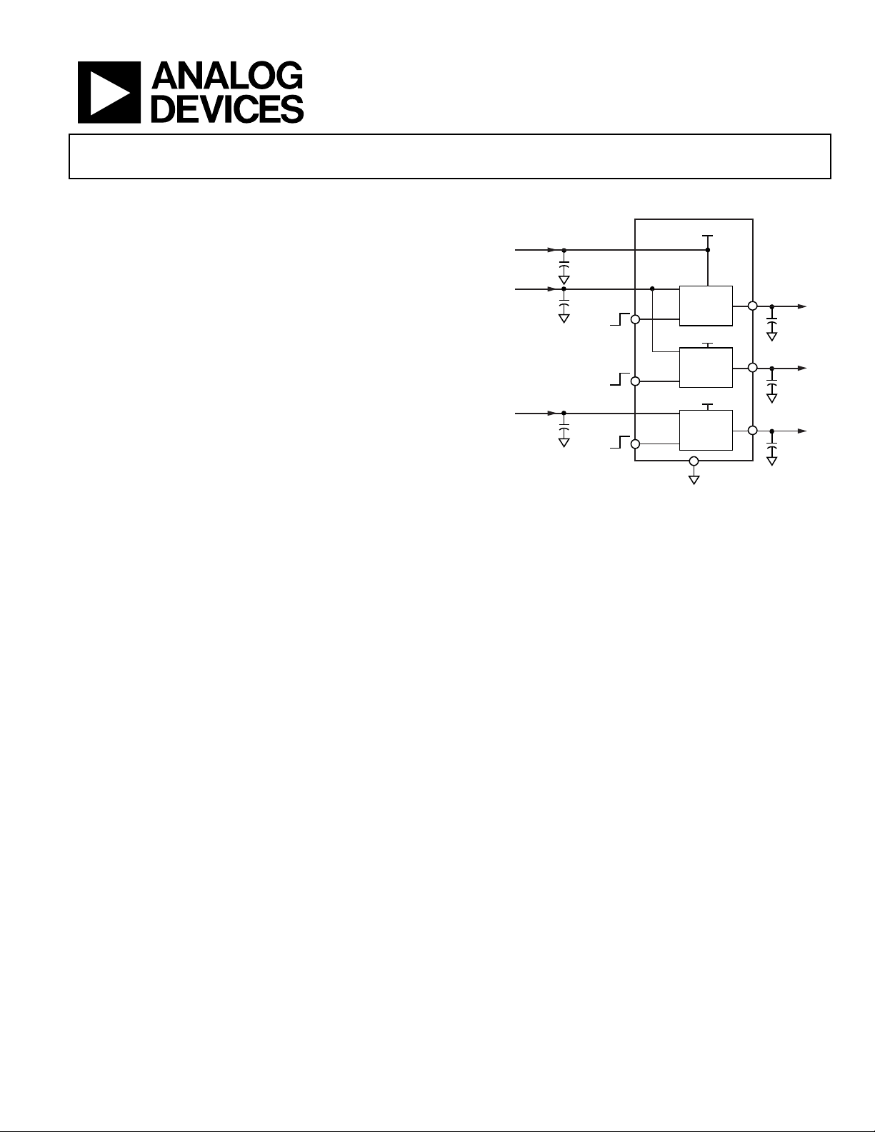
TYPICAL APPLICATION CIRCUITS
Figure 1. Typical Application Circuit
APPLICATIONS
Mobile phones
Digital cameras and audio devices
Portable and battery-powered equipment
Portable medical devices
Post dc-to-dc regulation
GENERAL DESCRIPTION
The ADP320 200 mA triple output LDO combines high PSRR, low
noise, low quiescent current, and low dropout voltage in a voltage
regulator ideally suited for wireless applications with demanding
performance and board space requirements.
The low quiescent current, low dropout voltage, and wide input
voltage range of the ADP320 triple LDO extend the battery life of
portable devices. The ADP320 triple LDO maintains power supply
rejection greater than 60 dB for frequencies as high as 100 kHz
while operating with a low headroom voltage. The ADP320 triple
Rev. A
Information furnished by Analog Devices is believed to be accurate and reliable. However, no
responsibility is assumed by Analog Devices for its use, nor for any infringements of patents or other
rights of third parties that may result from its use. Specifications subject to change without notice. No
license is granted by implication or otherwise under any patent or patent rights of Analog Devices.
Trademarks and registered trademarks are the property of their respective owners.
LDO offers much lower noise performance than competing LDOs
without the need for a noise bypass capacitor.
The ADP320 triple LDO is available in a miniature 16-lead
3 mm × 3 mm LFCSP package and is stable with tiny 1 µF ±30%
ceramic output capacitors, resulting in the smallest possible board
area for a wide variety of portable power needs.
The ADP320 triple LDO is available in output voltage combinations ranging from 0.8 V to 3.3 V and offers over current and
thermal protection to prevent damage in adverse conditions.
One Technology Way, P.O. Box 9106, Norwood, MA 02062-9106, U.S.A.
Tel: 781.329.4700
Fax: 781.461.3113 ©2010–2011 Analog Devices, Inc. All rights reserved.
www.analog.com
 Loading...