

Page 1
8-Bit Programmable 2- to 4-Phase
V
FEATURES
Selectable 2-, 3-, or 4-phase operation at up to
1 MHz per phase
±7.7 mV worst-case differential sensing error over
temperature
Logic-level PWM outputs for interface to external high
power drivers
Fast enhanced PWM (FEPWM) flex mode for excellent load
transient performance
Active current balancing between all output phases
Built-in power-good/crowbar blanking supports on-the-fly
VID code changes
Digitally programmable 0.5 V to 1.6 V output supports both
VR10.x and VR11 specifications
Programmable short-circuit protection with programmable
latch-off delay
APPLICATIONS
Desktop PC power supplies for next generation
Intel® processors
VRM modules
Synchronous Buck Controller
ADP3192A
FUNCTIONAL BLOCK DIAGRAM
CC RAMPADJRT
31 12 13
SHUNT
GND
PWRGD
TTSENSE
VRHOT
VRFAN
ILIMIT
DELAY
IREF
COMP
FBRTN
VIDSEL
REGULATOR
UVLO
SHUTDOWN
18
–
850mV
1
EN
2
10
9
8
11
7
20
5
3
40
+
DAC
+ 150mV
CSREF
+
–
DAC
– 350mV
DELAY
THERMAL
THROTTLING
CONTROL
PRECISION
REFERENCE
32
VID7
VID633VID534VID435VID336VID237VID138VID0
–
+
OSCILLATOR
VID DAC
+
CMP
–
+
CMP
–
CIRCUIT
CURRENT BALANCING
CURRENT
MEASUREMENT
AND LIMIT
–
+
Figure 1.
+
CMP
–
+
CMP
–
CROWBAR
+
–
SOFT START
CONTROL
39
ENSET
RESET
RESET
RESET
2/3/4-PHASE
DRIVER L OGIC
RESET
CURRENT
LIMIT
+
–
BOOT
VOLTAGE
AND
ADP3192A
19
30
29
28
27
25
24
23
22
17
15
16
21
4
14
6
OD
PWM1
PWM2
PWM3
PWM4
SW1
SW2
SW3
SW4
CSCOMP
CSREF
CSSUM
IMON
FB
LLSET
SS
06786-001
GENERAL DESCRIPTION
The ADP3192A1 is a highly efficient, multiphase, synchronous
buck-switching regulator controller optimized for converting a
12 V main supply into the core supply voltage required by high
performance Intel processors. It uses an internal 8-bit DAC to read
a voltage identification (VID) code directly from the processor,
which is used to set the output voltage between 0.5 V and 1.6 V.
This device uses a multimode PWM architecture to drive the
logic-level outputs at a programmable switching frequency that
can be optimized for VR size and efficiency. The phase relationship of the output signals can be programmed to provide 2-, 3-,
or 4-phase operation, allowing for the construction of up to
four complementary buck-switching stages.
1
Protected by U.S. Patent Number 6,683,441; other patents pending.
Rev. 0
Information furnished by Analog Devices is believed to be accurate and reliable. However, no
responsibility is assumed by Anal og Devices for its use, nor for any infringements of patents or ot her
rights of third parties that may result from its use. Specifications subject to change without notice. No
license is granted by implication or otherwise under any patent or patent rights of Analog Devices.
Trademarks and registered trademarks are the property of their respective owners.
The ADP3192A also includes programmable no load offset and
slope functions to adjust the output voltage as a function of the
load current, optimally positioning it for a system transient. In
addition, the ADP3192A provides accurate and reliable shortcircuit protection, adjustable current limiting, and a delayed
power-good output that accommodates on-the-fly output
voltage changes requested by the CPU.
The ADP3192A has a built-in shunt regulator that allows the part
to be connected to the 12 V system supply through a series resistor.
The ADP3192A is specified over the extended commercial
temperature range of 0°C to 85°C and is available in a
40-lead LFCSP.
One Technology Way, P.O. Box 9106, Norwood, MA 02062-9106, U.S.A.
Tel: 781.329.4700 www.analog.com
Fax: 781.461.3113 ©2007 Analog Devices, Inc. All rights reserved.
Page 2

ADP3192A
TABLE OF CONTENTS
Features.............................................................................................. 1
Applications....................................................................................... 1
Functional Block Diagram .............................................................. 1
General Description ......................................................................... 1
Revision History ............................................................................... 2
Specifications..................................................................................... 3
Test Circuits....................................................................................... 5
Absolute Maximum Ratings............................................................ 6
ESD Caution.................................................................................. 6
Pin Configuration and Function Descriptions............................. 7
Typical Performance Characteristics ............................................. 9
Theory of Operation ...................................................................... 10
Start-Up Sequence...................................................................... 10
Phase Detection Sequence......................................................... 10
Master Clock Frequency............................................................ 11
Output Voltage Differential Sensing ........................................ 11
Output Current Sensing ............................................................ 11
Active Impedance Control Mode............................................. 11
Current Control Mode and Thermal Balance ........................11
Voltage Control Mode................................................................ 12
Current Reference ......................................................................12
Fast Enhanced PWM Mode...................................................... 12
Delay Timer................................................................................. 12
Soft Start ...................................................................................... 12
Current-Limit, Short-Circuit, and Latch-Off Protection...... 13
Dynamic VID.............................................................................. 13
Power-Good Monitoring........................................................... 14
Output Crowbar......................................................................... 14
Output Enable and UVLO........................................................ 14
Thermal Monitoring.................................................................. 14
Application Information................................................................ 19
Setting the Clock Frequency..................................................... 19
Soft Start Delay Time................................................................. 19
Current-Limit Latch-Off Delay Times.................................... 19
Inductor Selection...................................................................... 19
Current Sense Amplifier............................................................ 20
Inductor DCR Temperature Correction ................................. 21
Output Offset.............................................................................. 22
C
Selection ............................................................................. 22
OUT
Power MOSFETs......................................................................... 23
Ramp Resistor Selection............................................................ 24
COMP Pin Ramp ....................................................................... 25
Current-Limit Setpoint.............................................................. 25
Feedback Loop Compensation Design.................................... 25
CIN Selection and Input Current di/dt Reduction.................. 27
Thermal Monitor Design .......................................................... 27
Shunt Resistor Design................................................................ 28
Tuning the ADP3192A .............................................................. 28
Layout and Component Placement ......................................... 30
Outline Dimensions....................................................................... 31
Ordering Guide .......................................................................... 31
REVISION HISTORY
5/07—Revision 0: Initial Version
Rev. 0 | Page 2 of 32
Page 3

ADP3192A
SPECIFICATIONS
VCC = 5 V, FBRTN = GND, TA = 0°C to 85°C, unless otherwise noted.
Table 1.
Parameter Symbol Conditions Min Typ Max Unit
REFERENCE CURRENT
Reference Bias Voltage V
Reference Bias Current I
1.5 V
IREF
R
IREF
= 100 kΩ 14.25 15 15.75 μA
IREF
ERROR AMPLIFIER
Output Voltage Range
Accuracy VFB
2
V
0 4.4 V
COMP
Relative to nominal DAC output, referenced
to FBRTN, LLSET = CSREF (see
V
In startup 1.092 1.1 1.108 V
FB(BOOT)
Load Line Positioning Accuracy CSREF − LLSET = 80 mV −78 −80 −82 mV
Differential Nonlinearity −1 +1 LSB
Input Bias Current IFB I
FBRTN Current I
Output Current I
Gain Bandwidth Product GBW
65 200 μA
FBRTN
COMP
(ERR)
= I
FB
FB forced to V
COMP = FB 20 MHz
Slew Rate COMP = FB 25 V/μs
LLSET Input Voltage Range V
LLSET Input Bias Current I
Boot Voltage Hold Time t
Relative to CSREF −250 +250 mV
LLSET
−10 +10 nA
LLSET
C
BOOT
DELAY
VID INPUTS
Input Low Voltage V
Input High Voltage V
Input Current I
VID Transition Delay Time
No CPU Detection Turn-Off Delay Time
2
2
VID(X), VIDSEL 0.4 V
IL(VID)
VID(X), VIDSEL 0.8 V
IH(VID)
−1 μA
IN(VID)
VID code change to FB change 400 ns
VID code change to PWM going low 5 μs
OSCILLATOR
Frequency Range
Frequency Variation f
T
T
Output Voltage VRT R
RAMPADJ Output Voltage V
RAMPADJ Input Current Range I
2
f
0.25 4 MHz
OSC
T
PHASE
RAMPADJ
RAMPADJ
= 25°C, RT = 205 kΩ, 4-phase 180 200 220 kHz
A
= 25°C, RT = 118 kΩ, 4-phase 400 kHz
A
= 25°C, RT = 55 kΩ, 4-phase 800 kHz
A
= 205 kΩ to GND 1.9 2.0 2.1 V
T
RAMPADJ − FB −50 +50 mV
1 50 μA
CURRENT SENSE AMPLIFIER
Offset Voltage V
Input Bias Current I
Gain Bandwidth Product GBW
Slew Rate C
CSSUM − CSREF (see Figure 3) −1.0 +1.0 mV
OS(CSA)
BIAS(CSSUM)
−10 +10 nA
CSSUM = CSCOMP 10 MHz
(CSA)
CSCOMP
Input Common-Mode Range CSSUM and CSREF 0 3.5 V
Output Voltage Range 0.05 3.5 V
Output Current I
Current Limit Latch-Off Delay Time t
500 μA
CSCOMP
C
OC(DELAY)
DELAY
IMON Output IMON 10 × (CSREF − CSCOMP) > 50 mV −6 +6 %
CURRENT BALANCE AMPLIFIER
Common-Mode Range V
Input Resistance R
Input Current I
Input Current Matching
SW(X)CM
SW(X)
SW(X)
ΔI
SW(X)
−600 +200 mV
SW(X) = 0 V 10 17 26 kΩ
SW(X) = 0 V 8 12 20 μA
SW(X) = 0 V −4 +4 %
CURRENT-LIMIT COMPARATOR
ILIMIT Bias Current I
I
ILIMIT
= 2/3 × I
ILIMIT
Rev. 0 | Page 3 of 32
1
−7.7 +7.7 mV
Figure 2)
13.5 15 16.5 μA
IREF
– 3% 500 μA
OUT
= 10 nF 2 ms
= 10 pF 10 V/μs
= 10 nF 8 ms
9 10 11 μA
IREF
Page 4

ADP3192A
Symbol Conditions Min Typ Max Unit Parameter
ILIMIT Voltage V
ILIMIT
Maximum Output Voltage 3 V
Current-Limit Threshold Voltage VCL V
Current-Limit Setting Ratio VCL/V
DELAY TIMER
Normal Mode Output Current I
Output Current in Current Limit I
Threshold Voltage V
DELAY
DELAY(CL)
DELAY(TH)
SOFT START
Output Current ISS During startup, ISS = I
ENABLE INPUT
Threshold Voltage V
Hysteresis V
Input Current I
Delay Time t
OD OUTPUT
Output Low Voltage V
Output High Voltage V
OD Pull-Down Resistor
TH(EN)
HYS(EN)
IN(EN)
DELAY(EN)
OL(OD)
OH(OD)
60 kΩ
THERMAL THROTTLING CONTROL
TTSENSE Voltage Range Internally limited 0 5 V
TTSENSE Bias Current −133 −123 −113 μA
TTSENSE VRFAN Threshold Voltage 1.06 1.105 1.15 V
TTSENSE VRHOT Threshold Voltage 765 810 855 mV
TTSENSE Hysteresis 50 mV
VRFAN Output Low Voltage V
VRHOT Output Low Voltage V
OL(VRFAN)
OL(VRHOT)
POWER-GOOD COMPARATOR
Undervoltage Threshold V
Overvoltage Threshold V
Output Low Voltage V
PWRGD(UV)
PWRGD(OV)
OL(PWRGD)
Power-Good Delay Time
During Soft Start
2
C
VID Code Changing 100 250 μs
VID Code Static 200 ns
Crowbar Trip Point V
CROWBAR
Crowbar Reset Point Relative to FBRTN 320 375 430 mV
Crowbar Delay Time t
CROWBAR
VID Code Changing 100 250 μs
VID Code Static 400 ns
PWM OUTPUTS
Output Low Voltage V
Output High Voltage V
OL(PWM)
OH(PWM)
SUPPLY V
2
VCC
DC Supply Current I
VCC 4.65 5 5.55 V
VCC
UVLO Turn-On Current 6.5 11 mA
UVLO Threshold Voltage V
UVLO
UVLO Turn-Off Voltage VCC falling 4.1 V
1
All limits at temperature extremes are guaranteed via correlation using standard statistical quality control (SQC).
2
Guaranteed by design or bench characterization, not tested in production.
R
ILIMIT
CSREF
I
DELAY
I
DELAY(CL)
= 121 kΩ (V
− V
CSCOMP
82.6 mV/V
ILIMIT
= I
12 15 18 μA
IREF
= 0.25 × I
= (I
× R
ILIMIT
ILIMIT
, R
= 121 kΩ 80 100 125 mV
ILIMIT
3.0 3.75 4.5 μA
IREF
)) 1.09 1.21 1.33 V
ILIMIT
1.6 1.7 1.8 V
12 15 18 μA
IREF
800 850 900 mV
80 100 125 mV
−1 μA
EN > 950 mV, C
= 10 nF 2 ms
DELAY
160 500 mV
4 5 V
I
I
= −4 mA 150 300 mV
VRFAN(SINK)
VRHOT(SINK)
= −4 mA 150 300 mV
Relative to nominal DAC output −400 −350 −300 mV
Relative to nominal DAC output 100 150 200 mV
I
PWRGD(SINK)
= −4 mA 150 300 mV
= 10 nF 2 ms
DELAY
Relative to nominal DAC output 100 150 200 mV
Overvoltage to PWM going low
I
I
= −400 μA 160 500 mV
PWM(SINK)
PWM(SOURCE)
SYSTEM
V
SYSTEM
= 400 μA 4.0 5 V
= 12 V, R
= 13.2 V, R
= 340 Ω (see Figure 2)
SHUNT
= 340 Ω 25 mA
SHUNT
VCC rising 9 V
Rev. 0 | Page 4 of 32
Page 5
ADP3192A
TEST CIRCUITS
12V
12V
ADP3192A
10nF
NC = NO CONNECT
8-BIT CODE
40
VCC
VID4
VID5
VID6
VID7
PWM1
PWM2
PWM3
PWM4
CSSUM
CSCOMP
GNDODIREF
100kΩ
20kΩ
1kΩ
1.25V
10nF
1
EN
PWRGD
FBRTN
FB
COMP
SS
DELAY
VRFAN
VRHOT
TTSENSE
250kΩ
VID0
VID1
VIDSEL
ADP3192A
ILIMITRTRAMPADJ
VID2
LLSET
VID3
CSREF
100nF
Figure 2. Closed-Loop Output Voltage Accuracy
12V
ADP3192A
680Ω 680Ω
VCC
31
+
SW1
SW2
SW3
SW4
680Ω680Ω
1µF
100nF
NC
NC
680Ω 680Ω
10kΩ
ΔV
1V
VCC
31
COMP
5
FB
4
LLSET
14
15
18
= FBΔV = 80mV – FBΔV = 0mV
ΔV
FB
–
CSREF
+
GND
VID
DAC
06786-004
Figure 4. Positioning Voltage
06786-002
CSCOMP
17
39kΩ
1kΩ
1V
100nF
CSSUM
16
CSREF
15
GND
18
VOS =
CSCOMP – 1V
Figure 3. Current Sense Amplifier V
40
06786-003
OS
Rev. 0 | Page 5 of 32
Page 6
ADP3192A
ABSOLUTE MAXIMUM RATINGS
Table 2.
Parameter Rating
VCC −0.3 V to +6 V
FBRTN −0.3 V to +0.3 V
PWM3 to PWM4, RAMPADJ −0.3 V to VCC + 0.3 V
SW1 to SW4 −5 V to +25 V
<200 ns −10 V to +25 V
All Other Inputs and Outputs −0.3 V to VCC + 0.3 V
Storage Temperature Range −65°C to +150°C
Operating Ambient Temperature Range 0°C to 85°C
Operating Junction Temperature 125°C
Thermal Impedance (θJA) 39°C/W
Lead Temperature
Soldering (10 sec) 300°C
Infrared (15 sec) 260°C
Stresses above those listed under Absolute Maximum Ratings
may cause permanent damage to the device. This is a stress
rating only; functional operation of the device at these or any
other conditions above those indicated in the operational
section of this specification is not implied. Exposure to absolute
maximum rating conditions for extended periods may affect
device reliability.
Absolute maximum ratings apply individually only, not in
combination. Unless otherwise specified, all other voltages
referenced to GND.
ESD CAUTION
Rev. 0 | Page 6 of 32
Page 7
ADP3192A
PIN CONFIGURATION AND FUNCTION DESCRIPTIONS
ID2
VID139VID040VIDSEL
38
PIN 1
1EN
INDICATOR
2PWRGD
3FBRTN
4FB
5COMP
6SS
7DELAY
8VRFAN
9VRHOT
10TTSENSE
NOTES
1. NC = NO CONNECT .
2. THE EXPO SED EPAD ON BOT TOM SI DE OF PACKAGE IS AN
ELECTRICAL CONNECTIO N AND SHOULD BE SOLDERED TO G ROUND.
ADP3192A
TOP VIEW
(Not to Scale)
11
12RT13
ILIMIT
RAMPADJ
Figure 5. Pin Configuration
VID634VID535VID436VID337V
VID731VCC
33
32
30 PWM1
29 PWM2
28 PWM3
27 PWM4
26 NC
25 SW1
24 SW2
23 SW3
22 SW4
21 IMON
15
17
16
18
14
LLSET
19OD20
ND
G
CSREF
IREF
CSSUM
CSCOMP
06786-005
Table 3. Pin Function Descriptions
Pin No. Mnemonic Description
1 EN Power Supply Enable Input. Pulling this pin to GND disables the PWM outputs and pulls the PWRGD output low.
2 PWRGD
Power-Good Output. Open-drain output that signals when the output voltage is outside of the proper
operating range.
3 FBRTN Feedback Return. VID DAC and error amplifier reference for remote sensing of the output voltage.
4 FB
Feedback Input. Error amplifier input for remote sensing of the output voltage. An external resistor between
this pin and the output voltage sets the no load offset point.
5 COMP Error Amplifier Output and Compensation Point.
6 SS
Soft Start Delay Setting Input. An external capacitor connected between this pin and GND sets the soft start
ramp-up time.
7 DELAY
Delay Timer Setting Input. An external capacitor connected between this pin and GND sets the overcurrent
latch-off delay time, boot voltage hold time, EN delay time, and PWRGD delay time.
8 VRFAN
VR Fan Activation Output. Open-drain output that signals when the temperature at the monitoring point
connected to TTSENSE exceeds the programmed VRFAN temperature threshold.
9 VRHOT
VR Hot Output. Open-drain output that signals when the temperature at the monitoring point connected to
TTSENSE exceeds the programmed VRHOT temperature threshold.
10 TTSENSE
VR Hot Thermal Throttling Sense Input. An NTC thermistor between this pin and GND is used to remotely sense
the temperature at the desired thermal monitoring point.
11 ILIMIT Current-Limit Setpoint. An external resistor from this pin to GND sets the current-limit threshold of the converter.
12 RT
Frequency Setting Resistor Input. An external resistor connected between this pin and GND sets the oscillator
frequency of the device.
13 RAMPADJ
PWM Ramp Current Input. An external resistor from the converter input voltage to this pin sets the internal
PWM ramp.
14 LLSET
Output Load Line Programming Input. This pin can be directly connected to CSCOMP, or it can be connected to
the center point of a resistor divider between CSCOMP and CSREF. Connecting LLSET to CSREF disables positioning.
15 CSREF
Current Sense Reference Voltage Input. The voltage on this pin is used as the reference for the current sense
amplifier and the power-good and crowbar functions. This pin should be connected to the common point of
the output inductors.
16 CSSUM
Current Sense Summing Node. External resistors from each switch node to this pin sum the average inductor
currents together to measure the total output current.
17 CSCOMP
Current Sense Compensation Point. A resistor and capacitor from this pin to CSSUM determines the gain of the
current sense amplifier and the positioning loop response time.
18 GND Ground. All internal biasing and the logic output signals of the device are referenced to this ground.
Rev. 0 | Page 7 of 32
Page 8

ADP3192A
Mnemonic Description Pin No.
19
20 IREF
21 IMON Analog Output. Represents the total load current.
22 to 25 SW4 to SW1
26 NC No Connection.
27 to 30 PWM4 to PWM1
31 VCC
32 to 39 VID7 to VID0
40 VIDSEL
OD Output Disable Logic Output. This pin is actively pulled low when the EN input is low or when VCC is below its
UVLO threshold to signal to the driver IC that the driver high-side and low-side outputs should go low.
, I
Current Reference Input. An external resistor from this pin to ground sets the reference current for I
I
ILIMIT
, and I
TTSENSE
.
, ISS,
FB
DELAY
Current Balance Inputs. Inputs for measuring the current level in each phase. The SW pins of unused phases
should be left open.
Logic-Level PWM Outputs. Each output is connected to the input of an external MOSFET driver such as the
ADP3120A. Connecting the PWM4 and PWM3 outputs to VCC causes that phase to turn off, allowing the
ADP3192A to operate as a 2-, 3-, or 4-phase controller.
Supply Voltage for the Device. A 340 Ω resistor should be placed between the 12 V system supply and the VCC
pin. The internal shunt regulator maintains VCC = 5 V.
Voltage Identification DAC Inputs. These eight pins are pulled down to GND, providing a Logic 0 if left open. When
in normal operation mode, the DAC output programs the FB regulation voltage from 0.5 V to 1.6 V (see
Table 4).
VID DAC Selection Pin. The logic state of this pin determines whether the internal VID DAC decodes VID0 to
VID7 as extended VR10 or VR11 inputs.
Rev. 0 | Page 8 of 32
Page 9
ADP3192A
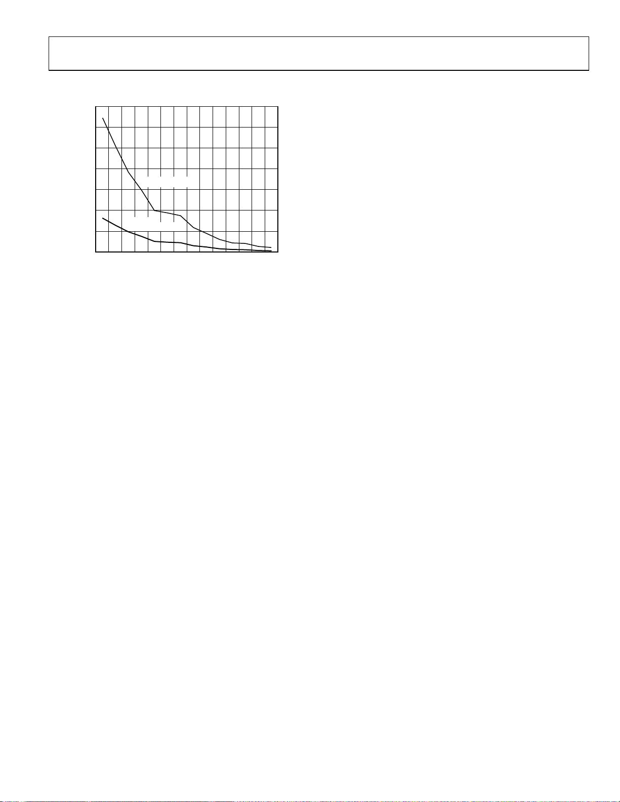
TYPICAL PERFORMANCE CHARACTERISTICS
7000
6000
5000
4000
3000
FREQUENCY (kHz)
2000
1000
MASTER CLOCK
PHASE 1
IN 4 PHASE DESIGN
0
13
20 30 43 68 75 82 130 180 270 395 430 680 850
RT (kΩ)
06786-018
Figure 6. Master Clock Frequency vs. RT
Rev. 0 | Page 9 of 32
Page 10
ADP3192A
THEORY OF OPERATION
The ADP3192A combines a multimode, fixed frequency,
PWM control with multiphase logic outputs for use in 2-, 3-,
and 4-phase synchronous buck CPU core supply power
converters. The internal VID DAC is designed to interface
with the Intel 8-bit VRD/VRM 11-compatible CPU and 7-bit
VRD/VRM 10×-compatible CPU. Multiphase operation is
important for producing the high currents and low voltages
demanded by today’s microprocessors. Handling the high
currents in a single-phase converter places high thermal
demands on the components in the system, such as the
inductors and MOSFETs.
The multimode control of the ADP3192A ensures a stable,
high performance topology for the following:
• Balancing currents and thermals between phases
• High speed response at the lowest possible switching
frequency and output decoupling
• Minimizing thermal switching losses by using lower
frequency operation
• Tight load line regulation and accuracy
• High current output due to 4-phase operation
• Reduced output ripple due to multiphase cancellation
• PC board layout noise immunity
• Ease of use and design due to independent component
selection
• Flexibility in operation for tailoring design to low cost or
high performance
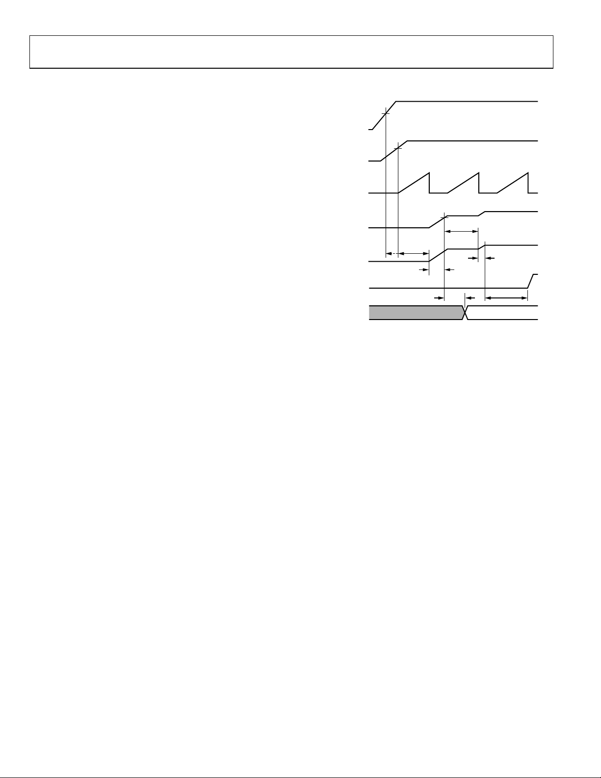
START-UP SEQUENCE
The ADP3192A follows the VR11 start-up sequence shown in
Figure 7. After both the EN and UVLO conditions are met,
the DELAY pin goes through one cycle (TD1). The first four
clock cycles of TD2 are blanked from the PWM outputs and
used for phase detection as explained in the
Sequence
section. Then, the soft start ramp is enabled (TD2),
and the output comes up to the boot voltage of 1.1 V. The boot
hold time is determined by the DELAY pin as it goes through a
second cycle (TD3). During TD3, the processor VID pins settle
to the required VID code. When TD3 is over, the ADP3192A
soft starts either up or down to the final VID voltage (TD4).
After TD4 is complete and the PWRGD masking time (equal to
VID on-the-fly masking) is complete, a third ramp on the
DELAY pin sets the PWRGD blanking (TD5).
Phase Detection
(ADP3192A EN)
(ADP3192A PWRGD)
PHASE DETECTION SEQUENCE
During startup, the number of operational phases and their
phase relationship is determined by the internal circuitry that
monitors the PWM outputs. Normally, the ADP3192A operates
as a 4-phase PWM controller. Connecting the PWM4 pin to
VCC programs 3-phase operation and connecting the PWM4
and PWM3 pins to VCC programs 2-phase operation.
Prior to soft start, while EN is low, the PWM3 and PWM4 pins
sink approximately 100 µA. An internal comparator checks each
pin’s voltage vs. a threshold of 3 V. If the pin is tied to VCC, it is
above the threshold. Otherwise, an internal current sink pulls
the pin to GND, which is below the threshold. PWM1 and
PWM2 are low during the phase detection interval that occurs
during the first four clock cycles of TD2. After this time, if the
remaining PWM outputs are not pulled to VCC, the 100 µA
current sink is removed, and they function as normal PWM
outputs. If they are pulled to VCC, the 100 µA current source is
removed, and the outputs are put into a high impedance state.
The PWM outputs are logic-level devices intended for driving
external gate drivers such as the
phase is monitored independently, operation approaching 100%
duty cycle is possible. In addition, more than one output can be
on at the same time to allow overlapping phases.
SUPPLY
VTT I/O
DELAY
VCC_CORE
VR READY
CPU
VID INPUTS
5V
SS
UVLO
THRESHOLD
0.85V
V
DELAY(TH)
(1.7V)
1V
TD1
TD2
50µs
VID INVALID VID VALID
Figure 7. System Start-Up Sequence
ADP3120A. Because each
V
BOOT
(1.1V)
TD3
V
BOOT
(1.1V)
V
VID
V
VID
TD4
TD5
06786-006
Rev. 0 | Page 10 of 32
Page 11

ADP3192A
MASTER CLOCK FREQUENCY
The clock frequency of the ADP3192A is set with an external
resistor connected from the RT pin to GND. The frequency
follows the graph in
phase, the clock is divided by the number of phases in use. If all
phases are in use, divide by 4. If PWM4 is tied to VCC, divide
the master clock by 3 for the frequency of the remaining phases.
If PWM3 and PWM4 are tied to VCC, divide by 2.
Figure 6. To determine the frequency per
OUTPUT VOLTAGE DIFFERENTIAL SENSING
The ADP3192A combines differential sensing with a high
accuracy VID DAC and reference, and a low offset error amplifier. This maintains a worst-case specification of ±7.7 mV
differential sensing error over its full operating output voltage
and temperature range. The output voltage is sensed between
the FB pin and FBRTN pin. FB should be connected through
a resistor to the regulation point, usually the remote sense pin
of the microprocessor. FBRTN should be connected directly
to the remote sense ground point. The internal VID DAC
and precision reference are referenced to FBRTN, which has a
minimal current of 65 µA to allow accurate remote sensing. The
internal error amplifier compares the output of the DAC to the
FB pin to regulate the output voltage.
OUTPUT CURRENT SENSING
The ADP3192A provides a dedicated current-sense amplifier
(CSA) to monitor the total output current for proper voltage
positioning vs. load current and for current-limit detection.
Sensing the load current at the output gives the total average
current being delivered to the load. This is an inherently more
accurate method than peak current detection or sampling the
current across a sense element such as the low-side MOSFET.
This amplifier can be configured several ways, depending on
the objectives of the system, as follows:
• Output inductor DCR sensing without a thermistor for
lowest cost
• Output inductor DCR sensing with a thermistor for
improved accuracy with tracking of inductor temperature
• Sense resistors for highest accuracy measurements
The positive input of the CSA is connected to the CSREF pin,
which is connected to the output voltage. The inputs to the
amplifier are summed together through resistors from the sensing
element, such as the switch node side of the output inductors,
to the inverting input CSSUM. The feedback resistor between
CSCOMP and CSSUM sets the gain of the amplifier and a filter
capacitor is placed in parallel with this resistor. The gain of the
amplifier is programmable by adjusting the feedback resistor.
An additional resistor divider connected between CSREF and
CSCOMP (with the midpoint connected to LLSET) can be used
to set the load line required by the microprocessor. The current
information is then given as CSREF − LLSET. This difference
signal is used internally to offset the VID DAC for voltage
positioning. The difference between CSREF and CSCOMP is
then used as a differential input for the current-limit comparator.
This allows the load line to be set independently of the currentlimit threshold. In the event that the current-limit threshold
and load line are not independent, the resistor divider between
CSREF and CSCOMP can be removed, and the CSCOMP pin
can be directly connected to LLSET. To disable voltage positioning entirely (that is, no load line), connect LLSET to CSREF.
To provide the best accuracy for sensing current, the CSA is
designed to have a low offset input voltage. Also, the sensing gain
is determined by external resistors to make it extremely accurate.
ACTIVE IMPEDANCE CONTROL MODE
For controlling the dynamic output voltage droop as a function
of output current, a signal proportional to the total output current
at the LLSET pin can be scaled to equal the regulator droop
impedance multiplied by the output current. This droop voltage
is then used to set the input control voltage to the system. The
droop voltage is subtracted from the DAC reference input
voltage to tell the error amplifier where the output voltage
should be. This allows enhanced feed-forward response.
CURRENT CONTROL MODE AND THERMAL BALANCE
The ADP3192A has individual inputs (SW1 to SW4) for each
phase that are used for monitoring the current of each phase.
This information is combined with an internal ramp to create
a current balancing feedback system that has been optimized for
initial current balance accuracy and dynamic thermal balancing
during operation. This current balance information is independent
of the average output current information used for positioning
as described in the
The magnitude of the internal ramp can be set to optimize the
transient response of the system. It also monitors the supply
voltage for feed-forward control for changes in the supply. A
resistor connected from the power input voltage to the RAMPADJ
pin determines the slope of the internal PWM ramp. External
resistors can be placed in series with individual phases to create
an intentional current imbalance if desired, such as when one
phase has better cooling and can support higher currents.
Resistor R
for adjusting thermal balance in this 4-phase example. It is best
to have the ability to add these resistors during the initial design;
therefore, ensure that placeholders are provided in the layout.
SW1
Output Current Sensing section.
through Resistor R
(see Figure 10) can be used
SW4
Rev. 0 | Page 11 of 32
Page 12

ADP3192A
To increase the current in any given phase, enlarge RSW for that
phase (make R
during balancing). Increasing R
tial increase in phase current. Increase each R
amounts to achieve balance, starting with the coolest phase first.
VOLTAGE CONTROL MODE
A high gain, high bandwidth, voltage mode error amplifier is
used for the voltage mode control loop. The control input voltage
to the positive input is set via the VID logic according to the
voltages listed in
This voltage is also offset by the droop voltage for active
positioning of the output voltage as a function of current,
commonly known as active voltage positioning. The output
of the amplifier is the COMP pin, which sets the termination
voltage for the internal PWM ramps.
The negative input (FB) is tied to the output sense location with
Resistor R
voltage at this point. A current source (equal to IREF) from the
FB pin flowing through R
voltage from the VID voltage. The no load voltage is negative
with respect to the VID DAC. The main loop compensation is
incorporated into the feedback network between FB and COMP.
CURRENT REFERENCE
The IREF pin is used to set an internal current reference. This
reference current sets I
to ground programs the current based on the 1.5 V output.
IREF
Ty pi ca ll y,
following currents are then equal to
IFB = IREF = 15 µA
I
DELAY
I
= IREF = 15 µA
SS
I
LIMIT
= 0 for the hottest phase and do not change it
SW
to only 500 Ω makes a substan-
SW
value by small
SW
Tabl e 4.
and is used for sensing and controlling the output
B
is used for setting the no load offset
B
, I
DELAY
, ISS, I
FB
V5.1
=
R
IREF
R
IREF
is set to 100 kΩ to program IREF = 15 µA. The
LIMIT
, and I
TTSENSE
. A resistor
= IREF = 15 µA
= 2/3 (IREF) = 10 µA
FAST ENHANCED PWM MODE
Fast enhanced PWM mode (FEPWM) is intended to improve
the transient response of the ADP3192A to a load setup. In
previous generations of controllers, when a load step-up
occurred, the controller had to wait until the next turn-on of
the PWM signal to respond to the load change. Enhanced
PWM mode allows the controller to immediately respond when
a load step-up occurs. This allows the phases to respond more
quickly when a load increase takes place.
DELAY TIMER
The delay times for the start-up timing sequence are set with a
capacitor from the DELAY pin to GND. In UVLO, or when EN is
logic low, the DELAY pin is held at GND. After the UVLO and
EN signals are asserted, the first delay time (TD1 in
initiated. A current flows out of the DELAY pin to charge C
Figure 7) is
DLY
.
This current is equal to IREF, which is typically 15 µA. A comparator monitors the DELAY voltage with a threshold of 1.7 V. The
delay time is therefore set by the IREF current charging a capacitor
from 0 V to 1.7 V. This DELAY pin is used for multiple delay
timings (TD1, TD3, and TD5) during the start-up sequence. In
addition, DELAY is used for timing the current-limit latch off,
as explained in the
Protection
section.
Current-Limit, Short-Circuit, and Latch-Off
SOFT START
The soft start times for the output voltage are set with a
capacitor from the SS pin to GND. After TD1 and the phase
detection cycle are complete, the SS time (TD2 in
starts. The SS pin is disconnected from GND, and the capacitor
is charged up to the 1.1 V boot voltage by the SS amplifier,
which has an output current equal to IREF (typically 15 µA).
The voltage at the FB pin follows the ramping voltage on the
SS pin, limiting the inrush current during startup. The soft start
time depends on the value of the boot voltage and C
Once the SS voltage is within 100 mV of the boot voltage, the
boot voltage delay time (TD3 in
Figure 7) is started. The end of
the boot voltage delay time signals the beginning of the second
soft start time (TD4 in
Figure 7). The SS voltage now changes
from the boot voltage to the programmed VID DAC voltage
(either higher or lower) using the SS amplifier with the output
current equal to IREF. The voltage of the FB pin follows the
ramping voltage of the SS pin, limiting the inrush current
during the transition from the boot voltage to the final DAC
voltage. The second soft start time depends on the boot voltage,
the programmed VID DAC voltage, and C
SS
.
Figure 7)
.
SS
Rev. 0 | Page 12 of 32
Page 13

ADP3192A
If EN is taken low or if VCC drops below UVLO, DELAY and
SS are reset to ground to be ready for another soft start cycle.
Figure 8 shows typical start-up waveforms for the ADP3192A.
1
2
3
4
CH1 1V CH2 1V
CH4 10VCH3 1V
Figure 8. Typical Start-Up Waveforms
(Channel 1: CSREF, Channel 2: DELAY,
Channel 3: SS, Channel 4: Phase 1 Switch Node)
M 1ms A CH1 700mV
T 40.4%
06786-007
CURRENT-LIMIT, SHORT-CIRCUIT, AND LATCHOFF PROTECTION
The ADP3192A compares a programmable current-limit
setpoint to the voltage from the output of the current-sense
amplifier. The level of current limit is set with the resistor
from the ILIMIT pin to GND. During operation, the current
from ILIMIT is equal to 2/3 of IREF, giving 10 µA typically.
This current through the external resistor sets the ILIMIT
voltage, which is internally scaled to give a current-limit
threshold of 82.6 mV/V. If the difference in voltage between
CSREF and CSCOMP rises above the current-limit threshold,
the internal current-limit amplifier controls the internal COMP
voltage to maintain the average output current at the limit.
If the limit is reached and TD5 in
off delay time starts, and the controller shuts down if the fault is
not removed. The current-limit delay time shares the
DELAY pin timing capacitor with the start-up sequence timing.
However, during current limit, the DELAY pin current is
reduced to IREF/4. A comparator monitors the DELAY voltage
and shuts off the controller when the voltage reaches 1.7 V.
Therefore, the current-limit latch-off delay time is set by the
current of IREF/4 charging the delay capacitor from 0 V to 1.7 V.
This delay is four times longer than the delay time during the
start-up sequence.
The current-limit delay time starts only after the TD5 is
complete. If there is a current limit during startup, the
ADP3192A goes through TD1 to TD5, and then starts the
latch-off time. Because the controller continues to cycle the
phases during the latch-off delay time, the controller returns to
normal operation and the DELAY capacitor is reset to GND if
the short is removed before the 1.7 V threshold is reached.
Figure 7 is complete, a latch-
The latch-off function can be reset by either removing and
reapplying the supply voltage to the ADP3192A or by toggling
the EN pin low for a short time. To disable the short-circuit
latch-off function, an external resistor should be placed in
parallel with C
. This prevents the DELAY capacitor from
DLY
charging up to the 1.7 V threshold. The addition of this resistor
causes a slight increase in the delay times.
During startup, when the output voltage is below 200 mV,
a secondary current limit is active. This is necessary because
the voltage swing of CSCOMP cannot go below GND. This
secondary current limit controls the internal COMP voltage
to the PWM comparators to 1.5 V. This limits the voltage drop
across the low-side MOSFETs through the current balance
circuitry. An inherent per-phase current limit protects
individual phases if one or more phases stop functioning
because of a faulty component. This limit is based on the
maximum normal mode COMP voltage. Typical overcurrent
latch-off waveforms are shown in
1
2
3
4
CH1 1V CH2 1V
CH4 10VCH3 2V
Figure 9. Overcurrent Latch-Off Waveforms
(Channel 1: CSREF, Channel 2: DELAY,
Channel 3: COMP, Channel 4: Phase 1 Switch Node)
Figure 9.
M 2ms A CH1 680mV
T 61.8%
06786-008
DYNAMIC VID
The ADP3192A has the ability to dynamically change the VID
inputs while the controller is running. This allows the output
voltage to change while the supply is running and supplying
current to the load, which is commonly referred to as VID onthe-fly (OTF). A VID OTF can occur under light or heavy load
conditions. The processor signals the controller by changing the
VID inputs in multiple steps from the start code to the finish
code. This change can be positive or negative.
When a VID input changes state, the ADP3192A detects the
change and ignores the DAC inputs for a minimum of 400 ns.
This time prevents a false code due to logic skew while the eight
VID inputs are changing. Additionally, the first VID change
initiates the PWRGD and crowbar blanking functions for a
minimum of 100 µs to prevent a false PWRGD or crowbar
event. Each VID change resets the internal timer.
Rev. 0 | Page 13 of 32
Page 14

ADP3192A
POWER-GOOD MONITORING
The power-good comparator monitors the output voltage via
the CSREF pin. The PWRGD pin is an open-drain output whose
high level, when connected to a pull-up resistor, indicates that
the output voltage is within the specified nominal limits based
on the VID voltage setting. PWRGD goes low if the output
voltage is outside of this specified range, if the VID DAC inputs
are in no CPU mode, or if the EN pin is pulled low. PWRGD is
blanked during a VID OTF event for a period of 200 µs to
prevent false signals during the time the output is changing.
The PWRGD circuitry also incorporates an initial turn-on
delay time (TD5) based on the DELAY timer. Prior to the
SS voltage reaching the programmed VID DAC voltage and the
PWRGD masking-time finishing, the PWRGD pin is held low.
Once the SS pin is within 100 mV of the programmed DAC
voltage, the capacitor on the DELAY pin begins to charge.
A comparator monitors the DELAY voltage and enables
PWRGD when the voltage reaches 1.7 V. The PWRGD delay
time is set, therefore, by a current of IREF, charging a capacitor
from 0 V to 1.7 V.
OUTPUT CROWBAR
To protect the load and output components of the supply, the
PWM outputs are driven low, which turns on the low-side
MOSFETs when the output voltage exceeds the upper crowbar
threshold. This crowbar action stops once the output voltage
falls below the release threshold of approximately 375 mV.
Turning on the low-side MOSFETs pulls down the output as
the reverse current builds up in the inductors. If the output
overvoltage is due to a short in the high-side MOSFET, this
action current limits the input supply or blows its fuse,
protecting the microprocessor from being destroyed.
OUTPUT ENABLE AND UVLO
For the ADP3192A to begin switching, the input supply (VCC)
to the controller must be higher than the UVLO threshold and
the EN pin must be higher than its 0.85 V threshold. This
initiates a system start-up sequence. If either UVLO or EN is
less than their respective thresholds, the ADP3192A is disabled.
This holds the PWM outputs at ground, shorts the DELAY
capacitor to ground, and forces PWRGD and
In the application circuit (see
connected to the
Grounding
DRVL are grounded. This feature is important in preventing the
discharge of the output capacitors when the controller is shut
off. If the driver outputs are not disabled, a negative voltage can
be generated during output due to the high current discharge of
the output capacitors through the inductors.
OD
inputs of the ADP3120A drivers.
OD
disables the drivers such that both DRVH and
Figure 10), the OD pin should be
OD
signals low.
THERMAL MONITORING
The ADP3192A includes a thermal monitoring circuit to detect
when a point on the VR has exceeded two different user-defined
temperatures. The thermal monitoring circuit requires an NTC
thermistor to be placed between TTSENSE and GND.
A fixed current of 8 × IREF (typically giving 123 µA) is sourced
out of the TTSENSE pin and into the thermistor. The current
source is internally limited to 5 V. An internal circuit compares
the TTSENSE voltage to a 1.105 V and a 0.81 V threshold, and
outputs an open-drain signal at the VRFAN and VRHOT
outputs, respectively. Once the voltage on the TTSENSE pin
drops below its respective threshold, the open-drain outputs
assert high to signal the system that an overtemperature event
has occurred. Because the TTSENSE voltage changes slowly
with respect to time, 50 mV of hysteresis is built into these comparators. The thermal monitoring circuitry does not depend on
EN and is active when UVLO is above its threshold. When UVLO
is below its threshold, VRFAN and VRHOT are forced low.
Table 4.VR11 and VR10.x VID Codes for the ADP3192A
VR11 DAC CODES: VIDSEL = HIGH VR10.x DAC CODES: VIDSEL = LOW
OUTPUT VID7 VID6 VID5 VID4 VID3 VID2 VID1 VID0 VID4 VID3 VID2 VID1 VID0 VID5 VID6
OFF 0 0 0 0 0 0 0 0 N/A
OFF 0 0 0 0 0 0 0 1 N/A
1.60000 0 0 0 0 0 0100101 0 11
1.59375 0 0 0 0 0 0110101 0 10
1.58750 0 0 0 0 0 1000101 1 01
1.58125 0 0 0 0 0 1010101 1 00
1.57500 0 0 0 0 0 1100101 1 11
1.56875 0 0 0 0 0 1110101 1 10
1.56250 0 0 0 0 1 0000110 0 01
1.55625 0 0 0 0 1 0010110 0 00
1.55000 0 0 0 0 1 0100110 0 11
1.54375 0 0 0 0 1 0110110 0 10
1.53750 0 0 0 0 1 1000110 1 01
1.53125 0 0 0 0 1 1010110 1 00
1.52500 0 0 0 0 1 1100110 1 11
1.51875 0 0 0 0 1 1110110 1 10
Rev. 0 | Page 14 of 32
Page 15

ADP3192A
VR11 DAC CODES: VIDSEL = HIGH VR10.x DAC CODES: VIDSEL = LOW
OUTPUT VID7 VID6 VID5 VID4 VID3 VID2 VID1 VID0 VID4 VID3 VID2 VID1 VID0 VID5 VID6
1.51250 0 0 0 1 0 000011 1 001
1.50625 0 0 0 1 0 001011 1 000
1.50000 0 0 0 1 0 010011 1 011
1.49375 0 0 0 1 0 011011 1 010
1.48750 0 0 0 1 0 100011 1 101
1.48125 0 0 0 1 0 101011 1 100
1.47500 0 0 0 1 0 110011 1 111
1.46875 0 0 0 1 0 111011 1 110
1.46250 0 0 0 1 1 000100 0 001
1.45625 0 0 0 1 1 001100 0 000
1.45000 0 0 0 1 1 010100 0 011
1.44375 0 0 0 1 1 011100 0 010
1.43750 0 0 0 1 1 100100 0 101
1.43125 0 0 0 1 1 101100 0 100
1.42500 0 0 0 1 1 110100 0 111
1.41875 0 0 0 1 1 111100 0 110
1.41250 0 0 1 0 0 000100 1 001
1.40625 0 0 1 0 0 001100 1 000
1.40000 0 0 1 0 0 010100 1 011
1.39375 0 0 1 0 0 011100 1 010
1.38750 0 0 1 0 0 100100 1 101
1.38125 0 0 1 0 0 101100 1 100
1.37500 0 0 1 0 0 110100 1 111
1.36875 0 0 1 0 0 111100 1 110
1.36250 0 0 1 0 1 000101 0 001
1.35625 0 0 1 0 1 001101 0 000
1.35000 0 0 1 0 1 010101 0 011
1.34375 0 0 1 0 1 011101 0 010
1.33750 0 0 1 0 1 100101 0 101
1.33125 0 0 1 0 1 101101 0 100
1.32500 0 0 1 0 1 110101 0 111
1.31875 0 0 1 0 1 111101 0 110
1.31250 0 0 1 1 0 000101 1 001
1.30625 0 0 1 1 0 001101 1 000
1.30000 0 0 1 1 0 010101 1 011
1.29375 0 0 1 1 0 011101 1 010
1.28750 0 0 1 1 0 100101 1 101
1.28125 0 0 1 1 0 101101 1 100
1.27500 0 0 1 1 0 110101 1 111
1.26875 0 0 1 1 0 111101 1 110
1.26250 0 0 1 1 1 000110 0 001
1.25625 0 0 1 1 1 001110 0 000
1.25000 0 0 1 1 1 010110 0 011
1.24375 0 0 1 1 1 011110 0 010
1.23750 0 0 1 1 1 100110 0 101
1.23125 0 0 1 1 1 101110 0 100
1.22500 0 0 1 1 1 110110 0 111
1.21875 0 0 1 1 1 111110 0 110
1.21250 0 1 0 0 0 000110 1 001
1.20625 0 1 0 0 0 001110 1 000
1.20000 0 1 0 0 0 010110 1 011
1.19375 0 1 0 0 0 011110 1 010
1.18750 0 1 0 0 0 100110 1 101
1.18125 0 1 0 0 0 101110 1 100
1.17500 0 1 0 0 0 110110 1 111
1.16875 0 1 0 0 0 111110 1 110
1.16250 0 1 0 0 1 000111 0 001
1.15625 0 1 0 0 1 001111 0 000
1.15000 0 1 0 0 1 010111 0 011
Rev. 0 | Page 15 of 32
Page 16

ADP3192A
VR11 DAC CODES: VIDSEL = HIGH VR10.x DAC CODES: VIDSEL = LOW
OUTPUT VID7 VID6 VID5 VID4 VID3 VID2 VID1 VID0 VID4 VID3 VID2 VID1 VID0 VID5 VID6
1.14375 0 1 0 0 1 0111110 0 10
1.13750 0 1 0 0 1 1001110 1 01
1.13125 0 1 0 0 1 1011110 1 00
1.12500 0 1 0 0 1 1101110 1 11
1.11875 0 1 0 0 1 1111110 1 10
1.11250 0 1 0 1 0 0001111 0 01
1.10625 0 1 0 1 0 0011111 0 00
1.10000 0 1 0 1 0 0101111 0 11
1.09375 0 1 0 1 0 0111111 0 10
OFF N/A 1111 1 01
OFF N/A 1111 1 00
OFF N/A 1111 1 11
OFF N/A 1111 1 10
1.08750 0 1 0 1 0 1000000 0 01
1.08125 0 1 0 1 0 1010000 0 00
1.07500 0 1 0 1 0 1100000 0 11
1.06875 0 1 0 1 0 1110000 0 10
1.06250 0 1 0 1 1 0000000 1 01
1.05625 0 1 0 1 1 0010000 1 00
1.05000 0 1 0 1 1 0100000 1 11
1.04375 0 1 0 1 1 0110000 1 10
1.03750 0 1 0 1 1 1000001 0 01
1.03125 0 1 0 1 1 1010001 0 00
1.02500 0 1 0 1 1 1100001 0 11
1.01875 0 1 0 1 1 1110001 0 10
1.01250 0 1 1 0 0 0000001 1 01
1.00625 0 1 1 0 0 0010001 1 00
1.00000 0 1 1 0 0 0100001 1 11
0.99375 0 1 1 0 0 0110001 1 10
0.98750 0 1 1 0 0 1000010 0 01
0.98125 0 1 1 0 0 1010010 0 00
0.97500 0 1 1 0 0 1100010 0 11
0.96875 0 1 1 0 0 1110010 0 10
0.96250 0 1 1 0 1 0000010 1 01
0.95625 0 1 1 0 1 0010010 1 00
0.95000 0 1 1 0 1 0100010 1 11
0.94375 0 1 1 0 1 0110010 1 10
0.93750 0 1 1 0 1 1000011 0 01
0.93125 0 1 1 0 1 1010011 0 00
0.92500 0 1 1 0 1 1100011 0 11
0.91875 0 1 1 0 1 1110011 0 10
0.91250 0 1 1 1 0 0000011 1 01
0.90625 0 1 1 1 0 0010011 1 00
0.90000 0 1 1 1 0 0100011 1 11
0.89375 0 1 1 1 0 0110011 1 10
0.88750 0 1 1 1 0 1000100 0 01
0.88125 0 1 1 1 0 1010100 0 00
0.87500 0 1 1 1 0 1100100 0 11
0.86875 0 1 1 1 0 1110100 0 10
0.86250 0 1 1 1 1 0000100 1 01
0.85625 0 1 1 1 1 0010100 1 00
0.85000 0 1 1 1 1 0100100 1 11
0.84375 0 1 1 1 1 0110100 1 10
0.83750 0 1 1 1 1 1000101 0 01
0.83125 0 1 1 1 1 1010101 0 00
0.82500 0 1 1 1 1 1 1 0 N/A
0.81875 0 1 1 1 1 1 1 1 N/A
0.81250 1 0 0 0 0 0 0 0 N/A
0.80625 1 0 0 0 0 0 0 1 N/A
Rev. 0 | Page 16 of 32
Page 17

ADP3192A
VR11 DAC CODES: VIDSEL = HIGH VR10.x DAC CODES: VIDSEL = LOW
OUTPUT VID7 VID6 VID5 VID4 VID3 VID2 VID1 VID0 VID4 VID3 VID2 VID1 VID0 VID5 VID6
0.80000 1 0 0 0 0 0 1 0 N/A
0.79375 1 0 0 0 0 0 1 1 N/A
0.78750 1 0 0 0 0 1 0 0 N/A
0.78125 1 0 0 0 0 1 0 1 N/A
0.77500 1 0 0 0 0 1 1 0 N/A
0.76875 1 0 0 0 0 1 1 1 N/A
0.76250 1 0 0 0 1 0 0 0 N/A
0.75625 1 0 0 0 1 0 0 1 N/A
0.75000 1 0 0 0 1 0 1 0 N/A
0.74375 1 0 0 0 1 0 1 1 N/A
0.73750 1 0 0 0 1 1 0 0 N/A
0.73125 1 0 0 0 1 1 0 1 N/A
0.72500 1 0 0 0 1 1 1 0 N/A
0.71875 1 0 0 0 1 1 1 1 N/A
0.71250 1 0 0 1 0 0 0 0 N/A
0.70625 1 0 0 1 0 0 0 1 N/A
0.70000 1 0 0 1 0 0 1 0 N/A
0.69375 1 0 0 1 0 0 1 1 N/A
0.68750 1 0 0 1 0 1 0 0 N/A
0.68125 1 0 0 1 0 1 0 1 N/A
0.67500 1 0 0 1 0 1 1 0 N/A
0.66875 1 0 0 1 0 1 1 1 N/A
0.66250 1 0 0 1 1 0 0 0 N/A
0.65625 1 0 0 1 1 0 0 1 N/A
0.65000 1 0 0 1 1 0 1 0 N/A
0.64375 1 0 0 1 1 0 1 1 N/A
0.63750 1 0 0 1 1 1 0 0 N/A
0.63125 1 0 0 1 1 1 0 1 N/A
0.62500 1 0 0 1 1 1 1 0 N/A
0.61875 1 0 0 1 1 1 1 1 N/A
0.61250 1 0 1 0 0 0 0 0 N/A
0.60625 1 0 1 0 0 0 0 1 N/A
0.60000 1 0 1 0 0 0 1 0 N/A
0.59375 1 0 1 0 0 0 1 1 N/A
0.58750 1 0 1 0 0 1 0 0 N/A
0.58125 1 0 1 0 0 1 0 1 N/A
0.57500 1 0 1 0 0 1 1 0 N/A
0.56875 1 0 1 0 0 1 1 1 N/A
0.56250 1 0 1 0 1 0 0 0 N/A
0.55625 1 0 1 0 1 0 0 1 N/A
0.55000 1 0 1 0 1 0 1 0 N/A
0.54375 1 0 1 0 1 0 1 1 N/A
0.53750 1 0 1 0 1 1 0 0 N/A
0.53125 1 0 1 0 1 1 0 1 N/A
0.52500 1 0 1 0 1 1 1 0 N/A
0.51875 1 0 1 0 1 1 1 1 N/A
0.51250 1 0 1 1 0 0 0 0 N/A
0.50625 1 0 1 1 0 0 0 1 N/A
0.50000 1 0 1 1 0 0 1 0 N/A
OFF 1 1 1 1 1 110111 1 110
OFF 1 1 1 1 1 111111 1 111
Rev. 0 | Page 17 of 32
Page 18

ADP3192A
CC(CORE)
CC(C ORE) RT N
V
0.5V TO 1.6V
115A TDC, 130A PK
V
+
+
C25
5mΩ EACH
560µF/4V × 8
2
Ω
0
1
SANYO SEPC SERIES
L2
C12
4.7µF
320nH/1.4mΩ
Q2
NTD40N03
Q1
NTD40N03
876
C11
U2
10nF
ADP3120A
SW
DRVH
BSTINOD
123
D2
1N4148
DRVL
PGND
VCC
4 5
C10
C9
18nF
R4
2.2Ω
CC(SENSE)VSS(SENSE)
V
22µF × 18
MLCC
IN SOCKET
C32
2
10Ω
RTH2
100kΩ, 5%
NTC
L5
4.7µF
320nH/1.4mΩ
Q14
NTD40N03
Q16
NTD110N02
Q13
876
C23
10nF
SW
DRVH
U5
BSTINOD
ADP3120A
123
Q15
NTD40N03
PGND
DRVL
VCC
4 5
NTD110N02
D5
C22
1N4148
4.7µF
U4
4.7µF
10nF
ADP3120A
Q10
NTD40N03
876
DRVH
BSTINOD
123
D4
1N4148
2
10Ω
L4
C24
320nH/1.4mΩ
Q12
NTD110N02
Q9
SW
Q11
NTD40N03
PGND
DRVL
VCC
4 5
NTD110N02
C21
18nF
R7
2.2Ω
C18
4.7µF
2
10Ω
L3
C16
4.7µF
320nH/1.4mΩ
Q6
NTD40N03
Q8
Q4
NTD110N02
Q3
NTD110N02
876
C15
10nF
U3
ADP3120A
D3
SW
DRVH
BSTINOD
123
1N4148
C13
18nF
R5
2.2Ω
4.7µF
NTD110N02
Q5
NTD40N03
DRVL
PGND
VCC
4 5
C14
4.7µF
C20
Q7
NTD110N02
C17
R6
C19
18nF
2.2Ω
06786-009
1%
PH1
R
SW4
R
IREF
OD
GND
CSCOMP
CSSUM
CSREF
LLSET
RAMPADJ
RT
ILIMIT
DLY
18nF
93.1kΩ
1%
PH2
R
93.1kΩ
1%
PH3
PH4
R
93.1kΩ
1%
R
93.1kΩ
CS2
R
82.5kΩ
CS1
R
35.7kΩ
CS2
C
2.2nF
5% NPO
IREF
CS1
R
100kΩ
2nF
C
5% NPO
C7
1nF
T
R
LIM
R
RTH1
100kΩ, 5%
1%
1%
130kΩ
205kΩ
NTC
RESISTORS, SEE THE THEORY OF OPERATION SECTION.
SW
R3
1Ω
C8
1nF
FOR A DESCRIPTION OF OPTIONAL R
CONNECT NEAR EACH INDUCTOR.
1
2
1
SW1
R
1
SW2
R
1
SW3
R
1
NC
SW1
SW2
SW3
SW4
PWM4
U1
ADP3192A
FB
C
CB680pF
IMON
VRFAN
VRHOT
TTSENSE
C6
0.1µF
SS
C
18nF
A
R
15pF
13.7kΩ
C
A
C
560pF
B
R
1.21kΩ
PWM1
PWM2
PWM3
VCC
VID7
680Ω680Ω
C4
++
2700µF/16V/3.3A × 2
L1
18A
370nH
C1 C2
SANYO MV-WX SERIES
IN
IN
V
V
12V
RTN
12V
R2
1kΩ
1µF
+
C3
100µF
267kΩ
(C3 OPT IONAL)
1%
1µF
VID6
VID5
VID4
VID3
VID2
VID1
FROM CPU
VID0
VIDSEL
40
EN
PWRGD
FBRTNFBCOMPSSDELAY
1
C5
1nF
VRFAN
VTT I/O
PROCHOT
POWER GOOD
Figure 10. Typical 4-Phase Application Circuit
Rev. 0 | Page 18 of 32
Page 19

ADP3192A
(
(
APPLICATION INFORMATION
The design parameters for a typical Intel VRD 11-compliant
CPU application are as follows:
•
Input voltage (V
VID setting voltage (V
•
•
Duty cycle (D) = 0.108
Nominal output voltage at no load (V
•
Nominal output voltage at 115 A load (V
•
•
Static output voltage drop based on a 1.0 mΩ load line (R
from no load to full load (V
) = 12 V
IN
) = 1.300 V
VID
) = V
D
ONL
ONL
− V
) = 1.285 V
) = 1.170 V
OFL
=
OFL
O
1.285 V − 1.170 V = 115 mV
•
Maximum output current (I
•
Maximum output current step (∆I
Maximum output current slew rate (S
•
Number of phases (n) = 4
•
•
Switching frequency per phase (f
) = 130 A
O
O
) = 330 kHz
SW
) = 100 A
) = 200 A/µs
R
SETTING THE CLOCK FREQUENCY
The ADP3192A uses a fixed frequency control architecture. The
frequency is set by an external timing resistor (R
). The clock
T
frequency and the number of phases determine the switching
frequency per phase, which relates directly to switching losses
as well as the sizes of the inductors, the input capacitors, and
output capacitors. With n = 4 for four phases, a clock frequency
of 1.32 MHz sets the switching frequency (f
) of each phase to
SW
330 kHz, which represents a practical trade-off between the
switching losses and the sizes of the output filter components.
Figure 6 shows that to achieve a 1.32 MHz oscillator frequency,
the correct value for R
is 130 kΩ. Alternatively, the value for RT
T
can be calculated using
=
R
T
1
fn
SW
(1)
pF6
××
where 6 pF is the internal IC component values. For good initial
accuracy and frequency stability, a 1% resistor is recommended.
SOFT START DELAY TIME
The value of CSS sets the soft start time. The ramp is generated
with a 15 µA internal current source. The value for C
found using
TDC2
A15
SS
×μ=
(2)
V
BOOT
where:
TD2 is the desired soft start time.
V
is internally set to 1.1 V.
BOOT
Assuming a desired TD2 time of 3 ms, C
standard value for C
is 39 nF. Although CSS also controls the
SS
is 41 nF. The closest
SS
time delay for TD4 (determined by the final VID voltage), the
minimum specification for TD4 is 0 ns. This means that as long as
the TD2 time requirement is met, TD4 is within the specification.
can be
SS
)
CURRENT-LIMIT LATCH-OFF DELAY TIMES
The start-up and current-limit delay times are determined by
the capacitor connected to the DELAY pin. The first step is to
set C
for the TD1, TD3, and TD5 delay times (see Figure 7).
DLY
The DELAY ramp (I
current source. The value for C
IC
DLY
DELAY
is generated using a 15 µA internal
DELAY)
can be approximated using
DLY
×=
xTD
V
(3)
)()(THDELAY
where:
TD(x) is the desired delay time for TD1, TD3, and TD5.
V
, the DELAY threshold voltage, is given as 1.7 V.
DELAY(TH)
In this example, 2 ms is chosen for all three delay times, which
meets Intel specifications. Solving for C
17.6 nF. The closest standard value for C
gives a value of
DLY
is 18 nF.
DLY
When the ADP3192A enters current limit, the internal current
source changes from 15 µA to 3.75 µA. This makes the latch-off
delay time four times longer than the start-up delay time.
Longer latch-off delay times can be achieved by placing a
resistor in parallel with C
DLY
.
INDUCTOR SELECTION
The choice of inductance for the inductor determines the ripple
current in the inductor. Less inductance leads to more ripple
current, which increases the output ripple voltage and conduction
losses in the MOSFETs. However, using smaller inductors
allows the converter to meet a specified peak-to-peak transient
deviation with less total output capacitance. Conversely, a higher
inductance means lower ripple current and reduced conduction
losses, but more output capacitance is required to meet the
same peak-to-peak transient deviation.
In any multiphase converter, a practical value for the peak-topeak inductor ripple current is less than 50% of the maximum
dc current in the same inductor. Equation 4 shows the
relationship between the inductance, oscillator frequency, and
peak-to-peak ripple current in the inductor.
−×
DV
)
1
VID
=
I
R
SW
Equation 5 can be used to determine the minimum inductance
based on a given output ripple voltage.
VID
≥
L
SW
Solving Equation 5 for an 8 mV p-p output ripple voltage yields
L
≥
(4)
Lf
×
)
×−××
DnRV
()
1
O
Vf
×
RIPPLE
()
×
(5)
−××
0.4321m1.0V1.3
mV8kHz330
=
nH802
Rev. 0 | Page 19 of 32
Page 20

ADP3192A
If the resulting ripple voltage is less than what is designed for,
the inductor can be made smaller until the ripple value is met.
This allows optimal transient response and minimum output
decoupling.
The smallest possible inductor should be used to minimize
the number of output capacitors. For this example, choosing a
320 nH inductor is a good starting point and gives a calculated
ripple current of 11 A. The inductor should not saturate at the
peak current of 35.5 A and should be able to handle the sum of
the power dissipation caused by the average current of 30 A in
the winding and core loss.
Another important factor in the inductor design is the dc
resistance (DCR), which is used for measuring the phase currents.
A large DCR can cause excessive power loss, though too small a
value can lead to increased measurement error. A good rule is
to have the DCR (R
). This example uses an inductor with a DCR of 1.4 mΩ.
(R
O
Designing an Inductor
Once the inductance and DCR are known, the next step is to
either design an inductor or find a standard inductor that comes
as close as possible to meeting the overall design goals. It is also
important to have the inductance and DCR tolerance specified
to control the accuracy of the system. Reasonable tolerances
most manufacturers can meet are 15% inductance and 7% DCR
at room temperature. The first decision in designing the inductor
is choosing the core material. Several possibilities for providing
low core loss at high frequencies include the powder cores (from
Micrometals, Inc., for example, or Kool Mu® from MAGNETICS®)
and the gapped soft ferrite cores (for example, 3F3 or 3F4 from
Philips®). Low frequency powdered iron cores should be avoided
due to their high core loss, especially when the inductor value is
relatively low, and the ripple current is high.
The best choice for a core geometry is a closed-loop type, such
as a potentiometer core (PQ, U, or E core) or toroid. A good
compromise between price and performance is a core with
a toroidal shape.
Many useful magnetics design references are available for
quickly designing a power inductor, such as
•
Intusoft Magnetics Designer Software
• Designing Magnetic Components for High Frequency dc-dc
Converters
Kg Magnetics, Inc., ISBN 1883107008
) be about 1 to 1½ times the droop resistance
L
, by Colonel Wm. T. McLyman,
Selecting a Standard Inductor
The following power inductor manufacturers can provide design
consultation and deliver power inductors optimized for high
power applications upon request:
•
Coilcraft®
Coiltronics®
•
•
Sumida Corporation®
CURRENT SENSE AMPLIFIER
Most designs require the regulator output voltage, measured at
the CPU pins, to drop when the output current increases. The
specified voltage drop corresponds to a dc output resistance (R
also referred to as a load line. The ADP3192A has the flexibility
of adjusting R
, independent of current-limit or compensation
O
components, and it can also support CPUs that do not require
a load line.
For designs requiring a load line, the impedance gain of the
CS amplifier (R
) must be to be greater than or equal to the load
CSA
line. All designs, whether they have a load line or not, should
keep R
≥ 1 mΩ.
CSA
The output current is measured by summing the voltage across
each inductor and passing the signal through a low-pass filter.
This summer filter is the CS amplifier configured with resistors
R
(summers), and RCS and CCS (filter). The impedance gain
PH(X)
of the regulator is set by the following equations, where R
DCR of the output inductors:
R
CS
R ×=
CSA
R
=
C
CS
L
The user has the flexibility to choose either R
it is best to select R
by rearranging Equation 6. Here, R
R
(6)
L
XPH
()
L
(7)
RR
×
CS
or R
CS
equal to 100 kΩ, and then solve for R
CS
= RO = 1 mΩ because this
CSA
. However,
PH(X)
is equal to the design load line.
R
L
×=
R
PH
X
()
R
CSA
CS
R
R
()
XPH
m4.1
m0.1
Next, use Equation 7 to solve for C
=
C
CS
nH320
×
=
k100m4.1
k140k100
=×=
.
CS
nF82.2
O
is the
L
PH(X)
),
Rev. 0 | Page 20 of 32
Page 21

ADP3192A
(
(
×−×
+
××−
(
−
××=
(
()(
)
+−×
=
4.
It is best to have a dual location for CCS in the layout so that
standard values can be used in parallel to get as close to the
desired value. For best accuracy, C
NPO capacitor. This example uses a 5% combination for C
of two 1 nF capacitors in parallel. Recalculating RCS and R
should be a 5% or 10%
CS
CS
PH(X)
using this capacitor combination yields 114 kΩ and 160 kΩ,
respectively. The closest standard 1% value for R
is 158 kΩ.
PH(X)
INDUCTOR DCR TEMPERATURE CORRECTION
When the inductor DCR is used as the sense element and copper
wire is used as the source of the DCR, the user needs to compensate for temperature changes of the inductor’s winding. Fortunately,
copper has a well-known temperature coefficient (TC) of 0.39%/°C.
If R
is designed to have an opposite and equal percentage
CS
change in resistance to that of the wire, it cancels the temperature
variation of the inductor DCR. Due to the nonlinear nature of
NTC thermistors, Resistor R
Refer to
Figure 11 to linearize the NTC and produce the desired
temperature tracking.
PLACE AS CLOSE AS POSSIBLE
TO NEARE ST INDUCT OR
OR LOW-SI DE MOSFET
ADP3192A
CSCOMP
17
C
CS1
CSSUM
16
CSREF
15
Figure 11. Temperature Compensation Circuit Values
The following procedure and equations yield values to use for R
, and RTH (the thermistor value at 25°C) for a given RCS value:
R
CS2
1.
Select an NTC based on type and value. Because the value
is unknown, use a thermistor with a value close to R
NTC should also have an initial tolerance of better than 5%.
2.
Based on the type of NTC, find its relative resistance value at
two temperatures. Temperatures that work well are 50°C and
90°C. These resistance values are called A (R
and B (R
TH(90°C)
)/R
TH(25°C)
always 1 at 25°C.
3.
Find the relative value of R
temperatures. This is based on the percentage change
needed, which in this example is initially 0.39%/°C. These
temperatures are called r
r
(1/(1 + TC × (T2 − 25°C))), where TC = 0.0039 for copper,
2
T
= 50°C, and T2 = 90°C. From this, r1 = 0.9112 and
1
r
= 0.7978.
2
and Resistor R
CS1
R
TH
R
CS1
C
CS2
R
PH1
R
CS2
AS SHORT AS POSSIBLE
are needed.
CS2
TO
SWITCH
NODES
R
R
PH3
PH2
KEEP THIS PATH
AND WELL AWAY F ROM
SWIT CH NODE LI NES
)/R
TH(50°C)
). The relative value of the NTC is
required for each of these
CS
(1/(1 + TC × (T1 − 25°C))) and
1
TO
VOUT
SENSE
CS1
. The
CS
)
TH(25°C)
Rev. 0 | Page 21 of 32
Compute the relative values for R
r
=
CS2
r
=
CS1
r
=
TH
Calculate R
5.
)
()
)
A
1
1
−
r
−
1
CS2
1
1
−
1
−
rr
= rTH × RCS, then select the closest value of
TH
(9)
A
rr
−
1
CS2
(10)
1
CS1CS2
thermistor available. Also, compute a scaling factor (k)
based on the ratio of the actual thermistor value used
relative to the computed one.
R
()
k =
6.
Calculate values for R
ACTUALTH
R
()
CALCULATEDTH
(11)
and R
CS1
Equation 13.
rkRR
(12)
CS1CSCS1
)
rkkRR ×
CS2CSCS2
In this example, R
1
is calculated to be 114 kΩ. Look for an
CS
available 100 kΩ thermistor, 0603 size. One such thermistor
is the Vishay NTHS0603N01N1003JR NTC thermistor with
A = 0.3602 and B = 0.09174. From these values, r
= 0.7195, and r
r
CS2
Solving for R
TH
k = 0.816. Next, find R
06786-010
Finally, choose the closest 1% resistor value, which yields a
= 1.075.
TH
yields 122.55 kΩ, so 100 kΩ is chosen, making
and R
CS1
CS2
choice of 35.7 kΩ and 88.7 kΩ.
,
Load Line Setting
For load line values greater than 1 mΩ, R
to R
, and the LLSET pin can be directly connected to the
O
CSCOMP pin. When the load line value needs to be less than
1 mΩ, two additional resistors are required.
the placement of these resistors.
ADP3192A
CSCOMP
17
CSSUM
16
CSREF
15
R
LL1
LLSET
14
Figure 12. Load Line Setting Resistors
, R
, and RTH using
CS1
CS2
)
()
×−×−
() ( )
11
using Equation 12 and
CS2
11
21
rABrBArrBA
1221
(8)
BArABrBA
−−×−×−×−×
(13)
= 0.3795,
CS1
to be 35.3 kΩ and 87.9 kΩ.
can be set equal
CSA
Figure 12 shows
R
LL2
OPTIONAL LOAD LINE
SELECT SWITCH
Q
LL
06786-011
Page 22

ADP3192A
I
I
V
V
−
−
The two resistors R
CSCOMP pin and CSREF pin. This resistor divider is input into
the LLSET pin to set the load line slope R
to the following equation:
R ×
=
O
The resistor values for R
• The minimum value is based upon the loading of the
CSCOMP pin. This pin’s drive capability is 500 A, and the
majority of this should be allocated to the CSA feedback. If
the current through R
drive capability (50 A), the following limit can be placed
on the minimum value for R
RR (15)
LLLL
Here, I
LIM
maximum signal level that the CSA responds to.
The maximum value is based upon minimizing induced
•
dc offset errors based on the bias current of the LLSET pin.
To keep the induced dc error less than 1 mV, which makes
this error statistically negligible, place the following limit
on the parallel combination of R
×
RR
LLLL
+
RR
LLLL
Select minimum value resistors to reduce the noise and parasitic
susceptibility of the feedback path.
By combining Equation 16 with Equation 14 and selecting
minimum values for the resistors, the following equations result:
R
LIM
=
2
LL
and R
LL1
R
2
LL
RR
+
21
LLLL
LIM
≥+
21
set up a divider between the
LL2
of the VR according
O
R
(14)
CSA
LL1
×
1050−×
and R
LL1
R
CSA
are limited by two factors.
LL2
and R
6
is limited to 10% of this
LL2
LL1
and R
LL2
:
is the current-limit current, which is the
and R
LL1
−
3
×
21
21
101
≤
R
×
O
A50
μ
= 8.33 kΩ (16)
9
−
10120
×
(17)
LL2
:
OUTPUT OFFSET
The Intel specification requires that at no load, the nominal output
voltage of the regulator be offset to a value lower than the nominal
voltage corresponding to the VID code. The offset is set by a
constant current source flowing out of the FB pin (I
through R
. The value of RB can be found using Equation 19.
B
VID
ONL
R
=
B
I
=BR
FB
V285.1V3.1
A15
=
k00.1
(19)
The closest standard 1% resistor value is 1.00 kΩ.
C
SELECTION
OUT
The required output decoupling for the regulator is typically
recommended by Intel for various processors and platforms.
Use some simple design guidelines to determine the requirements. These guidelines are based on having both bulk
capacitors and ceramic capacitors in the system.
First, select the total amount of ceramic capacitance. This is
based on the number and type of capacitor to be used. The best
location for ceramic capacitors is inside the socket with 12 to 18,
1206 size being the physical limit. Other capacitors can be
placed along the outer edge of the socket as well.
To determine the minimum amount of ceramic capacitance
required, start with a worst-case load step occurring right after
a switching cycle stops. The ceramic capacitance then delivers
the charge to the load while the load is ramping up and until the
VR has responded with the next switching cycle.
Equation 20 gives the designer a rough approximation for
determining the minimum ceramic capacitance. Due to the
complexity of the PCB parasitics and bulk capacitors, the actual
amount of ceramic capacitance required can vary.
) and flowing
FB
⎛
R
⎜
R ×
LL
⎜
⎝
Therefore, both R
⎞
CSA
⎟
1
−=
R
O
and R
LL1
(18)
R
21
LL
⎟
⎠
need to be in parallel and less than
LL2
8.33 k.
Another useful feature for some VR applications is the ability to
select different load lines.
switch that allows this feature. Here, design for R
(selected with Q
(selected with Q
For this design, R
on), and then use Equation 14 to set RO = R
LL
off).
LL
CSA
directly to CSCOMP; the R
Figure 12 shows an optional MOSFET
= R
CSA
O(MAX)
O(MIN)
= RO = 1 mΩ. As a result, connect LLSET
LL1
and R
resistors are not needed.
LL2
C
MINZ
()
⎡
⎢
⎣
111
⎞
⎛
D
−××≥
⎟
⎜
nfR
⎠
⎝
SWO
The typical ceramic capacitors consist of multiple 10 µF or 22 µF
capacitors. For this example, Equation 20 yields 180.8 µF, therefore,
18, 10 F ceramic capacitors suffice.
Next, an upper limit is imposed on the total amount of bulk
capacitance (C
voltage stepping of the output (voltage step V
error of V
) when the user considers the VID on-the-fly
X
).
ERR
A lower limit is based on meeting the capacitance for load
release for a given maximum load step (I
⎤
Δ
I
O
−
(20)
⎥
2
S
R
⎦
V
) and a maximum
O
in time tV with
allowable overshoot. The total amount of load release voltage
is given as ΔV
= ΔIO × RO + ΔVrl, where ΔVrl is the maximum
O
allowable overshoot voltage.
Rev. 0 | Page 22 of 32
Page 23

ADP3192A
This is tested using
2
2
××≤
QRCL
X
L
X
where Q
2
is limited to 4/3 to ensure a critically damped system.
In this example, L
capacitors, which satisfies this limitation. If the L
O
Z
4
2
()
m1F180
is approximately 240 pH for the 10, Al-Poly
X
=××≤
3
(23)
pH024
of the chosen
X
bulk capacitor bank is too large, the number of ceramic capacitors
needs to be increased, or lower ESL bulks need to be used if
there is excessive undershoot during a load transient.
For this multimode control technique, all ceramic designs can
be used providing the conditions of Equation 20 through
Equation 23 are satisfied.
POWER MOSFETS
For this example, the N-channel power MOSFETs have been
selected for one high-side switch and two low-side switches per
phase. The main selection parameters for the power MOSFETs
GS(TH)
, QG, C
are V
voltage (the supply voltage to the
standard threshold or logic-level threshold MOSFETs must be
used. With V
< 2.5 V) are recommended.
(V
GS(TH)
The maximum output current (I
requirement for the low-side (synchronous) MOSFETs. With
the ADP3192A, currents are balanced between phases, thus, the
current in each low-side MOSFET is the output current divided
by the total number of MOSFETs (n
being dominant, Equation 24 shows the total power that is
dissipated in each synchronous MOSFET in terms of the ripple
current per phase (I
SF
Knowing the maximum output current being designed for and
the maximum allowed power dissipation, the user can find the
required R
DS(ON)
an ambient temperature of 50°C, a safe limit for P
at a 120°C junction temperature. Therefore, for this example
(119 A maximum), R
is also at a junction temperature of about 120°C. As a result,
users need to account for this when making this selection. This
example uses two lower-side MOSFETs at 4.8 mΩ, each at 120°C.
Another important factor for the synchronous MOSFET is the
input capacitance and feedback capacitance. The ratio of the
feedback to input needs to be small (less than 10% is recommended) to prevent accidental turn-on of the synchronous
MOSFETs when the switch node goes high.
, C
, and R
ISS
RSS
. The minimum gate drive
DS(ON)
ADP3120A) dictates whether
~10 V, logic-level threshold MOSFETs
GATE
) determines the R
O
). With conduction losses
SF
) and average total output current (IO).
R
22
⎡
⎞
⎛
I
O
⎟
⎜
()
1
⎢
DP ×
×−=
⎟
⎜
n
⎢
SF
⎠
⎝
⎣
12
⎛
1
⎜
×+
⎜
⎝
⎤
In
⎞
R
⎟
⎥
R
⎟
n
⎥
SF
⎠
⎦
for the MOSFET. For D-PAK MOSFETs up to
is 1 W to 1.5 W
SF
(per MOSFET) < 7.5 mΩ. This R
DS(SF)
DS(ON)
(24)
()
SFDS
DS(SF)
where
MINX
()
C
()
MAXX
L
RnK
⎛
⎜
⎜
≥
⎜
⎜
⎜
⎝
≤
V
V
2O2
V
VID
⎛
⎜
nK
1
−=
⎜
⎝
×
ILC
O
⎛
⎜
Rn
O
⎜
⎝
⎛
⎜
⎜
⎜
⎝
⎞
V
ERR
⎟
⎟
V
V
⎠
⎞
Δ
V
rl
⎟
+×
×
V
VID
⎟
Δ
I
O
⎠
⎛
V
VID
⎜
t
⎜
⎝
×+×× 11
V
V
V
.
−
nKR
⎞
⎟
⎟
(21)
C
⎟
Z
⎟
⎟
⎠
2
⎞
⎞
O
L
⎟
⎟
−
C
−
(22)
Z
⎟
⎟
⎟
⎠
⎠
To meet the conditions of these equations and transient response,
the ESR of the bulk capacitor bank (R
times the droop resistance (R
C
, the system cannot meet the VID on-the-fly specification
X(MAX)
O
) should be less than two
X
). If the C
is larger than
X(MIN)
and may require the use of a smaller inductor or more phases
(and may have to increase the switching frequency to keep the
output ripple the same).
This example uses 18, 10 µF 1206 MLC capacitors (C
= 180 µF).
Z
The VID on-the-fly step change is 450 mV in 230 µs with a
settling error of 2.5 mV. The maximum allowable load release
overshoot for this example is 50 mV. Therefore, solving for the
bulk capacitance yields the following:
C
⎛
⎜
⎜
⎜
⎜
⎜
⎜
⎝
≤
()
MINX
⎛
⎜
m0.14
⎜
⎝
⎞
⎟
A100nH320
×
⎞
mV50
+×
⎟
⎟
A100
⎠
−
V3.1
×
⎟
⎟
=
⎟
⎟
⎟
⎠
mF92.3F180
mV450nH320
C
()
MAXX
⎛
⎜
1
+
⎜
⎜
⎝
=
≤
⎛
⎜
⎜
⎝
mF 43.0
×
2
()
2
×××
...
m01254V31s230
××××
nH320mV450
×
×
V3.1m0.12.54
2
⎞
⎞
⎟
⎟
−
⎟
⎠
F1801
−
⎟
⎟
⎠
where K = 5.2.
Using 10, 560 µF Al-Poly capacitors with a typical ESR of 6 mΩ
each yields C
= 5.6 mF with an RX = 0.6 mΩ.
X
One last check should be made to ensure that the ESL of the
bulk capacitors (L
) is low enough to limit the high frequency
X
ringing during a load change.
Rev. 0 | Page 23 of 32
Page 24

ADP3192A
M
I
×
(
×−×
Also, the time to switch the synchronous MOSFETs off should
not exceed the nonoverlap dead time of the MOSFET driver
(40 ns typical for the
the driver is approximately 2 Ω, and the typical MOSFET input
gate resistances are about 1 Ω to 2 Ω. Therefore, a total gate
capacitance of less than 6000 pF should be adhered to. Because
two MOSFETs are in parallel, the input capacitance for each
synchronous MOSFET should be limited to 3000 pF.
The high-side (main) MOSFET has to be able to handle two main
power dissipation components: conduction and switching losses.
The switching loss is related to the amount of time it takes for
the main MOSFET to turn on and off, and to the current and
voltage that are being switched. Basing the switching speed on
the rise and fall time of the gate driver impedance and MOSFET
input capacitance, Equation 25 provides an approximate value
for the switching loss per main MOSFET.
MFS
()
where:
n
is the total number of main MOSFETs.
MF
R
is the total gate resistance (2 Ω for the ADP3120A and about
G
1 Ω for typical high speed switching MOSFETs, making R
C
is the input capacitance of the main MOSFET.
ISS
Adding more main MOSFETs (n
loss per MOSFET because the additional gate capacitance slows
switching. Use lower gate capacitance devices to reduce
switching loss.
The conduction loss of the main MOSFET is given by
MFC
() ()
where R
is the on resistance of the MOSFET.
DS(MF)
Typically, for main MOSFETs, the highest speed (low C
device is preferred, but these usually have higher on resistance.
Select a device that meets the total power dissipation (about
1.5 W for a single D-PAK) when combining the switching and
conduction losses.
For this example, an NTD40N03 is selected as the main
MOSFET (eight total; n
and R
= 19 mΩ (maximum at TJ = 120°C). An NTD110N02is
DS(MF)
selected as the synchronous MOSFET (eight total; n
C
= 2710 pF (maximum) and R
ISS
T
= 120°C). The synchronous MOSFET C
J
satisfying this requirement.
Solving for the power dissipation per MOSFET at I
I
= 11 A yields 958 mW for each synchronous MOSFET and
R
872 mW for each main MOSFET. A guideline to follow is to limit
the MOSFET power dissipation to 1 W. The values calculated in
Equation 25 and Equation 26 comply with this guideline.
ADP3120A). The output impedance of
V
×
2
fP ×××
××=
SW
⎡
I
⎛
O
⎜
⎢
DP ×
×=
⎜
n
⎢
MF
⎝
⎣
OCC
n
F
2
⎞
1
⎟
⎟
12
⎠
= 8), with C
MF
n
MF
R
G
n
) does not help the switching
MF
2
⎤
In
×
⎛
⎜
×+
⎜
⎝
DS(SF)
⎞
R
⎥
⎟
⎟
n
⎥
MF
⎠
⎦
= 584 pF (maximum)
ISS
= 4.8 mΩ (maximum at
is less than 3000 pF,
ISS
(25)
C
ISS
= 3 Ω).
G
(26)
R
MFDS
)
ISS
= 8), with
SF
= 119 A and
O
Finally, consider the power dissipation in the driver for each
phase. This is best expressed as Q
given by Equation 27.
⎡
P ×
⎢
DRV
⎢
⎣
f
SW
()
MF
n
×=2
for the MOSFETs and is
G
⎤
+×+××
⎥
⎥
⎦
VIQnQn
(27)
CCCCGSFSFGMF
where:
Q
is the total gate charge for each main MOSFET.
GMF
is the total gate charge for each synchronous MOSFET.
Q
GSF
Also shown is the standby dissipation factor (I
driver. For the
less than 400 mW. In this example, with I
and Q
GSF
ADP3120A, the maximum dissipation should be
CC
= 48 nC, there is 297 mW in each driver, which is
below the 400 mW dissipation limit. See the
× VCC) of the
CC
= 7 mA, Q
GMF
ADP3120A data
= 5.8 nC,
sheet for more details.
RAMP RESISTOR SELECTION
The ramp resistor (RR) is used for setting the size of the internal
PWM ramp. The value of this resistor is chosen to provide the best
combination of thermal balance, stability, and transient response.
Equation 28 is used for determining the optimum value.
LA
R
=
R
=
R
R
where:
A
is the internal ramp amplifier gain.
R
A
is the current balancing amplifier gain.
D
R
is the total low-side MOSFET on resistance.
DS
C
is the internal ramp capacitor value.
R
The internal ramp voltage magnitude can be calculated by using
=
V
R
=
V
R
The size of the internal ramp can be made larger or smaller.
If it is made larger, stability and noise rejection improves, but
transient degrades. Likewise, if the ramp is made smaller,
transient response improves at the sacrifice of noise rejection
and stability.
The factor of 3 in the denominator of Equation 28 sets a ramp
size that gives an optimal balance for good stability, transient
response, and thermal balance.
R
3
D
DS
×
)
1
××
RR
()
×××
CRA
R
(28)
nH3200.2
pF5m2.453
×××
VDA
VIDR
fCR
SW
k356
=
(29)
V1.30.10810.2
×−×
××
=
kHz330pF5k357
Vm439
Rev. 0 | Page 24 of 32
Page 25

ADP3192A
×
(
)
COMP PIN RAMP
A ramp signal on the COMP pin is due to the droop voltage
and output voltage ramps. This ramp amplitude adds to the
internal ramp to produce the following overall ramp signal
at the PWM input:
V
=
V
RT
⎛
⎜
−
1
⎜
⎝
R
()
×−×
12
X
SW
(30)
⎞
Dn
⎟
⎟
×××
RCfn
O
⎠
In this example, the overall ramp signal is 0.46 V. However,
if the ramp size is smaller than 0.5 V, increase the ramp size
to be at least 0.5 V by decreasing the ramp resistor for noise
immunity. Because there is only 0.46 V initially, a ramp resistor
value of 332 kΩ is chosen for this example, yielding an overall
ramp of 0.51 V.
CURRENT-LIMIT SETPOINT
To select the current-limit setpoint, first find the resistor value
. The current-limit threshold for the ADP3192A is set
for R
LIM
with a constant current source flowing out of the ILIMIT pin,
IA
ILIMIT
) across R
LIM
=
LIM
which sets up a voltage (V
82.6 mV/V (A
current limit. R
R ×
LIM
Here, I
LIM
). Thus, increasing R
LIM
can be found using
LIM
V
LIM
CL
×
=
is the peak average current limit for the supply output.
The peak average current is the dc current limit plus the output
ripple current. In this example, choosing a dc current limit of
159 A and having a ripple current of 11 A gives an I
This results in an R
= 205.8 kΩ, for which 205 kΩ is chosen
LIM
as the nearest 1% value.
The per-phase initial duty cycle limit and peak current during a
load step are determined by
VV
−
MAXCOMP
MAX
f
SW
()
V
×≅
RT
VV
−
VIDIN
L
MAX
I
PHMAX
DD
×=
D
with a gain of
LIM
now increases the
LIM
RI
CSA
R
(31)
mV6.82
BIAS
REF
of 170 A.
LIM
(32)
(33)
For the ADP3192A, the maximum COMP voltage (V
is 4.0 V, and the COMP pin bias voltage (V
BIAS
COMP(MAX)
) is 1.1 V. In
this example, the maximum duty cycle is 0.61 and the peak
current is 62 A.
The limit of the peak per-phase current described earlier during
the secondary current limit is determined by
VV
−
I
PHLIM
()
≅
CLAMPEDCOMP
RA
×
D
BIAS
MAXDS
()
(34)
For the ADP3192A, the current balancing amplifier gain (A
5 and the clamped COMP pin voltage is 2 V. Using an R
of 2.8 mΩ (low-side on resistance at 150°C) results in a per-phase
peak current limit of 64 A. This current level can be reached only
with an absolute short at the output and only if the current-limit
latch-off function shuts down the regulator before overheating
can occur.
FEEDBACK LOOP COMPENSATION DESIGN
Optimized compensation of the ADP3192A allows the best
possible response of the regulator output to a load change.
The basis for determining the optimum compensation is to
make the regulator and output decoupling appear as an output
impedance that is entirely resistive over the widest possible
frequency range, including dc, and equal to the droop
resistance (R
voltage droops in proportion to the load current at any load
current slew rate. This ensures optimal positioning and
minimizes the output decoupling.
Because of the multimode feedback structure of the ADP3192A,
the feedback compensation must be set to make the converter
output impedance work in parallel with the output decoupling
to make the load look entirely resistive. Compensation is
needed for several poles and zeros created by the output
inductor and the decoupling capacitors (output filter).
A type three compensator on the voltage feedback is adequate
for proper compensation of the output filter. Equation 35 to
Equation 39 are intended to yield an optimal starting point for
the design; some adjustments may be necessary to account for
PCB and component parasitic effects (see the
ADP3192A
). With the resistive output impedance, the output
O
Tuning the
section).
D
DS(MAX)
)
) is
Rev. 0 | Page 25 of 32
Page 26

ADP3192A
(
)
(
−
()(
)
=
×
(
First, compute the time constants for all the poles and zeros in the system using Equation 35 to Equation 39.
VR
×
L
RARnR
E
D
O
+×+×=
DS
m2.45m14 =
L
() ()
X
A
T
=
C
=
T
D
O
XB
⎛
⎜
LV
−×
RT
⎜
⎝
X
()
X
O
X
RRCT
' =
×+−×=
R
O
CRRRT
X
O
RA
×
D
DS
f
2
×
SW
RV
×
EVID
××
RCC
O
Z
×+−×
'
Z
RT
V
+×+×=ER
O
⎞
⎟
⎟
⎠
=
RCRRC
O
+
VID
×
V1.3
RR
'
−
R
X
=
12
X
V510.m1.4
+
−+=×−+=
⎛
⎜
nH320V510.
⎜
⎝
−×
×
()
where:
R' is the PCB resistance from the bulk capacitors to the ceramics.
R
is the total low-side MOSFET on resistance per phase.
DS
In this example, A
is 5, VRT equals 0.51 V, R' is approximately 0.5 mΩ (assuming a 4-layer, 1 ounce motherboard), and LX is 240 pH for
D
the 10 Al-Poly capacitors.
VDnL
××−××
RT
VRCn
×××
VID
O
)
×−××
V510.0.4321nH3202
V1.3m1mF6.54
×××
m0.5m1mF6.5
m2.45
×
kHz3302
×
m9.22V1.3
××
pH024
×+−×=
m1
ns065mF6.5m1m0.5m0.6'
(37)
⎞
⎟
⎟
⎠
)
m1F180mF6.5
s17.5
=
22
×+−×
(38)
=
m1F180m0.5m1mF6.5
m0.6
ns833
(39)
(35)
m9.22
m0.5m1
s00.3
(36)
Rev. 0 | Page 26 of 32
Page 27

ADP3192A
The compensation values can then be solved using
s00.3m14
××
TRn
AO
=
C
A
T
C
R
A
C
A
T
B
C
B
R
B
T
C
D
FB
R
A
=
×
RR
BE
s17.5
===
pF524
ns065
===
k001.
ns833
===
k87.9
××
×
k001.m9.22
(41)
k87.9
pF560
(42)
pF2.34
(43)
pF524
=
(40)
These are the starting values prior to tuning the design that
account for layout and other parasitic effects (see the
ADP3192A
section). The final values selected after tuning are
C
= 560 pF
A
R
= 10.0 kΩ
A
C
= 560 pF
B
C
= 27 pF
FB
Tun i ng t he
Figure 13 and Figure 14 show the typical transient response
using these compensation values.
1
CIN SELECTION AND INPUT CURRENT di/dt REDUCTION
In continuous inductor current mode, the source current of the
high-side MOSFET is approximately a square wave with a duty
ratio equal to n × V
and an amplitude of one-nth the
OUT/VIN
maximum output current. To prevent large voltage transients,
a low ESR input capacitor, sized for the maximum rms current,
must be used. The maximum rms capacitor current is given by
1
1
−
(44)
×
A191108.0 =−
1
××=
×
0.1084
A14.71
I
CRMS
××=DNIDI
OCRMS
The capacitor manufacturer’s ripple current ratings are often
based on only 2000 hours of life. As a result, it advisable to
further derate the capacitor or to choose a capacitor rated at a
higher temperature than required. Several capacitors can be
placed in parallel to meet size or height requirements in the
design. In this example, the input capacitor bank is formed by
two 2700 µF, 16 V aluminum electrolytic capacitors and eight
4.7 µF ceramic capacitors.
To reduce the input current di/dt to a level below the recommended maximum of 0.1 A/µs, an additional small inductor
(L > 370 nH at 18 A) should be inserted between the converter
and the supply bus. This inductor also acts as a filter between
the converter and the primary power source.
THERMAL MONITOR DESIGN
A thermistor is used on the TTSENSE input of the ADP3192A
for monitoring the temperature of the VR. A constant current
of 123 µA is sourced out of this pin and runs through a
thermistor network such as the one shown in
Figure 15.
CH1 50mV M 10µs A CH1 –36mV
Figure 13. Typical Transient Response for Design Example Load Step
1
CH1 50mV M 10µs A CH1 –36mV
Figure 14. Typical Transient Response for Design Example Load Release
06786-012
06786-013
A voltage is generated from this current through the thermistor
and sensed inside the IC. When the voltage reaches 1.105 V,
the VRFAN output gets set. When the voltage reaches 0.81 V,
the VRHOT gets set. This corresponds to R
8.98 kΩ for VRFAN and 6.58 kΩ for VRHOT.
These values correspond to a thermistor temperature of ~100°C
and ~110°C when using the same type of 100 kΩ NTC thermistor
used in the current sense amplifier.
Rev. 0 | Page 27 of 32
PLACE
THERMISTOR
NEAR CLOSEST
PHASE
Figure 15. VR Thermal Monitor Circuit
OPTIONAL
TEMPERATURE
ADJUST RESISTOR
R
TTSENSE
0.1µF
ADP3192A
VRFAN
8
9
VRHOT
10
TTSENSE
TTSENSE
06786-014
values of
Page 28

ADP3192A
(
)
An additional fixed resistor in parallel with the thermistor allows
tuning of the trip point temperatures to match the hottest temperature in the VR when the thermistor itself is directly sensing
a proportionately lower temperature. Setting this resistor value
is best accomplished with a variable resistor during thermal
validation and then fixing this value for the final design.
Additionally, a 0.1 µF capacitor should be used for filtering noise.
SHUNT RESISTOR DESIGN
The ADP3192A uses a shunt to generate 5 V from the 12 V
supply range. A trade-off can be made between the power
dissipated in the shunt resistor and the UVLO threshold.
Figure 16 shows the typical resistor value needed to realize
certain UVLO voltages. It also gives the maximum power
dissipated in the shunt resistor for these UVLO voltages.
550
500
450
400
(Ω)
350
SHUNT
R
300
250
200
150
Figure 16. Typical Shunt Resistor Value and Power Dissipation
P
SHUNT
7.5 8.0 8.5 9.0 9.5 10.0 10.5
7.0 11.0
for Different UVLO Voltage
R
VIN (UVLO)
SHUNT
The maximum power dissipated is calculated using Equation 45.
2
MINCCMAXIN
)()(
(45)
P
MAX
VV
=
R
SHUNT
−
0.50
0.45
0.40
0.35
0.30
0.25
0.20
0.15
0.10
(W)
P
where:
V
is the maximum voltage from the 12 V input supply (if
IN(MAX)
the 12 V input supply is 12 V ± 5%,
input supply is 12 V ± 10%,
V
is the minimum VCC voltage of the ADP3192A. This is
CC(MIN)
V
IN(MAX)
V
= 12.6 V; if the 12 V
IN(MAX)
= 13.2 V).
specified as 4.75 V.
R
is the shunt resistor value.
SHUNT
The CECC standard specification for power rating in surfacemount resistors is: 0603 = 0.1 W, 0805 = 0.125 W, 1206 = 0.25 W.
TUNING THE ADP3192A
1. Build a circuit based on the compensation values
computed from the design spreadsheet.
2.
Hook up the dc load to the circuit, turn it on, and verify its
operation. Also, check for jitter at no load and full load.
DC Load Line Setting
3. Measure the output voltage at no load (V
is within tolerance.
4.
Measure the output voltage at full load cold (V
Let the board sit for ~10 minutes at full load, and then
SHUNT
than a few millvolts, adjust R
measure the output (V
). If there is a change of more
FLHOT
and R
CS1
and Equation 48.
VV
−
NL
()
Repeat Step 4 until the cold and hot voltage measurements
5.
06786-019
remain the same.
6.
Measure the output voltage from no load to full load using
RR
NEWCS2
×=
()
OLDCS2
FLCOLD
VV
−
NL
FLHOT
5 A steps. Compute the load line slope for each change, and
then average to get the overall load line slope (R
7.
If R
Equation 47 to adjust the R
Repeat Step 6 and Step 7 to check the load line. Repeat
8.
is off from RO by more than 0.05 mΩ, use
OMEAS
values.
PH
R
OMEAS
RR ×=
NEWPH
()
()
OLDPH
(47)
R
O
adjustments if necessary.
9.
When the dc load line adjustment is complete, do not
change R
, R
, R
PH
, or RTH for the remainder of the
CS1
CS2
procedure.
10.
Measure the output ripple at no load and full load with
a scope and make sure it is within specifications.
). Verify that it
NL
).
FLCOLD
using Equation 46
CS2
(46)
).
OMEAS
R
()
=
NEWCS1
() ( ) ()
() ( )
()
RR
+
1
C25
°
THOLDCS1
()
()
−×−+×
() ( )
−
RRRRRRR
THTHOLDCS1NEWCS2OLDCS1THOLDCS1
(48)
1
()
C25C25C25
°°°
Rev. 0 | Page 28 of 32
Page 29

ADP3192A
AC Load Line Setting
11. Remove the dc load from the circuit and hook up the
dynamic load.
12.
Hook up the scope to the output voltage and set it to dc
coupling with the time scale at 100 µs/div.
13.
Set the dynamic load for a transient step of about 40 A at
1 kHz with 50% duty cycle.
14. Measure the output waveform (use dc offset on scope to see
the waveform). Try to use a vertical scale of 100 mV/div or
finer. This waveform should look similar to
V
ACDRP
Figure 17. AC Load Line Waveform
15. Use the horizontal cursors to measure V
Figure 17.
V
DCDRP
and V
ACDRP
06786-015
DCDRP
as shown in Figure 17. Do not measure the undershoot or
overshoot that happens immediately after this step.
16. If V
millivolts, use Equation 49 to adjust C
ACDRP
and V
are different by more than a few
DCDRP
Users may need to
CS.
parallel different values to get the right one, because limited
standard capacitor values are available. It is recommended to
have locations for two capacitors in this layout.
V
TRAN1
V
TRAN2
Figure 18. Transient Setting Waveform
19. If both overshoots are larger than desired, try making
adjustments using the following suggestions:
Make the ramp resistor larger by 25% (R
•
• For V
, increase CB or increase the switching
TRAN1
frequency.
• For V
, increase RA and decrease CA by 25%.
TRAN2
If these adjustments do not change the response, the design
is limited by the output decoupling. Check the output
response every time a change is made, and check the switching nodes to ensure that the response is still stable.
,
For load release (see Figure 19), if V
20.
than the allowed overshoot, there is not enough output
capacitance. Either more capacitance is needed, or the
inductor values need to be made smaller. When changing
inductors, start the design again using a spreadsheet and
this tuning procedure.
V
DROOP
TRANREL
).
RAMP
is larger
06786-016
V
ACDRP
CC ×=
()
NEWCS
()
17.
Repeat Step 11 to Step 13 and repeat the adjustments, if
OLDCS
V
necessary. Once complete, do not change C
(49)
DCDRP
for the
CS
remainder of the procedure. Set the dynamic load step to
maximum step size. Do not use a step size larger than
needed. Verify that the output waveform is square, which
means that V
ACDRP
and V
DCDRP
are equal.
Initial Transient Setting
18. With the dynamic load still set at the maximum step size,
expand the scope time scale to either 2 µs/div or 5 µs/div.
The waveform can have two overshoots and one minor
undershoot (see
Figure 18). Here, V
DROOP
is the final
desired value.
Because the ADP3192A turns off all of the phases (switches
inductors to ground), no ripple voltage is present during load
release. Therefore, the user does not have to add headroom for
ripple. This allows load release V
by the amount of ripple and still meet specifications.
If V
capacitors may be removed. When removing capacitors, check the
output ripple voltage to make sure it is still within specifications.
Rev. 0 | Page 29 of 32
TRAN1
V
TRANREL
Figure 19. Transient Setting Waveform
and V
are less than the desired final droop, the
TRANREL
V
DROOP
to be larger than V
TRANREL
06786-017
TRAN1
Page 30

ADP3192A
LAYOUT AND COMPONENT PLACEMENT
The guidelines outlined in this section are recommended for
optimal performance of a switching regulator in a PC system.
General Recommendations
For effective results, a PCB with at least four layers is recommended. This provides the needed versatility for control circuitry
interconnections with optimal placement, power planes for
ground, input and output power, and wide interconnection
traces in the remainder of the power delivery current paths.
Keep in mind that each square unit of 1 ounce copper trace
has a resistance of ~0.53 mΩ at room temperature.
Whenever high currents must be routed between PCB layers,
use vias liberally to create several parallel current paths, so the
resistance and inductance introduced by these current paths is
minimized, and the via current rating is not exceeded.
If critical signal lines (including the output voltage sense lines of
the ADP3192A) must cross through power circuitry, it is best to
interpose a signal ground plane between those signal lines and
the traces of the power circuitry. This serves as a shield to
minimize noise injection into the signals at the expense of
making signal ground a bit noisier.
An analog ground plane should be used around and under the
ADP3192A as a reference for the components associated with
the controller. This plane should be tied to the nearest output
decoupling capacitor ground and should not be tied to any other
power circuitry to prevent power currents from flowing into it.
The components around the ADP3192A should be located close
to the controller with short traces. The most important traces to
keep short and away from other traces are the FB pin and CSSUM
pin. The output capacitors should be connected as close as
possible to the load (or connector), for example, a microprocessor core, that receives the power. If the load is distributed, the
capacitors should also be distributed and generally be in
proportion to where the load tends to be more dynamic.
Avoid crossing any signal lines over the switching power path loop
(described in the
Power Circuitry Recommendations section).
Power Circuitry Recommendations
The switching power path should be routed on the PCB to
encompass the shortest possible length to minimize radiated
switching noise energy (EMI) and conduction losses in the
board. Failure to take proper precautions often results in EMI
problems for the entire PC system and noise-related operational
problems in the power converter control circuitry. The
switching power path is the loop formed by the current path
through the input capacitors and the power MOSFETs, including
all interconnecting PCB traces and planes. Using short and wide
interconnection traces is especially critical in this path for two
reasons: it minimizes the inductance in the switching loop that
can cause high energy ringing, and it accommodates the high
current demand with minimal voltage loss.
When a power dissipating component (for example, a power
MOSFET) is soldered to a PCB, it is recommended to liberally
use the vias, both directly on the mounting pad and immediately
surrounding it. Two important reasons for this are improved
current rating through the vias and improved thermal performance from vias extended to the opposite side of the PCB, where a
plane can more readily transfer the heat to the air. Make a
mirror image of any pad being used to heatsink the MOSFETs
on the opposite side of the PCB to achieve the best thermal
dissipation in the air around the board. To further improve
thermal performance, use the largest possible pad area.
The output power path should also be routed to encompass a
short distance. The output power path is formed by the current
path through the inductor, the output capacitors, and the load.
For best EMI containment, a solid power ground plane should
be used as one of the inner layers extending fully under all the
power components.
Signal Circuitry Recommendations
The output voltage is sensed and regulated between the FB pin
and the FBRTN pin, which connect to the signal ground at the
load. To avoid differential mode noise pickup in the sensed
signal, the loop area should be small. Thus, the FB trace and
FBRTN trace should be routed adjacent to each other on top
of the power ground plane back to the controller.
The feedback traces from the switch nodes should be connected
as close as possible to the inductor. The CSREF signal should be
connected to the output voltage at the nearest inductor to the
controller.
Rev. 0 | Page 30 of 32
Page 31

ADP3192A
OUTLINE DIMENSIONS
PIN 1
INDICATOR
1.00
0.85
0.80
12° MAX
SEATING
PLANE
6.00
BSC SQ
TOP
VIEW
0.80 MAX
0.65 TYP
0.30
0.23
0.18
COMPLIANT TO JEDEC STANDARDS MO-220-VJJD-2
5.75
BCS SQ
0.20 REF
0.05 MAX
0.02 NOM
COPLANARITY
0.60 MAX
0.50
BSC
0.50
0.40
0.30
0.08
0.60 MAX
31
30
EXPOSED
(BOT TOM VIEW)
21
20
PAD
4.50
REF
PIN 1
40
11
INDICATOR
1
4.25
4.10 SQ
3.95
10
0.25 MIN
101306-A
Figure 20. 40-Lead Lead Frame Chip Scale Package [LFCSP_VQ]
6 mm × 6 mm Body, Very Thin Quad
(CP-40-1)
Dimensions shown in millimeters
ORDERING GUIDE
Model Temperature Range Package Description Package Option Ordering Quantity
ADP3192AJCPZ-RL10°C to 85°C 40-Lead Lead Frame Chip Scale Package [LFCSP_VQ] CP-40-1 2,500
1
Z = RoHS Compliant Part.
Rev. 0 | Page 31 of 32
Page 32

ADP3192A
NOTES
©2007 Analog Devices, Inc. All rights reserved. Trademarks and
registered trademarks are the property of their respective owners.
D06786-0-5/07(0)
Rev. 0 | Page 32 of 32
 Loading...