Adjustable Output 1-/2-/3-Phase
FEATURES
Selectable 1-, 2-, or 3-phase operation at up to 1 MHz per
phase
±2% worst-case differential sensing error over temperature
Externally adjustable 0.8 V to >5 V output from a 12 V supply
Logic-level PWM outputs for interface to external high
power drivers
Active current balancing between all output phases
Built-in power good/crowbar functions
Programmable short-circuit protection with programmable
latch-off delay
APPLICATIONS
Auxiliary supplies
DDR memory supplies
Point-of-load modules
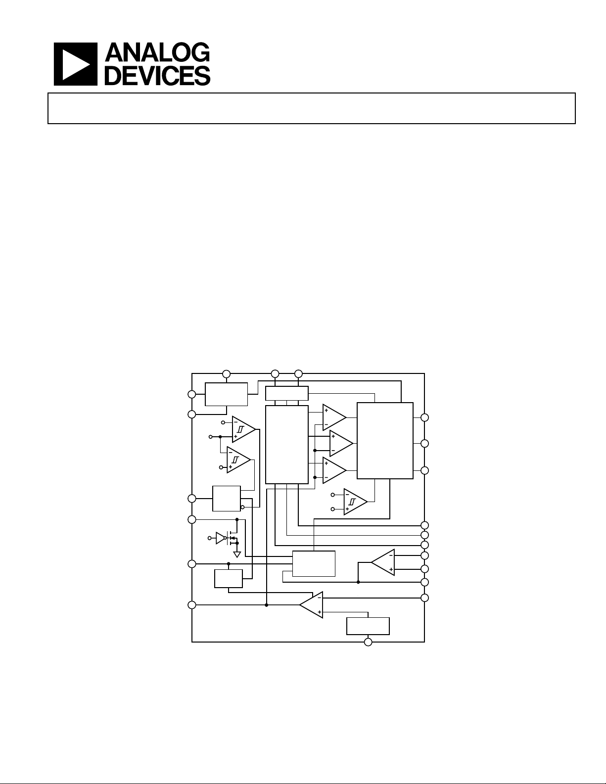
FUNCTIONAL BLOCK DIAGRAM
RAMPADJ
9
OSCILLATOR
CURRENT
BALANCING
CIRCUIT
EN
GND
PWRGD
ILIMIT
DELAY
COMP
6
14
5
10
EN
7
4
SHUTDOWN
950mV
FB
650mV
VCC
1
UVLO
& BIAS
DELAY
SOFT
START
RT
8
CURRENT
LIMIT
CIRCUIT
Synchronous Buck Controller
ADP3182
GENERAL DESCRIPTION
The ADP3182 is a highly efficient multiphase, synchronous,
buck-switching regulator controller optimized for converting a
12 V main supply into a high current, low voltage supply for use
in point-of-load (POL) applications. It uses a multimode PWM
architecture to drive the logic-level outputs at a programmable
switching frequency that can be optimized for VR size and
efficiency. The phase relationship of the output signals can be
programmed to provide 1-, 2-, or 3-phase operation, allowing
for the construction of up to three complementary buckswitching stages. The ADP3182 also provides accurate and
reliable short-circuit protection and adjustable current limiting.
ADP3182 is specified over the commercial temperature range of
0°C to +85°C and is available in a 20-lead QSOP package.
ENSET
20
19
18
17
16
15
12
11
13
3
PWM1
PWM2
PWM3
SW1
SW2
SW3
CSSUM
CSREF
CSCOMP
FB
CMP
CMP
1.05V
FB
RESET
RESET
CMP
RESET
CROWBAR CURRENT
2 / 3-PHASE
DRIVER LOGIC
LIMIT
ADP3182
Rev. 0
Information furnished by Analog Devices is believed to be accurate and reliable.
However, no responsibility is assumed by Analog Devices for its use, nor for any
infringements of patents or other rights of third parties that may result from its use.
Specifications subject to change without notice. No license is granted by implication
or otherwise under any patent or patent rights of Analog Devices. Trademarks and
registered trademarks are the property of their respective owners.
Figure 1.
800mV
REFERENCE
2
FBRTN
04938-001
One Technology Way, P.O. Box 9106, Norwood, MA 02062-9106, U.S.A.
Tel: 781.329.4700
www.analog.com
Fax: 781.326.8703 © 2004 Analog Devices, Inc. All rights reserved.

ADP3182
TABLE OF CONTENTS
Specifications..................................................................................... 3
Output Enable and UVLO ........................................................ 12
Test C ir c uit s ....................................................................................... 5
Absolute Maximum Ratings............................................................ 6
ESD Caution.................................................................................. 6
Pin Configuration and Function Description .............................. 7
Typical Performance Characteristics ............................................. 8
Theory of Operation ........................................................................ 9
Start-Up Sequence ........................................................................ 9
Master Clock Frequency .............................................................. 9
Output Voltage Differential Sensing .......................................... 9
Output Current Sensing .............................................................. 9
Current Control Mode and Thermal Balance ........................ 10
Volt a ge C o ntro l Mod e ................................................................10
Soft Start ......................................................................................10
Current Limit, Short-Circuit, and Latch-off Protection ....... 10
Power Good Monitoring ........................................................... 11
Applications..................................................................................... 14
Setting the Clock Frequency..................................................... 14
Soft Start and Current Limit Latch-Off Delay Time ............. 14
Inductor Selection...................................................................... 14
Output Current Sense................................................................ 15
Output Voltage............................................................................ 16
Power MOSFETs......................................................................... 16
Ramp Resistor Selection............................................................ 17
Current Limit Setpoint .............................................................. 17
Feedback Loop Compensation Design.................................... 17
Input Capacitor Selection and Input Current di/dt............... 18
Inductor DCR Temperature Correction ................................. 18
Layout and Component Placement ......................................... 19
Outline Dimensions ....................................................................... 20
Ordering Guide .......................................................................... 20
Output Crowbar .........................................................................11
REVISION HISTORY
10/04—Revision 0: Initial Version
Rev. 0 | Page 2 of 20

ADP3182
SPECIFICATIONS
VCC = 12 V, FBRTN = GND, TA = 0°C to 85°C, unless otherwise noted.
Table 1.
Parameter Symbol Conditions Min Typ Max Unit
OSCILLATOR
Frequency Range
Frequency Variation f
Output Voltage V
RAMPADJ Output Voltage V
RAMPADJ Input Current Range I
2
f
OSC
PHASE
RT
RAMPADJ
RAMPADJ
0.25 3 MHz
TA = 25°C, RT = 348 kΩ, 3-phase
= 25°C, RT = 174 kΩ, 3-phase
T
A
= 25°C, RT = 100 kΩ, 3-phase
T
A
RT = 100 kΩ to GND
RAMPADJ − FB −50 +50 mV
0 100
VOLTAGE ERROR AMPLIFIER
Output Voltage Range2 V
Accuracy V
Line Regulation
Input Bias Current I
FBRTN Current I
Output Current I
Gain Bandwidth Product GBW
COMP
FB
∆V
FB
FBRTN
O(ERR)
FB
(ERR)
Slew Rate C
0.7 3.1 V
Referenced to FBRTN 784 800 816 mV
VCC = 10 V to 14 V 0.05 %
FB = 800 mV −4 +4
100 140
FB forced to V
COMP = FB 20 MHz
= 10 pF 25
COMP
CURRENT SENSE AMPLIFIER
Offset Voltage V
Input Bias Current I
Gain Bandwidth Product GBW
OS(CSA)
BIAS(CSSUM)
(CSA)
Slew Rate C
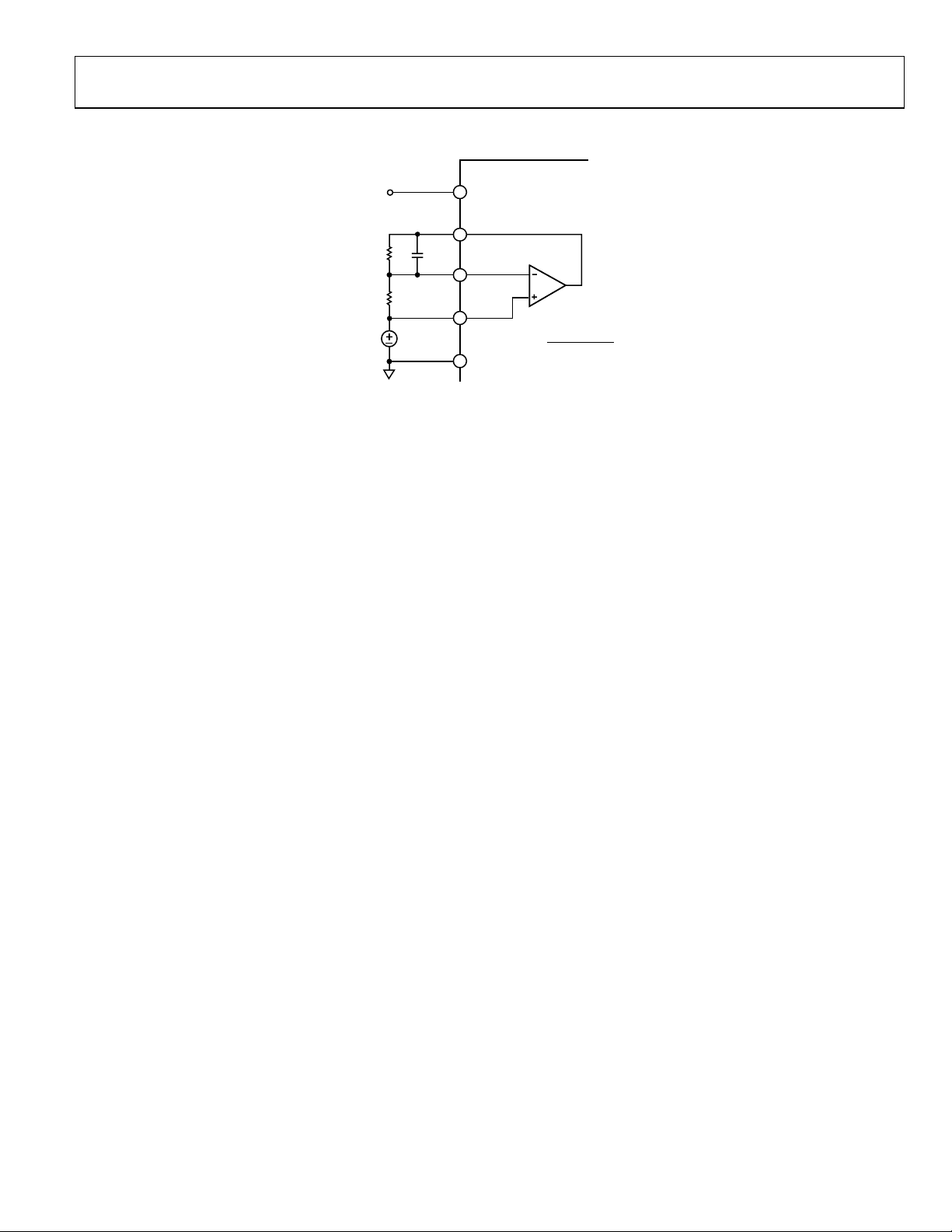
CSSUM − CSREF, Figure 2 −5.5 +5.5 mV
−50 +50 nA
10 MHz
= 10 pF 10
CSCOMP
Input Common-Mode Range CSSUM and CSREF 0 VCC − 2.5 V
Output Voltage Range 0.05 VCC − 2.5 V
Output Current I
CSCOMP
500
CURRENT BALANCE CIRCUIT
Common-Mode Range V
Input Resistance R
Input Current I
Input Current Matching
SW(X)CM
SW(X)
SW(X)
∆I
SW(X)
−600 +200 mV
SW(X) = 0 V 20 30 40
SW(X) = 0 V 4 7 10
SW(X) = 0 V −7 +7 %
CURRENT LIMIT COMPARATOR
Output Voltage
Normal Mode V
In Shutdown Mode V
Output Current, Normal Mode I
ILIMIT(NM)
ILIMIT(SD)
ILIMIT(NM)
EN > 2 V, R
EN < 0.8 V, I
EN > 2 V, R
Maximum Output Current2 60
Current Limit Threshold Voltage V
Current Limit Setting Ratio VCL/I
DELAY Normal Mode Voltage V
DELAY Overcurrent Threshold V
Latch-Off Delay Time t
CL
DELAY(NM)
DELAY(OC)
DELAY
V
R
R
R
CSREF
ILIMIT
DELAY
DELAY
DELAY
− V
CSCOMP
= 250 kΩ
= 250 kΩ
= 250 kΩ, C
SOFT START
Output Current, Soft Start Mode I
Soft Start Delay Time t
DELAY(SS)
DELAY(SS)
During start-up, DELAY < 2.4 V 15 20 25
R
= 250 kΩ, C
DELAY
1
155 200 245 kHz
400 kHz
600 kHz
1.9 2.0 2.1 V
− 3% 500
OUT
= 250 kΩ
ILIMIT
ILIMIT
= 250 kΩ
ILIMIT
, R
= −100 µA
= 250 kΩ
ILIMIT
2.9 3 3.1 V
400 mV
12
105 125 145 mV
10.4
2.9 3 3.1 V
1.7 1.8 1.9 V
DELAY
DELAY
= 12 nF
= 12 nF
1.5 ms
500
µA
µA
µA
µA
V/µs
V/µs
µA
kΩ
µA
µA
µA
mV/µA
µA
µs
Rev. 0 | Page 3 of 20

ADP3182
Parameter Symbol Conditions Min Typ Max Unit
ENABLE INPUT
Input Low Voltage V
Input High Voltage V
Input Current I
IL(EN)
IH(EN)
IN(EN)
POWER GOOD COMPARATOR
Undervoltage Threshold V
Overvoltage Threshold V
Output Low Voltage V
PWRGD(UV)
PWRGD(OV)
OL(PWRGD)IPWRGD(SINK)
Power Good Delay Time 200 ns
Crowbar Trip Point V
CROWBAR
Crowbar Reset Point Relative to FBRTN 550 650 750 mV
Crowbar Delay Time t
CROWBAR
PWM OUTPUTS
Output Low Voltage V
Output High Voltage V
OL(PWM)
OH(PWM)
SUPPLY
DC Supply Current 5 10 mA
UVLO Threshold Voltage V
UVLO
UVLO Hysteresis 0.7 0.9 1.1 V
1
All limits at temperature extremes are guaranteed via correlation using standard statistical quality control (SQC).
2
Guaranteed by design or bench characterization, not tested in production.
0.8 V
2.0 V
−1 +1
µA
Relative to FBRTN 600 660 720 mV
Relative to FBRTN 880 940 1000 mV
= 4 mA 225 400 mV
Relative to FBRTN 0.975 1.05 1.1 V
Overvoltage to PWM going low 400 ns
I
PWM(SINK)
I
PWM(SOURCE)
= −400 µA
= 400 µA
160 500 mV
4.0 5 V
VCC rising 6.5 6.9 7.3 V
Rev. 0 | Page 4 of 20

ADP3182
TEST CIRCUITS
ADP3182
1
100nF
V
CSCOMP
13
CSSUM
12
CSREF
11
14
GND
CC
CSCOMP –0.8V
VOS =
40
04938-002
OS
12V
39kΩ
1kΩ
0.8V
Figure 2. Current Sense Amplifier V
Rev. 0 | Page 5 of 20

ADP3182
ABSOLUTE MAXIMUM RATINGS
Table 2.
Parameter Rating
VCC −0.3 V to +15 V
FBRTN −0.3 V to +0.3 V
EN, DELAY, ILIMIT, RT,
PWM1 to PWM3, COMP
SW1 to SW3 −5 V to +25 V
All Other Inputs and Outputs −0.3 V to VCC + 0.3 V
Storage Temperature −65°C to +150°C
Operating Ambient Temperature Range 0°C to 85°C
Operating Junction Temperature 125°C
Thermal Impedance (θJA)
Lead Temperature
Soldering (10 s) 300°C
Infrared (15 s) 260°C
−0.3 V to 5.5 V
100°C/W
ESD CAUTION
ESD (electrostatic discharge) sensitive device. Electrostatic charges as high as 4000 V readily accumulate on
the human body and test equipment and can discharge without detection. Although this product features
proprietary ESD protection circuitry, permanent damage may occur on devices subjected to high energy
electrostatic discharges. Therefore, proper ESD precautions are recommended to avoid performance
degradation or loss of functionality.
Stresses above those listed under Absolute Maximum Ratings
may cause permanent damage to the device. This is a stress
rating only and functional operation of the device at these or
any other conditions above those indicated in the operational
section of this specification is not implied. Exposure to absolute
maximum rating conditions for extended periods may affect
device reliability. Absolute maximum ratings apply individually
only, not in combination. Unless otherwise specified, all other
voltages are referenced to GND.
Rev. 0 | Page 6 of 20
 Loading...