Analog Devices ADP3181 Datasheet

5-Bit or 6-Bit Programmable 2-,3-,4-Phase
V
FEATURES
Selectable 2-, 3- or 4-phase operation at up to 1 MHz per
phase
±14.5 mV worst-case mV differential sensing error over
temperature
Logic-level PWM outputs for interface to external high
power drivers
Active current balancing between all output phases
Built-in power good/crowbar blanking supports on-the-fly
VID code changes
Digitally programmable output can be switched between
VRM 9 (5-bit) and VRD 10 (6-bit) VID codes
Programmable short-circuit protection with programmable
latch-off delay
APPLICATIONS
Desktop PC power supplies for:
Next-generation Intel
VRM modules
GENERAL DESCRIPTION
The ADP3181 is a highly efficient multiphase synchronous
buck-switching regulator controller optimized for converting
a 12 V main supply into the core supply voltage required by
high performance Intel processors. It uses an internal 6-bit
DAC to read a voltage identification (VID) code directly from
the processor, which is used to set the output voltage. The
CPUID input selects whether the DAC codes match the
VRM 9 or VRD 10 specifications. It uses a multimode PWM
architecture to drive the logic-level outputs at a programmable
switching frequency that can be optimized for VR size and
efficiency. The phase relationship of the output signals can
be programmed to provide 2-, 3-, or 4-phase operation,
allowing for the construction of up to four complementary
buck-switching stages.
® processors
Synchronous Buck Controller
ADP3181
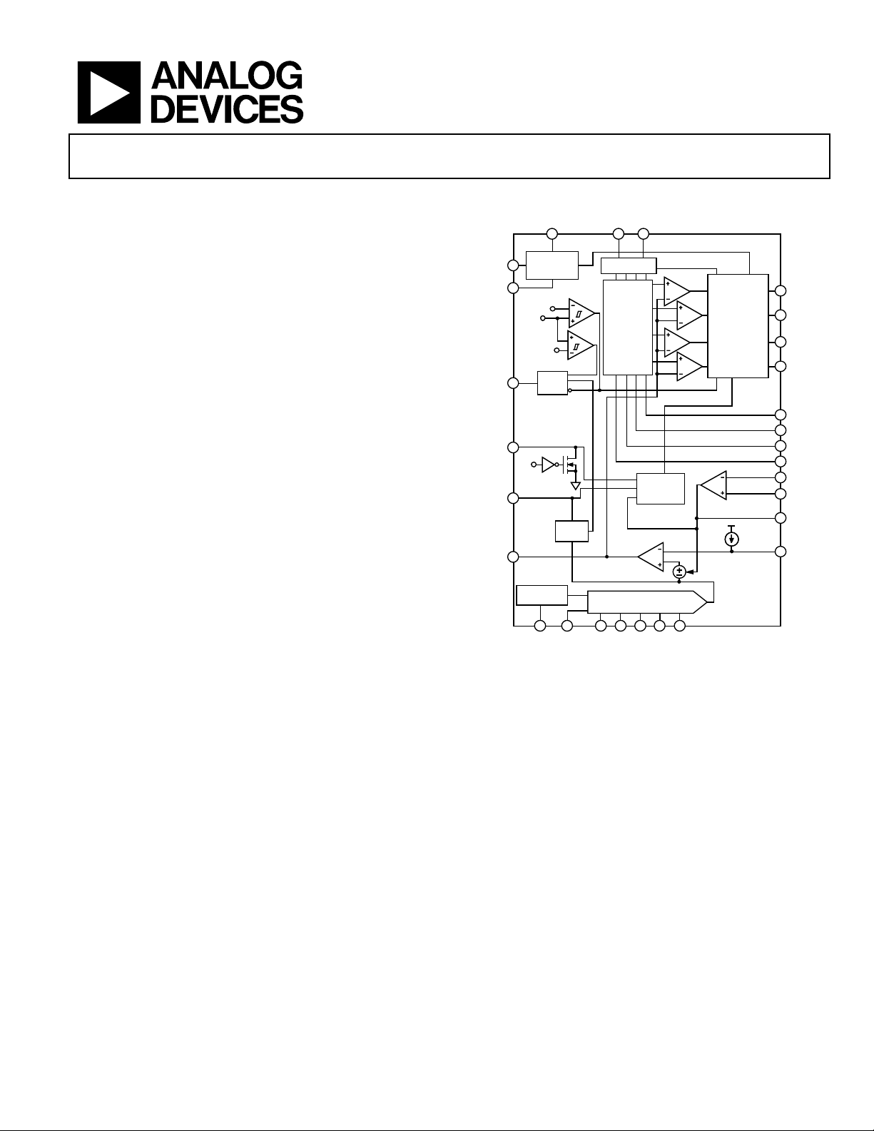
FUNCTIONAL BLOCK DIAGRAM
GND
PWRGD
ILIMIT
DELAY
COMP
11
EN
19
10
15
12
UVLO
SHUTDOWN
AND BIAS
DAC + 300mV
CSREF
DAC – 250mV
DELAY
EN
9
PRECISION
REFERENCE
CC
28 1314
SOFT
START
VID4 VID3 VID2 VID1 VID0FBRTN CPUID
OSCILLATOR
CURRENT-
BALANCING
CIRCUIT
VID
DAC
1234576
Figure 1.
RTRAMPADJ
CMP
CMP
CURRENT-
LIMITING
CIRCUIT
CMP
CMP
CROWBAR
ADP3181
ENSET
RESET
RESET
2-/3-/4-PHASE
DRIVER LOGIC
RESET
RESET
CURRENT
LIMIT
27
26
25
24
23
22
21
20
17
16
18
8
PWM1
PWM2
PWM3
PWM4
SW1
SW2
SW3
SW4
CSSUM
CSREF
CSCOMP
FB
04796-0-001
The ADP3181 also includes programmable no-load offset and
slope functions to adjust the output voltage as a function of the
load current so that it is always optimally positioned for a
system transient. The ADP3181 provides accurate and reliable
short-circuit protection, adjustable current limiting, and a
delayed power good output that accommodates on-the-fly
output voltage changes requested by the CPU.
The device is specified over the commercial temperature range
of 0°C to +85°C and is available in a 28-lead TSSOP package.
Rev. 0
Information furnished by Analog Devices is believed to be accurate and reliable.
However, no responsibility is assumed by Analog Devices for its use, nor for any
infringements of patents or other rights of third parties that may result from its use.
Specifications subject to change without notice. No license is granted by implication
or otherwise under any patent or patent rights of Analog Devices. Trademarks and
registered trademarks are the property of their respective owners.
One Technology Way, P.O. Box 9106, Norwood, MA 02062-9106, U.S.A.
Tel: 781.329.4700
Fax: 781.326.8703 © 2004 Analog Devices, Inc. All rights reserved.
www.analog.com

ADP3181
TABLE OF CONTENTS
Specifications..................................................................................... 3
Tes t Ci rc ui t s ....................................................................................... 5
Absolute Maximum Ratings............................................................ 6
Pin Configuration and Function Descriptions............................. 7
Typical Performance Characteristics............................................. 8
Theory of Operation ........................................................................ 9
Start-up Sequence......................................................................... 9
Master Clock Frequency............................................................ 10
Output Voltage Differential Sensing ........................................10
Output Current Sensing ............................................................ 11
Active Impedance Control Mode............................................. 11
Current Control Mode and Thermal Balance .......................11
Volt a ge C ont r o l Mo d e................................................................ 11
Soft Start ......................................................................................12
Current Limit, Short-Circuit, and Latch-Off Protection....... 12
Application Information................................................................ 15
Setting the Clock Frequency..................................................... 15
Soft-Start and Current-Limit Latch-Off Delay Times........... 15
Inductor Selection...................................................................... 15
Designing an Inductor............................................................... 16
Output Droop Resistance.......................................................... 16
Inductor DCR Temperature Correction ................................. 17
Output Offset.............................................................................. 17
C
Selection ............................................................................... 17
out
Power MOSFETS ........................................................................ 18
Ramp Resistor Selection............................................................ 19
Current Limit Setpoint.............................................................. 20
Feedback Loop Compensation Design.................................... 20
C
Selection and Input Current di/dt Reduction.................. 21
IN
Building a Switchable VR9/VR10 Design ............................... 22
Dynamic VID.............................................................................. 13
Power Good Monitoring ...........................................................13
Output Crowbar .........................................................................13
Output Enable and UVLO ........................................................ 13
REVISION HISTORY
5/04—Revision 0: Initial Version
Layout and Component Placement ............................................. 23
General Recommendations....................................................... 23
Outline Dimensions....................................................................... 24
Ordering Guide .......................................................................... 24
Rev. 0 | Page 2 of 24

ADP3181
SPECIFICATIONS
VCC = 12 V, FBRTN = GND, TA = 0°C to +85°C, unless otherwise noted.
Table 1.
Parameter Symbol Conditions Min Typ Max Unit
ERROR AMPLIFIER
Output Voltage Range
Accuracy V
2
V
COMP
FB
0.7 3.1 V
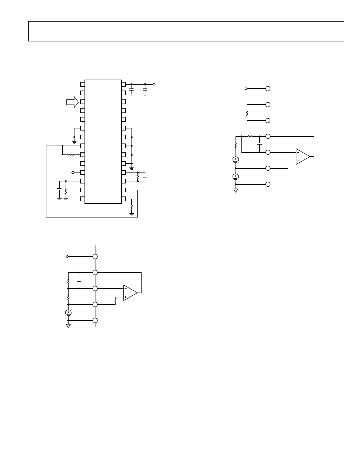
Relative to nominal DAC output, referenced to
FBRTN, CSSUM = CSCOMP. See Figure 2.
Line Regulation
Input Bias Current I
FBRTN Current I
Output Current I
∆V
FB
FBRTN
O(ERR)
FB
Gain Bandwidth Product GBW
Slew Rate C
VCC = 10 V to 14 V 0.05 %
14 15.5 17
100 140
FB forced to V
COMP = FB 20 MHz
(ERR)
= 10 pF 25
COMP
VID INPUTS
Input Low Voltage V
IL(VID)
CPUID > 4.5 V 0.8 V
CPUID < 4.0 V 0.4 V
Input High Voltage V
IH(VID)
CPUID > 4.5 V 2.0 V
CPUID < 4.0 V 0.8 V
Input Current I
VID
VID(x) = 0 V, CPUID > 4.5 V 40 70
VID(x) = 0 V, CPUID < 4.0 V 20 35
Pull-up Resistance R
VID
40 60
Internal Pull-up Voltage CPUID > 4.5 V 2.25 2.5 2.75 V
CPUID < 4.0 V 1.1 1.25 1.4 V
VID Transition Delay Time
2
VID code change to FB change 400 ns
No CPU Detection Turn-off Delay Time2 VID code change to 11111 to PWM going low 400 ns
CPUID INPUT
Input Low Voltage V
Input High Voltage V
IL(CPUID)
IH(CPUID)
0.4 V
0.8 4.0 V
VR 9 Detection Threshold Voltage 4.0 4.5 V
Input Current I
Pull-up Resistance R
CPUID
CPUID
CPUID = 0 V 20 3.5
4.0 60
OSCILLATOR
Frequency Range
Frequency Variation f
Output Voltage V
RAMPADJ Output Voltage V
RAMPADJ Input Current Range I
2
f
OSC
PHASE
RT
RAMPADJ
RAMPADJ
0.25 4 MHz
TA = 25°C, RT = 250 kΩ, 4-phase
= 25°C, RT = 115 kΩ, 4-phase
T
A
= 25°C, RT = 75 kΩ, 4-phase
T
A
RT = 100 kΩ to GND
RAMPADJ – FB
0 100
CURRENT SENSE AMPLIFIER
Offset Voltage V
Input Bias Current I
OS(CSA)
BIAS(CSSUM)
Gain Bandwidth Product GBW
Slew Rate C
CSSUM – CSREF. See Figure 3.
10 MHz
(CSA)
= 10 pF 10
CSCOMP
Input Common-Mode Range CSSUM and CSREF 0 2.7 V
Positioning Accuracy
∆V
FB
See Figure 4.
Output Voltage Range 0.05 2.7 V
Output Current I
CSCOMP
500
1
−14.5
– 3% 500
OUT
+14.5 mV
155 200 245 kHz
400 kHz
600 kHz
1.9 2.0 2.1 V
−50
−3
−50
+50 mV
+3 mV
+50 nA
−77 −80 −83
µA
µA
µA
V/µs
µA
µA
kΩ
µA
kΩ
µA
V/µs
mV
µA
Rev. 0 | Page 3 of 24

ADP3181
Parameter Symbol Conditions Min Typ Max Unit
CURRENT BALANCE CIRCUIT
Common-Mode Range V
Input Resistance R
Input Current I
Input Current Matching
SW(X)CM
SW(X)
SW(X)
∆I
SW(X)
CURRENT LIMIT COMPARATOR
Output Voltage
Normal Mode V
In Shutdown V
Output Current, Normal Mode I
Maximum Output Current
2
Current Limit Threshold Voltage V
ILIMIT(NM)
ILIMIT(SD)
ILIMIT(NM)
60
CL
Current Limit Setting Ratio VCL/I
DELAY Normal Mode Voltage V
DELAY Overcurrent Threshold V
Latch-off Delay Time t
DELAY(NM)
DELAY(OC)
DELAY
SOFT START
Output Current, Soft-start Mode I
Soft-start Delay Time t
DELAY(SS)
DELAY(SS)
ENABLE INPUT
Input Low Voltage V
Input High Voltage V
Input Current, Input Voltage Low I
Input Current, Input Voltage High I
IL(EN)
IH(EN)
IL(EN)
IH(EN)
POWER GOOD COMPARATOR
Undervoltage Threshold V
Overvoltage Threshold V
Output Low Voltage V
PWRGD(UV)
PWRGD(OV)
OL(PWRGD)IPWRGD(SINK)
Power Good Delay Time
During Soft Start2
VID Code Changing 100 250
VID Code Static 200 ns
Crowbar Trip Point V
CROWBAR
Crowbar Reset Point Relative to FBRTN 630 700 770 mV
Crowbar Delay Time t
CROWBAR
VID Code Changing 100 250
VID Code Static 400 ns
PWM OUTPUTS
Output Low Voltage V
Output High Voltage V
OL(PWM)
OH(PWM)
SUPPLY
DC Supply Current 5 10 mA
UVLO Threshold Voltage V
UVLO
UVLO Hysteresis 0.7 0.9 1.1 V
−600
SW(X) = 0 V 20 30 40
SW(X) = 0 V 4 7 10
SW(X) = 0 V
−5
+200 mV
kΩ
µA
+5 %
EN > 0.8 V, R
EN < 0.4 V, I
EN > 0.8 V, R
= 250 kΩ
ILIMIT
= −100 µA
ILIMIT
= 250 kΩ
ILIMIT
2.9 3 3.1 V
400 mV
12
µA
µA
V
R
R
R
CSREF
ILIMIT
DELAY
DELAY
DELAY
– V
= 250 kΩ
= 250 kΩ
= 250 kΩ, C
CSCOMP
, R
= 250 kΩ
ILIMIT
DELAY
= 12 nF
During start-up, DELAY < 2.4 V 15 20 25
R
= 250 kΩ, C
DELAY
= 12 nF, VID code = 011111
DELAY
105 125 145 mV
10.4
mV/µA
2.9 3 3.1 V
1.7 1.8 1.9 V
1.5 ms
µA
1 ms
0.4 V
0.8 V
EN = 0 V
−1
EN = 1.25 V 10 25
Relative to nominal DAC output
−180 −250 −320
1
µA
µA
mV
Relative to nominal DAC output 230 300 370 mV
= 4 mA 225 400 mV
R
DELAY
= 250 kΩ, C
= 12 nF, VID Code = 011111
DELAY
1 ms
µs
Relative to nominal DAC output 230 300 370 mV
Overvoltage to PWM going low
µs
I
PWM(SINK)
I
PWM(SOURCE)
= −400 µA
= 400 µA
160 500 mV
4.0 5 V
VCC rising 6.5 6.9 7.3 V
1
All limits at temperature extremes are guaranteed via correlation using standard statistical quality control (SQC).
2
Guaranteed by design or bench characterization, not tested in production.
Rev. 0 | Page 4 of 24

ADP3181
5
TEST CIRCUITS
ADP3181
VCC
PWM1
PWM2
PWM3
PWM4
SW1
SW2
SW3
SW4
GND
CSCOMP
CSSUM
CSREF
ILIMIT
-BIT CODE
12nF
1.25V
1kΩ
250kΩ
1
VID4
2
VID3
3
VID2
4
VID1
5
VID0
6
CPUID
7
FBRTN
8
FB
9
COMP
10
PWRGD
11
EN
12
DELAY
13
RT
14
RAMPADJ
Figure 2. Closed-Loop Output Voltage Accuracy
ADP3181
VCC
100nF
28
18
17
16
19
CSCOMP
CSSUM
CSREF
GND
VOS=
12V
39kΩ
1kΩ
1.0V
28
+
27
26
25
24
23
22
21
20
19
18
20kΩ
17
16
15
250kΩ
CSCOMP–1V
40
100nF1µF
100nF
04796-0-005
12V
04796-0-004
ADP3181
VCC
V = 80mV
∆
28
FB
8
COMP
9
CSCOMP
18
CSSUM
17
CSREF
16
GND
19
– FB
V = 0mV
∆
04796-0-006
200kΩ
∆
V
1.0V
12V
10kΩ
200kΩ
100nF
∆
VFB = FB
Figure 4. Positioning Voltage
Figure 3. Current Sense Amplifier V
OS
Rev. 0 | Page 5 of 24

ADP3181
ABSOLUTE MAXIMUM RATINGS
Table 2.
Parameter Rating
VCC
FBRTN
VID0 to VID4, CPUID, EN, DELAY, ILIMIT,
CSCOMP, RT, PWM1 to PWM4, COMP
SW1 to SW4
All other inputs and outputs
Storage temperature
Operating ambient temperature range 0°C to 85°C
Operating junction temperature 125°C
Thermal impedance (θJA) 100°C/W
Lead temperature
Soldering (10 sec) 300°C
Infrared (15 sec) 260°C
−0.3 V to +15 V
−0.3 V to +0.3 V
−0.3 V to +5.5 V
−5 V to +25 V
−0.3 V to VCC +0.3 V
−65°C to +150°C
ESD CAUTION
ESD (electrostatic discharge) sensitive device. Electrostatic charges as high as 4000 V readily accumulate on
the human body and test equipment and can discharge without detection. Although this product features
proprietary ESD protection circuitry, permanent damage may occur on devices subjected to high energy
electrostatic discharges. Therefore, proper ESD precautions are recommended to avoid performance
degradation or loss of functionality.
Stresses above those listed under Absolute Maximum Ratings
may cause permanent damage to the device. This is a stress
rating only; functional operation of the device at these or any
other conditions above those indicated in the operational
section of this specification is not implied. Exposure to absolute
maximum rating conditions for extended periods may affect
device reliability.
Absolute maximum ratings apply individually only, not in
combination. Unless otherwise specified all other voltages are
referenced to GND.
Rev. 0 | Page 6 of 24

ADP3181
PIN CONFIGURATION AND FUNCTION DESCRIPTIONS
VID4
VID3
VID2
VID1
VID0
CPUID
FBRTN
FB
COMP
PWRGD
EN
DELAY
RT
RAMPADJ
1
2
3
4
5
6
ADP3181
7
TOP VIEW
8
(Not to Scale)
9
10
11
12
13
14
28
27
26
25
24
23
22
21
20
19
18
17
16
15
VCC
PWM1
PWM2
PWM3
PWM4
SW1
SW2
SW3
SW4
GND
CSCOMP
CSSUM
CSREF
ILIMIT
04796-0-011
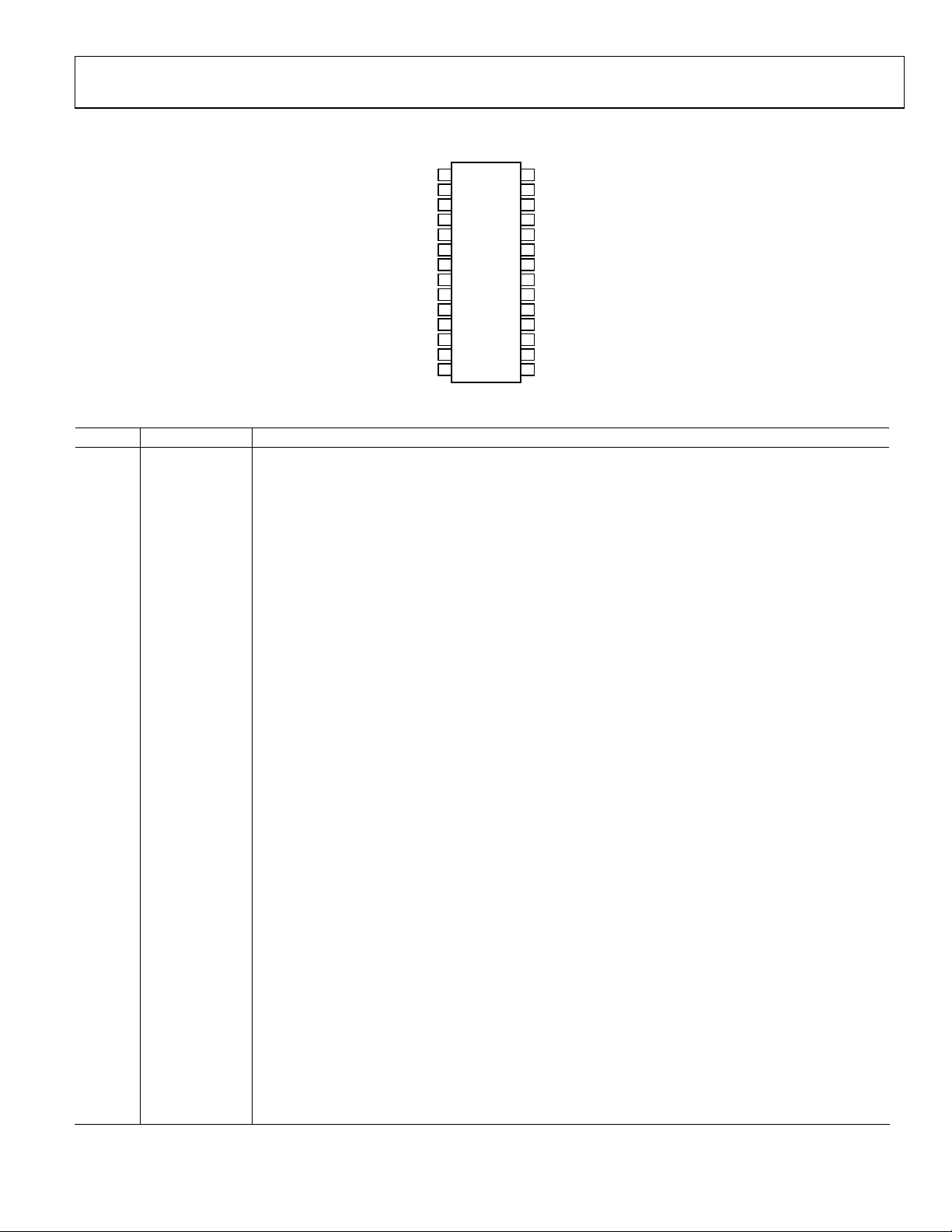
Figure 5. Pin Configuration
Table 3. Pin Function Descriptions
Pin No. Name Description
1 to 5 VID4 to VID0 Voltage Identification DAC Inputs. These five pins are pulled up to an internal reference, providing a
Logic 1 if left open. When in normal mode, the DAC output programs the FB regulation voltage based
on the condition of the CPUID pin (see Table 4 and Table 5). Leaving VID4 through VID0 open results in the
ADP3181 going into a “no CPU” mode, shutting off its PWM outputs.
6 CPUID
CPU DAC Code Selection Input. When this pin is pulled > 4.5 V, the internal DAC reads its inputs based on
the VR 9 VID table (see Table 4). When this pin is < 4 V, the DAC reads its inputs based on the VR 10 VID
table (see Table 5) and treats CPUID as the VID5 input.
7 FBRTN Feedback Return. VID DAC and error amplifier reference for remote sensing of the output voltage.
8 FB
Feedback Input. Error amplifier input for remote sensing of the output voltage. An external resistor
between this pin and the output voltage sets the no-load offset point.
9 COMP Error Amplifier Output and Compensation Point.
10 PWRGD
Power Good Output. Open-drain output that signals when the output voltage is outside of the proper
operating range.
11 EN Power Supply Enable Input. Pulling this pin to GND disables the PWM outputs.
12 DELAY
Soft-start Delay and Current Limit Latch-off Delay Setting Input. An external resistor and capacitor
connected between this pin and GND sets the soft-start ramp-up time and the overcurrent latch-off
delay time.
13 RT
Frequency Setting Resistor Input. An external resistor connected between this pin and GND sets the
oscillator frequency of the device.
14 RAMPADJ
PWM Ramp Current Input. An external resistor from the converter input voltage to this pin sets the internal
PWM ramp.
15 ILIMIT
Current Limit Setpoint/Enable Output. An external resistor from this pin to GND sets the current limit
threshold of the converter. This pin is actively pulled low when the ADP3181 EN input is low, or when VCC
is below its UVLO threshold, to signal to the driver IC that the driver high-side and low-side outputs should
go low.
16 CSREF
Current Sense Reference Voltage Input. The voltage on this pin is used as the reference for the current
sense amplifier and the power good and crowbar functions. This pin should be connected to the common
point of the output inductors.
17 CSSUM
Current Sense Summing Node. External resistors from each switch node to this pin sum the average
inductor currents together to measure the total output current.
18 CSCOMP
Current Sense Compensation Point. A resistor and capacitor from this pin to CSSUM determine the slope of
the load line and the positioning loop response time.
19 GND Ground. All internal biasing and the logic output signals of the device are referenced to this ground.
20 to 23 SW4 to SW1
Current Balance Inputs. Inputs for measuring the current level in each phase. The SW pins of unused
phases should be left open.
24 to 27 PWM4 to PMW1
Logic-level PWM Outputs. Each output is connected to the input of an external MOSFET driver such as the
ADP3413 or ADP3418. Connecting the PWM3 and/or PWM4 outputs to GND causes that phase to turn off,
allowing the ADP3181 to operate as a 2-, 3-, or 4-phase controller.
28 VCC Supply Voltage for the Device.
Rev. 0 | Page 7 of 24

ADP3181
TYPICAL PERFORMANCE CHARACTERISTICS
4
3
2
1
MASTER CLOCK FREQUENCY (MHz)
0
0 50 100 150 200 250 300
Figure 6. Master Clock Frequency vs. R
5.3
TA = 25°C
4-PHASE OPERATION
5.2
5.1
5.0
4.9
4.8
SUPPLY CURRENT (mA)
4.7
4.6
0 4.03.53.02.52.01.51.00.5
RT VALUE (kΩ)
T
OSCILLATOR FREQUENCY (MHz)
Figure 7. Supply Current vs. Oscillator Frequency
04796-0-002
04796-0-003
Rev. 0 | Page 8 of 24
 Loading...