4-Bit Programmable
a
FEATURES
Optimally Compensated Active Voltage Positioning
with Gain and Offset Adjustment (ADOPT™) for
Superior Load Transient Response
Complies with VRM 8.4 Specifications with Lowest
System Cost
4-Bit Digitally Programmable 1.3 V to 2.05 V Output
N-Channel Synchronous Buck Driver
Two On-Board Linear Regulator Controllers
Total Accuracy 0.8% Over Temperature
High Efficiency Current-Mode Operation
Short Circuit Protection
Power Good Output
Overvoltage Protection Crowbar Protects Micro-
processors with No Additional External Components
APPLICATIONS
Core Supply Voltage Generation for:
Intel Pentium
Intel Celeron™
®
III
Synchronous Buck Controllers
ADP3159/ADP3179
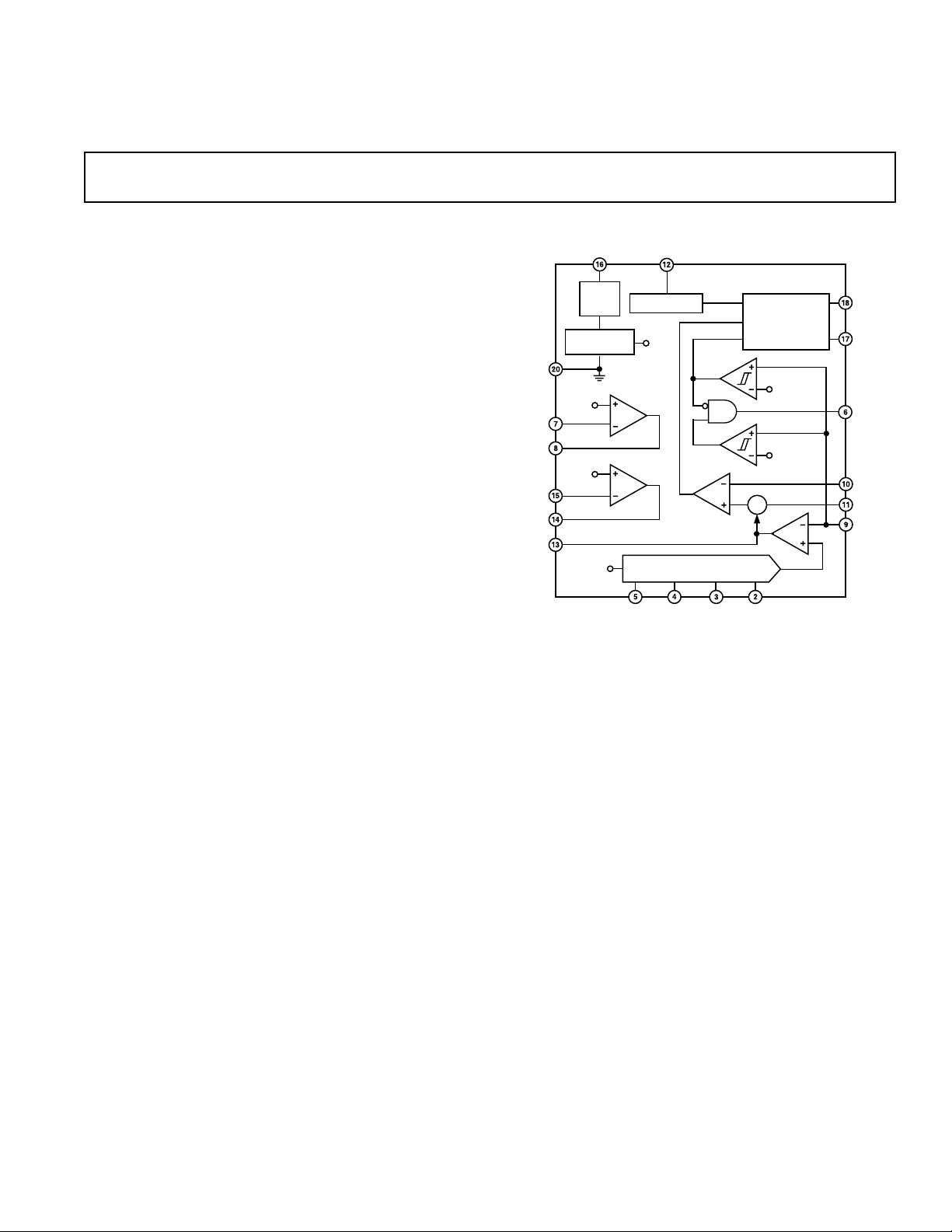
FUNCTIONAL BLOCK DIAGRAM
GND
LRFB1
LRDRV1
LRFB2
LRDRV2
COMP
VCC
UVLO
& BIAS
REFERENCE
V
LR1
V
LR2
REF
CT
OSCILLATOR
REF
VID DAC
ADP3159/ADP3179
SET
RESET
CROWBAR
CMP
DRIVE
+–
PWM
DAC+20%
DAC–20%
g
m
DRVH
DRVL
PWRGD
CS–
CS+
FB
GENERAL DESCRIPTION
The ADP3159 and ADP3179 are highly efficient output synchronous buck switching regulator controllers optimized for
converting a 5 V main supply into the core supply voltage
required by high-performance processors. These devices use an
internal 4-bit DAC to read a voltage identification (VID) code
directly from the processor, which is used to set the output
voltage between 1.3 V and 2.05 V. They use a current mode,
constant off-time architecture to drive two N-channel
MOSFETs at a programmable switching frequency that can be
optimized for regulator size and efficiency.
The ADP3159 and ADP3179 also use a unique supplemental
regulation technique called Analog Devices Optimal Positioning Technology (ADOPT) to enhance load transient
performance. Active voltage positioning results in a dc/dc converter that meets the stringent output voltage specifications
for high-performance processors, with the minimum number
ADOPT is a trademark of Analog Devices, Inc.
Pentium is a registered trademark of Intel Corporation.
Celeron is a trademark of Intel Corporation.
VID3 VID2 VID1 VID0
of output capacitors and smallest footprint. Unlike voltagemode and standard current-mode architectures, active voltage
positioning adjusts the output voltage as a function of the load
current so it is always optimally positioned for a system transient. The devices also provide accurate and reliable short
circuit protection and adjustable current limiting. They also
include an integrated overvoltage crowbar function to protect
the microprocessor from destruction in case the core supply
exceeds the nominal programmed voltage by more than 20%.
The ADP3159 and ADP3179 contain two fixed-output voltage linear regulator controllers that are designed to drive
external N-channel MOSFETs. The outputs are internally
fixed at 2.5 V and 1.8 V in the ADP3159, while the ADP3179
provides adjustable output, which is set using an external
resistor divider. These linear regulators are used to generate
the auxiliary voltages (AGP, GTL, etc.) required in most motherboard designs, and have been designed to provide a high
bandwidth load-transient response.
The ADP3159 and ADP3179 are specified over the commercial
temperature range of 0°C to 70°C and are available in a 20-lead
TSSOP package.
REV. A
Information furnished by Analog Devices is believed to be accurate and
reliable. However, no responsibility is assumed by Analog Devices for its
use, nor for any infringements of patents or other rights of third parties that
may result from its use. No license is granted by implication or otherwise
under any patent or patent rights of Analog Devices.
One Technology Way, P.O. Box 9106, Norwood, MA 02062-9106, U.S.A.
Tel: 781/329-4700 www.analog.com
Fax: 781/326-8703 © Analog Devices, Inc., 2001

1
ADP3159/ADP3179–SPECIFICATIONS
Parameter Symbol Conditions Min Typ Max Unit
FEEDBACK INPUT
Output Accuracy V
1.3 V Output Figure 1 1.289 1.3 1.311 V
1.65 V Output Figure 1 1.637 1.65 1.663 V
2.05 V Output Figure 1 2.034 2.05 2.066 V
Line Regulation ∆V
Crowbar Trip Point V
Crowbar Reset Point % of Nominal DAC Voltage 40 50 60 %
Crowbar Response Time t
VID INPUTS
Input Low Voltage V
Input High Voltage V
Input Current I
Pull-Up Resistance R
Internal Pull-Up Voltage 5.0 5.4 5.7 V
OSCILLATOR
Off Time T
CT Charge Current I
ERROR AMPLIFIER
Output Resistance R
Transconductance g
Output Current I
Maximum Output Voltage V
Output Disable Threshold V
–3 dB Bandwidth BW
CURRENT SENSE
Threshold Voltage V
Input Bias Current I
Response Time t
OUTPUT DRIVERS
Output Resistance R
Output Transition Time tR, t
LINEAR REGULATORS
Feedback Current I
LR1 Feedback Voltage
LR2 Feedback Voltage
Driver Output Voltage V
POWER GOOD COMPARATOR
Undervoltage Threshold V
Undervoltage Hysteresis % of Nominal DAC Voltage 5 %
Overvoltage Threshold V
Overvoltage Reset Point % of Nominal DAC Voltage 40 50 60 %
Output Voltage Low V
Response Time 250 ns
SUPPLY
DC Supply Current
2
UVLO Threshold Voltage V
UVLO Hysteresis 0.8 1 1.2 V
NOTES
1
All limits at temperature extremes are guaranteed via correlation using standard Statistical Quality Control (SQC).
2
Dynamic supply current is higher due to the gate charge being delivered to the external MOSFETs.
Specifications subject to change without notice.
FB
OUT
CROWBAR
CROWBAR
IL(VID)
IH(VID)
VID
VID
CT
VCC = 10 V to 14 V 0.06 %
% of Nominal DAC Voltage 115 120 125 %
Overvoltage to DRVL Going High 400 ns
VID(X) = 0 V 185 250 µA
= 25°C, CT = 200 pF 3.5 4.0 4.5 µs
A
TA = 25°C, V
TA = 25°C, V
O(ERR)
m(ERR)
O(ERR)
COMP(MAX)
COMP(OFF)
ERR
CS(TH)
FB– Forced to V
FB– Forced to V
COMP = Open 500 kHz
FB– Forced to V
FB– ≤ 0.45 V 35 45 54 mV
0.8 V ≤ COMP ≤ 1 V 1 5 mV
CS+
CS
, I
CS+ = CS– = V
CS–
CS+ – (CS–) > 87 mV to DRVH 50 ns
Going Low
O(DRV(X))IL
F
LRFB(X)
V
LRFB(1)
= 50 mA 6 Ω
CL = 3000 pF 80 ns
ADP3159 Figure 2, VCC = 4.5 V to 12.6 V 2.44 2.5 2.56 V
ADP3179 Figure 2, VCC = 2-4.5 V to 12.6 V 0.97 1.0 1.03 V
V
LRFB(2)
ADP3159 Figure 2, VCC = 4.5 V to 12.6 V 1.75 1.8 1.85 V
ADP3179 Figure 2, VCC = 2-4.5 V to 12.6 V 0.97 1.0 1.03 V
LRDRV(X)
PWRGD(UV)
PWRGD(OV)
OL(PWRGD)IPWRGD(SINK)
I
CC
UVLO
VCC = 4.5 V, V
% of Nominal DAC Voltage 75 80 85 %
% of Nominal DAC Voltage 115 120 125 %
in Regulation 130 150 170 µA
OUT
= 0 V 25 35 45 µA
OUT
OUT
OUT
OUT
OUT
LRFB(X)
= 1 mA 250 500 mV
(VCC = 12 V, TA = 0C to 70C, unless otherwise noted.)
0.6 V
2.0 V
20 30 kΩ
1mΩ
2.05 2.2 2.35 mmho
– 3% 625 µA
– 3% 3.0 V
600 750 900 mV
– 3% 69 78 87 mV
0.5 5 µA
0.3 1 µA
= 0 V 4.2 V
79mA
6.75 7 7.25 V
–2–
REV. A

ADP3159/ADP3179
WARNING!
ESD SENSITIVE DEVICE
ABSOLUTE MAXIMUM RATINGS*
VCC . . . . . . . . . . . . . . . . . . . . . . . . . . . . . . . –0.3 V to +15 V
DRVH, DRVL, LRDRV1, LRDRV2 . . . . –0.3 V to VCC + 0.3 V
All Other Inputs and Outputs . . . . . . . . . . . . –0.3 V to +10 V
Operating Ambient Temperature Range . . . . . . . 0°C to 70°C
Operating Junction Temperature . . . . . . . . . . . . . . . . . 125°C
Storage Temperature Range . . . . . . . . . . . . –65°C to +150°C
. . . . . . . . . . . . . . . . . . . . . . . . . . . . . . . . . . . . . . 143°C/W
θ
JA
Lead Temperature (Soldering, 10 sec) . . . . . . . . . . . . 300°C
Vapor Phase (60 sec) . . . . . . . . . . . . . . . . . . . . . . . . . . 215°C
Infrared (15 sec) . . . . . . . . . . . . . . . . . . . . . . . . . . . . . 220°C
*This is a stress rating only; operation beyond these limits can cause the device to
be permanently damaged. Unless otherwise specified, all voltages are referenced
to GND.
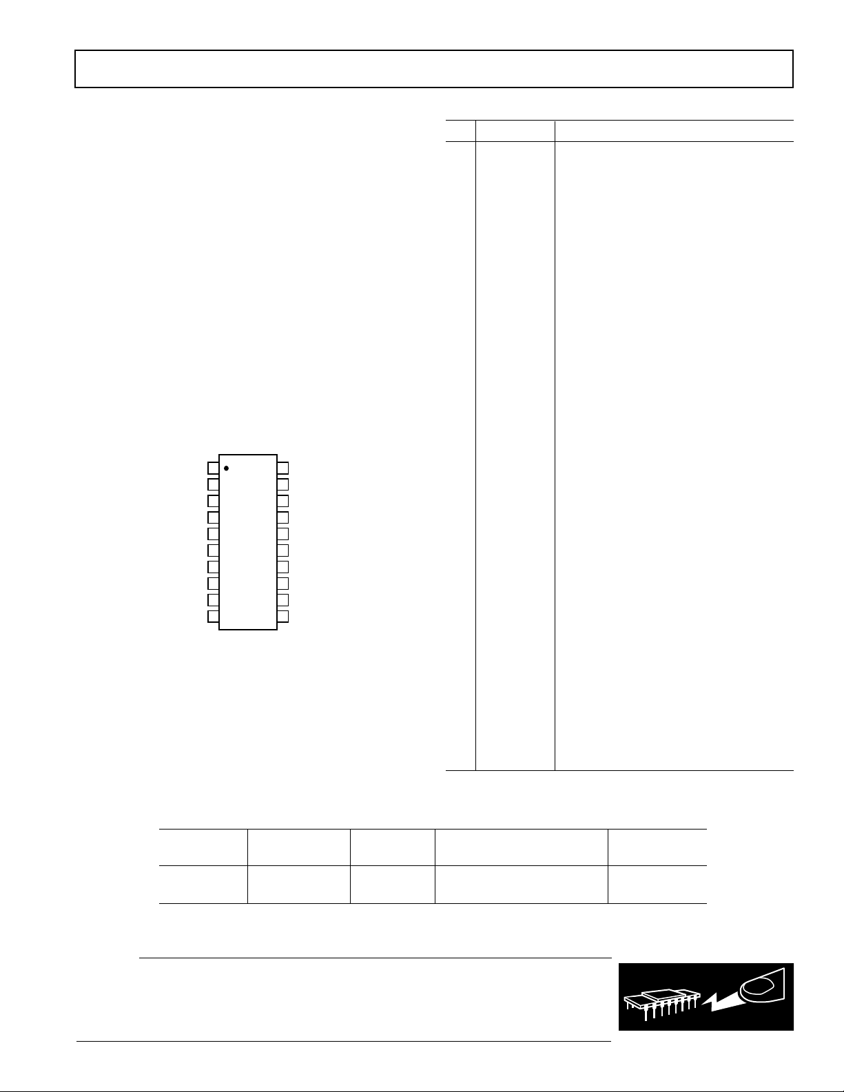
PIN CONFIGURATION
RU-20
NC
VID0
VID1
VID2
VID3
PWRGD
LRFB1
LRDRV1
FB
CS–
1
2
3
4
ADP3159/
5
ADP3179
6
TOP VIEW
(Not to Scale)
7
8
9
10
NC = NO CONNECT
20
19
18
17
16
15
14
13
12
11
GND
NC
DRVH
DRVL
VCC
LRFB2
LRDRV2
COMP
CT
CS+
PIN FUNCTION DESCRIPTIONS
Pin Mnemonic Function
1, 19 NC No Connection.
2–5 VID3, VID2, Voltage Identification DAC Inputs. These
VID1, VID0 pins are pulled up to an internal reference,
providing a Logic One if left open. The
DAC output programs the FB regulation
voltage from 1.3 V to 2.05 V.
6 PWRGD Open drain output that signals when the
output voltage is in the proper operating
range.
7, 15 LRFB1, Feedback connections for the linear
LRFB2 regulator controllers.
8, 14 LRDRV1, Gate drives for the respective linear
LRDRV2 regulator N-channel MOSFETs.
9 FB Feedback Input. Error amplifier input for
remote sensing of the output voltage.
10 CS– Current Sense Negative Node. Negative
input for the current comparator.
11 CS+ Current Sense Positive Node. Positive
input for the current comparator. The
output current is sensed as a voltage at this
pin with respect to CS–.
12 CT External capacitor connected from CT to
ground sets the Off-time of the device.
13 COMP Error Amplifier Output and Compensation
Point. The voltage at this output programs
the output current control level between
CS+ and CS–.
16 VCC Supply Voltage for the device.
17 DRVL Low-Side MOSFET Drive. Gate drive for
the synchronous rectifier N-channel
MOSFET. The voltage at DRVL swings
from GND to VCC.
18 DRVH High-side MOSFET Drive. Gate drive for
the buck switch N-channel MOSFET.
The voltage at DRVH swings from GND
to VCC.
20 GND Ground Reference. GND should have a
low impedance path to the source of hte
synchronous MOSFET.
ORDERING GUIDE
Temperature LDO Package Package
Model Range Voltage Description Option
ADP3159JRU 0°C to 70°C 2.5 V, 1.8 V Thin Shrink Small Outline RU-20
ADP3179JRU 0°C to 70°C Adjustable Thin Shrink Small Outline RU-20
CAUTION
ESD (electrostatic discharge) sensitive device. Electrostatic charges as high as 4000 V readily
accumulate on the human body and test equipment and can discharge without detection. Although
the ADP3159 and the ADP3179 feature proprietary ESD protection circuitry, permanent damage
may occur on devices subjected to high-energy electrostatic discharges. Therefore, proper ESD
precautions are recommended to avoid performance degradation or loss of functionality.
REV. A
–3–

ADP3159/ADP3179
–Typical Performance Characteristics
60
50
40
30
20
SUPPLY CURRENT – mA
10
0
0 100 200 300 400 500 600 700 800
OSCILLATOR FREQUENCY – kHz
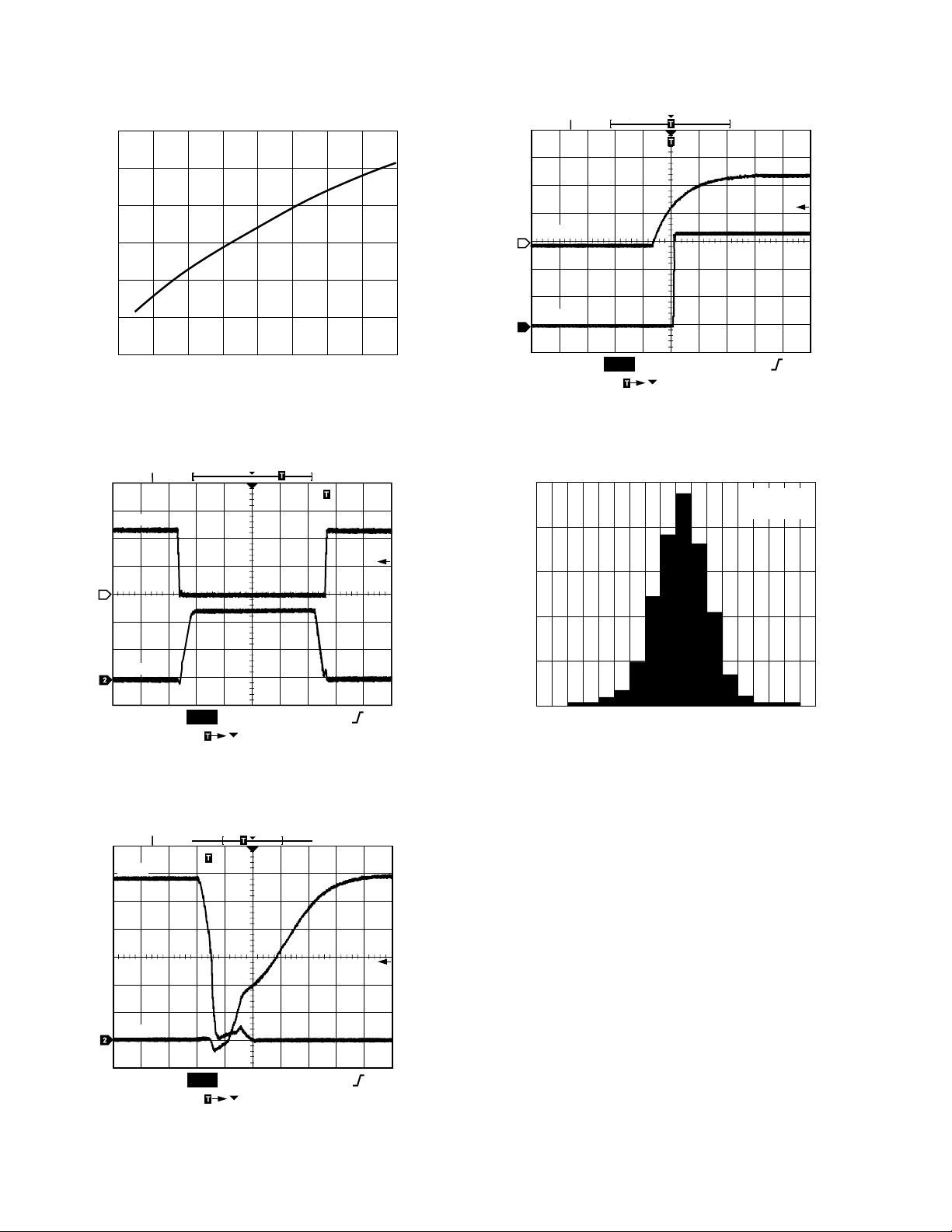
TPC 1. Supply Current vs. Operating Frequency Using
MOSFETs of Figure 3
TEK RUN TRIG'D
DRVH
TEK RUN TRIG'D
V
CC
1
V
CORE
2
CH1
5.00V CH2 500mV BW M 10.0ms A CH1
W
0.00000 s
TPC 4. Power-On Start-Up Waveform
25
20
TA = 25C
V
= 1.65V
OUT
5.90VB
1
DRVL
CH1
5.00V CH2 5.00V BW M 1.00s A CH1
W
–2.6500s
5.90VB
TPC 2. Gate Switching Waveforms Using MOSFETs of
Figure 3
TEK RUN TRIG'D
DRVH
15
10
NUMBER OF PARTS – %
5
0
–0.5
OUTPUT ACCURACY – % of Nominal
0 0.5
TPC 5. Output Accuracy Distribution
DRVL
CH1
2.00V CH2 2.00V BW M 1.00ns A
W
150.000s
CH1
5.88VB
TPC 3. Driver Transition Waveforms Using MOSFETs of
Figure 3
–4–
REV. A

ADP3159/ADP3179
ADP3159/
ADP3179
4-BIT CODE
V
FB
1
NC
2
VID0
3
VID1
4
VID2
5
VID3
6
PWRGD
7
LRFB1
8
LRDRV1
9
FB
10
CS–
NC = NO CONNECT
GND
NC
DRVH
DRVL
VCC
LRFB2
LRDRV2
COMP
CT
CS+
20
19
18
17
16
+
1F
15
14
13
12
11
1.2V
12V
100nF
100
100nF
AD820
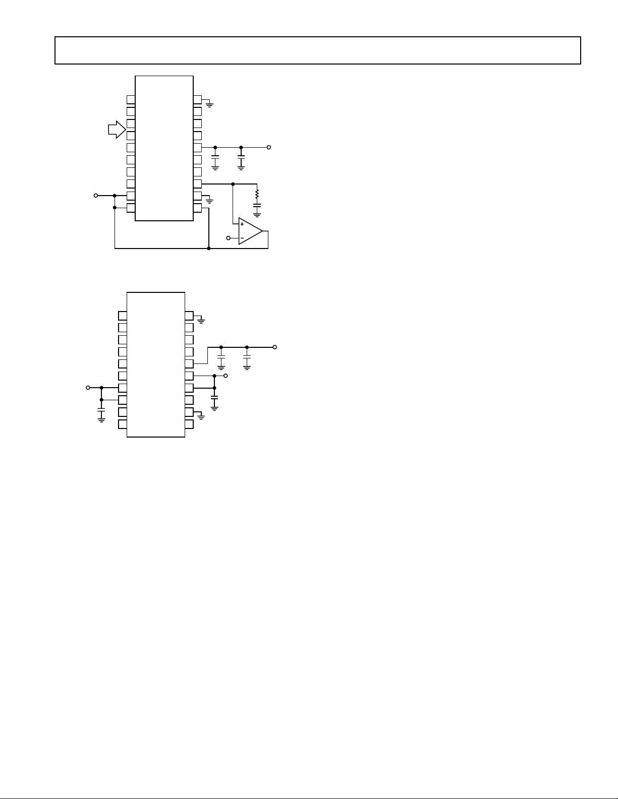
Figure 1. Closed Loop Output Voltage Accuracy
Test Circuit
ADP3159/
ADP3179
1
NC
2
VID0
3
VID1
4
VID2
5
VID3
6
PWRGD
V
LR1
10nF
7
LRFB1
8
LRDRV1
9
FB
10
CS–
NC = NO CONNECT
GND
NC
DRVH
DRVL
VCC
LRFB2
LRDRV2
COMP
CS+
CT
20
19
18
17
16
15
14
13
12
11
+
10nF
1F
V
LR2
VCC
100nF
Figure 2. Linear Regulator Output Voltage Accuracy
Test Circuit
THEORY OF OPERATION
The ADP3159 and ADP3179 use a current-mode, constant
off-time control technique to switch a pair of external N-channel
MOSFETs in a synchronous buck topology. Constant off-time
operation offers several performance advantages, including that no
slope compensation is required for stable operation. A unique
feature of the constant off-time control technique is that since
the off-time is fixed, the converter’s switching frequency is a
function of the ratio of input voltage to output voltage. The fixed
off-time is programmed by the value of an external capacitor
connected to the CT pin. The on-time varies in such a way
that a regulated output voltage is maintained as described below
in the cycle-by-cycle operation. The on-time does not vary under
fixed input supply conditions, and it varies only slightly as a function of load. This means that the switching frequency remains
fairly constant in a standard computer application.
Active Voltage Positioning
The output voltage is sensed at the CS– pin. A voltage error
amplifier, (g
), amplifies the difference between the output
m
voltage and a programmable reference voltage. The reference
voltage is programmed to between 1.3 V and 2.05 V by an internal 4-bit DAC that reads the code at the voltage identification
(VID) pins (Refer to Table I for output voltage vs. VID pin code
information). A unique supplemental regulation technique called
Analog Devices Optimal Positioning Technology (ADOPT)
adjusts the output voltage as a function of the load current so
that it is always optimally positioned for a load transient. Standard (passive) voltage positioning, sometimes recommended for
use with other architectures, has poor dynamic performance
which renders it ineffective under the stringent repetitive transient conditions specified in Intel VRM documents. Consequently,
such techniques do not allow the minimum possible number of
output capacitors to be used. ADOPT, as used in the ADP3159
and ADP3179, provides a bandwidth for transient response that
is limited only by parasitic output inductance. This yields optimal load transient response with the minimum number of
output capacitors.
Cycle-by-Cycle Operation
During normal operation (when the output voltage is regulated),
the voltage error amplifier and the current comparator are the
main control elements. During the on-time of the high-side
MOSFET, the current comparator monitors the voltage between
the CS+ and CS– pins. When the voltage level between the two
pins reaches the threshold level, the DRVH output is switched to
ground, which turns off the high-side MOSFET. The timing
capacitor CT is then charged at a rate determined by the off-time
controller. While the timing capacitor is charging, the DRVL
output goes high, turning on the low-side MOSFET. When the
voltage level on the timing capacitor has charged to the upper
threshold voltage level, a comparator resets a latch. The output
of the latch forces the low-side drive output to go low and the
high-side drive output to go high. As a result, the low-side switch
is turned off and the high-side switch is turned on. The sequence
is then repeated. As the load current increases, the output voltage starts to decrease. This causes an increase in the output of
the voltage-error amplifier, which, in turn, leads to an increase
in the current comparator threshold, thus tracking the load current. To
prevent cross conduction of the external MOSFETs, feedback is
incorporated to sense the state of the driver output pins. Before
the low-side drive output can go high, the high-side drive output
must be low. Likewise, the high-side drive output is unable to
go high while the low-side drive output is high.
Power Good
The ADP3159 has an internal monitor that senses the output
voltage and drives the PWRGD pin of the device. This pin is an
open drain output whose high level (when connected to a pull-up
resistor) indicates that the output voltage has been within a ±20%
regulation band of the targeted value for more than 500 ms. The
PWRGD pin will go low if the output is outside the regulation
band for more than 500 ms.
Output Crowbar
An added feature of using an N-channel MOSFET as the synchronous switch is the ability to crowbar the output with the same
MOSFET. If the output voltage is 20% greater than the targeted
value, the controller IC will turn on the lower MOSFET,
which will current-limit the source power supply or blow its fuse,
pull down the output voltage, and thus save the microprocessor
from destruction. The crowbar function releases at approximately
50% of the nominal output voltage. For example, if the output
is programmed to 1.5 V, but is pulled up to 1.85 V or above, the
crowbar will turn on the lower MOSFET. If in this case the output
is pulled down to less than 0.75 V, the crowbar will release,
allowing the output voltage to recover to 1.5 V if the fault
condition has been removed.
REV. A
–5–
 Loading...