Analog Devices ADP3171 a Datasheet

Synchronous Buck Controller
a
FEATURES
Fixed 1.2 V N-Channel Synchronous Buck Driver
Two On-Board Linear Regulator Controllers
Total Accuracy ±1% over Temperature
High Efficiency Current-Mode Operation
Short-Circuit Protection
Power Good Output
Overvoltage Protection Crowbar Protects Switching
Output with No Additional External Components
APPLICATIONS
Auxiliary System Supplies for Desktop
Computer Systems
General-Purpose Low Voltage Supplies
with Dual Linear Regulator Controllers
ADP3171
FUNCTIONAL BLOCK DIAGRAM
GND
LRFB1
LRDRV1
LRFB2
LRDRV2
COMP
REFERENCE
1
1.5V
3
4
1.8V
VCC
UVLO
AND BIAS
ADP3171
CT
8
OSCILLATOR
REF
SET
RESET
CROWBAR
CMP
PWM
LOGIC
DAC +20%
DAC –20%
g
m
1.2V
7
5
DRVH
DRVL
PWRGD
CS–
CS+
FB
GENERAL DESCRIPTION
The ADP3171 is a highly efficient output synchronous buck
switching regulator controller optimized for converting a 5 V
main supply into the auxiliary supply voltages required by
processors and chipsets. The ADP3171 provides a fixed
output voltage of 1.2 V at up to 15 A, depending on the
power ratings of the external MOSFETs and inductor. The
ADP3171 uses a current-mode, constant off time architecture to
drive two N-channel MOSFETs at a programmable switching
frequency that can be optimized for regulator size and efficiency.
The ADP3171 provides accurate and reliable short circuit
protection and adjustable current limiting. It also includes an
integrated overvoltage crowbar function to protect the load in
case the output voltage exceeds the nominal programmed
by more than 20%.
voltage
The ADP3171 contains two fixed output voltage linear regulator
controllers that are designed to drive external N-channel
MOSFETs. These linear regulators are used to generate the
auxiliary voltages required in most motherboard designs and have
been designed to provide a high bandwidth load transient response.
The ADP3171 is specified over the commercial temperature
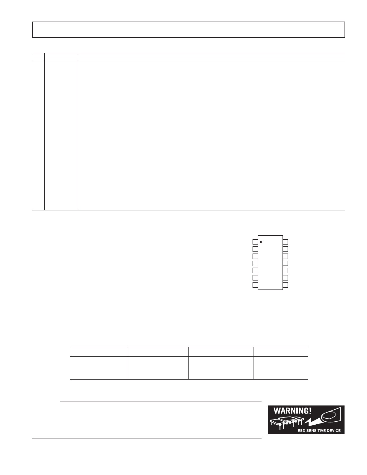
range of 0°C to 70°C, and is available in a 14-lead SOIC package.
REV. A
Information furnished by Analog Devices is believed to be accurate and
reliable. However, no responsibility is assumed by Analog Devices for its
use, nor for any infringements of patents or other rights of third parties that
may result from its use. No license is granted by implication or otherwise
under any patent or patent rights of Analog Devices. Trademarks and
registered trademarks are the property of their respective owners.
One Technology Way, P.O. Box 9106, Norwood, MA 02062-9106, U.S.A.
Tel: 781/329-4700 www.analog.com
Fax: 781/326-8703 © 2005 Analog Devices, Inc. All rights reserved.

ADP3171–SPECIFICATIONS
Parameter Symbol Conditions Min Typ Max Unit
FEEDBACK INPUT
Output Accuracy V
Line Regulation ∆V
Crowbar Trip Point V
Crowbar Reset Point % of Nominal FB Voltage 40 50 60 %
Crowbar Response Time t
OSCILLATOR
Off Time T
CT Charge Current I
ERROR AMPLIFIER
Output Resistance R
Transconductance g
Output Current I
Maximum Output Voltage V
Output Disable Threshold V
–3 dB Bandwidth BW
CURRENT SENSE
Threshold Voltage V
Input Bias Current I
Response Time t
OUTPUT DRIVERS
Output Resistance R
Output Transition Time tR, t
LINEAR REGULATORS
Feedback Current I
LR1 Feedback Voltage V
LR2 Feedback Voltage V
Driver Output Voltage V
POWER GOOD COMPARATOR
Undervoltage Threshold V
Undervoltage Hysteresis % of Nominal FB Voltage 5 %
Overvoltage Threshold V
Overvoltage Reset Point % of Nominal FB Voltage 40 50 60 %
Output Voltage Low V
Response Time 250 ns
SUPPLY
DC Supply Current
2
UVLO Threshold Voltage V
UVLO Hysteresis 0.8 1 1.2 V
NOTES
1
All limits at temperature extremes are guaranteed via correlation using standard Statistical Quality Control (SQC).
2
Dynamic supply current is higher due to the gate charge being delivered to the external MOSFETs.
Specifications subject to change without notice.
FB
OUT
CROWBAR
CROWBAR
CT
O(ERR)
m(ERR)
O(ERR)
COMP(MAX)
COMP(OFF)
ERR
CS(TH)
, I
CS+
CS
O(DRV(X))IL
F
LRFB(X)
LRFB(1)
LRFB(2)
LRDRV(X)
PWRGD(UV)
PWRGD(OV)
OL(PWRGD)IPWRGD(SINK)
I
CC
UVLO
(VCC = 12 V, TA = 0C to 70C, unless otherwise noted.)
Figure 1 1.188 1.2 1.212 V
VCC = 10 V to 14 V 0.06 %
% of Nominal FB Voltage 115 120 125 %
Overvoltage to DRVL Going High 400 ns
= 25°C, CT = 200 pF 3.5 4 4.5 µs
A
TA = 25°C, V
TA = 25°C, V
FB Forced to V
FB Forced to V
in Regulation 130 150 170 µA
OUT
= 0 V 253545 µA
OUT
– 3% 625 µA
OUT
– 3% 3.0 V
OUT
COMP = Open 500 kHz
FB Forced to V
– 3% 69 78 87 mV
OUT
FB ≤ 0.45 V 35 45 54 mV
0.8 V ≤ COMP ≤ 1 V 1 5 mV
CS–
CS+ = CS– = V
OUT
CS+ – (CS–) > 87 mV 50 ns
to DRVH Going Low
= 50 mA 6 Ω
CL = 3000 pF 80 ns
Figure 2, VCC = 4.5 V to 12.6 V 1.45 1.5 1.55 V
Figure 2, VCC = 4.5 V to 12.6 V 1.75 1.8 1.85 V
VCC = 4.5 V, V
= 0 V 4.2 V
LRFB(X)
% of Nominal FB Voltage 75 80 85 %
% of Nominal FB Voltage 115 120 125 %
= 1 mA 250 500 mV
130 kΩ
2.05 2.2 2.35 mmho
600 750 900 mV
0.5 5 µA
0.3 1 µA
79 mA
6.75 7 7.25 V
1
REV. A–2–

ADP3171
TOP VIEW
(Not to Scale)
14
1
5
PWRGD
LRFB1
LRDRV1
FB
CS–
CS+
DRVH
DRVL
VCC
LRFB2
LRDRV2
COMP
CT
GND
ADP3171
3
2
4
7
13
12
11
10
9
8
6
PIN FUNCTION DESCRIPTIONS
Pin Mnemonic Function
1 GND Ground Reference. GND should have a low impedance path to the source of the synchronous MOSFET.
2 PWRGD Power Good Indicator. Open-drain output that signals when the output voltage is in the proper operating range.
3, 11
LRFB1, Feedback connections for the fixed output voltage linear regulator controllers.
LRFB2
4, 10
LRDRV1, Gate drives for the respective linear regulator N-channel MOSFETs.
LRDRV2
5FB Feedback Input. Error amplifier input for remote sensing of the output voltage.
6 CS– Current Sense Negative Node. Negative input for the current comparator.
7 CS+ Current Sense Positive Node. Positive input for the current comparator. The output current is sensed as a voltage
at this pin with respect to CS–.
8CT Timing Capacitor. An external capacitor connected from CT to ground sets the off time of the device.
9 COMP Error Amplifier Output and Compensation Point. The voltage at this output programs the output current control
level between CS+ and CS–.
12 VCC Supply Voltage for the ADP3171.
13 DRVL Low-Side MOSFET Drive. Gate drive for the synchronous rectifier N-channel MOSFET. The voltage at DRVL
swings from GND to VCC.
14 DRVH High-Side MOSFET Drive. Gate drive for the buck switch N-channel MOSFET. The voltage at DRVH swings
from GND to VCC.
ABSOLUTE MAXIMUM RATINGS*
VCC . . . . . . . . . . . . . . . . . . . . . . . . . . . . . . . –0.3 V to +15 V
DRVH, DRVL, LRDRV1, LRDRV2 . . . . . . –0.3 V to VCC + 0.3 V
All Other Inputs and Outputs . . . . . . . . . . . . –0.3 V to +10 V
Operating Ambient Temperature Range . . . . . . . 0°C to 70°C
Operating Junction Temperature . . . . . . . . . . . . . . . . . . 125°C
Storage Temperature Range . . . . . . . . . . . . –65°C to +150°C
. . . . . . . . . . . . . . . . . . . . . . . . . . . . . . . . . . . . . . . 105°C/W
JA
Lead Temperature (Soldering, 10 sec) . . . . . . . . . . . . . 300°C
Vapor Phase (60 sec) . . . . . . . . . . . . . . . . . . . . . . . . . . . 215°C
Infrared (15 sec) . . . . . . . . . . . . . . . . . . . . . . . . . . . . . . 220°C
*Stresses above those listed under Absolute Maximum Ratings may cause perma-
nent damage to the device. This is a stress rating only; functional operation of the
device at these or any other conditions above those listed in the operational
sections of this specification is not implied. Exposure to absolute maximum rating
conditions for extended periods may affect device reliability. Unless otherwise
specified, all voltages are referenced to GND.
ORDERING GUIDE
Model Temperature Range Package Description Package Option
ADP3171JR 0ºC to 70ºC 14-Lead Narrow SOIC R-14
ADP3171JR-REEL 0ºC to 70ºC 14-Lead Narrow SOIC R-14
ADP3171JR-REEL7 0ºC to 70ºC 14-Lead Narrow SOIC R-14
PIN CONFIGURATION
CAUTION
ESD (electrostatic discharge) sensitive device. Electrostatic charges as high as 4000 V readily
accumulate on the human body and test equipment and can discharge without detection. Although the
ADP3171 features proprietary ESD protection circuitry, permanent damage may occur on devices
–3–
subjected to high energy electrostatic discharges. Therefore, proper ESD precautions are recommended
to avoid performance degradation or loss of functionality.
REV. A

ADP3171–Typical Performance Characteristics
60
50
40
30
20
SUPPLY CURRENT – mA
10
2
0
0 200 400 600 800
OSCILLATOR FREQUENCY – kHz
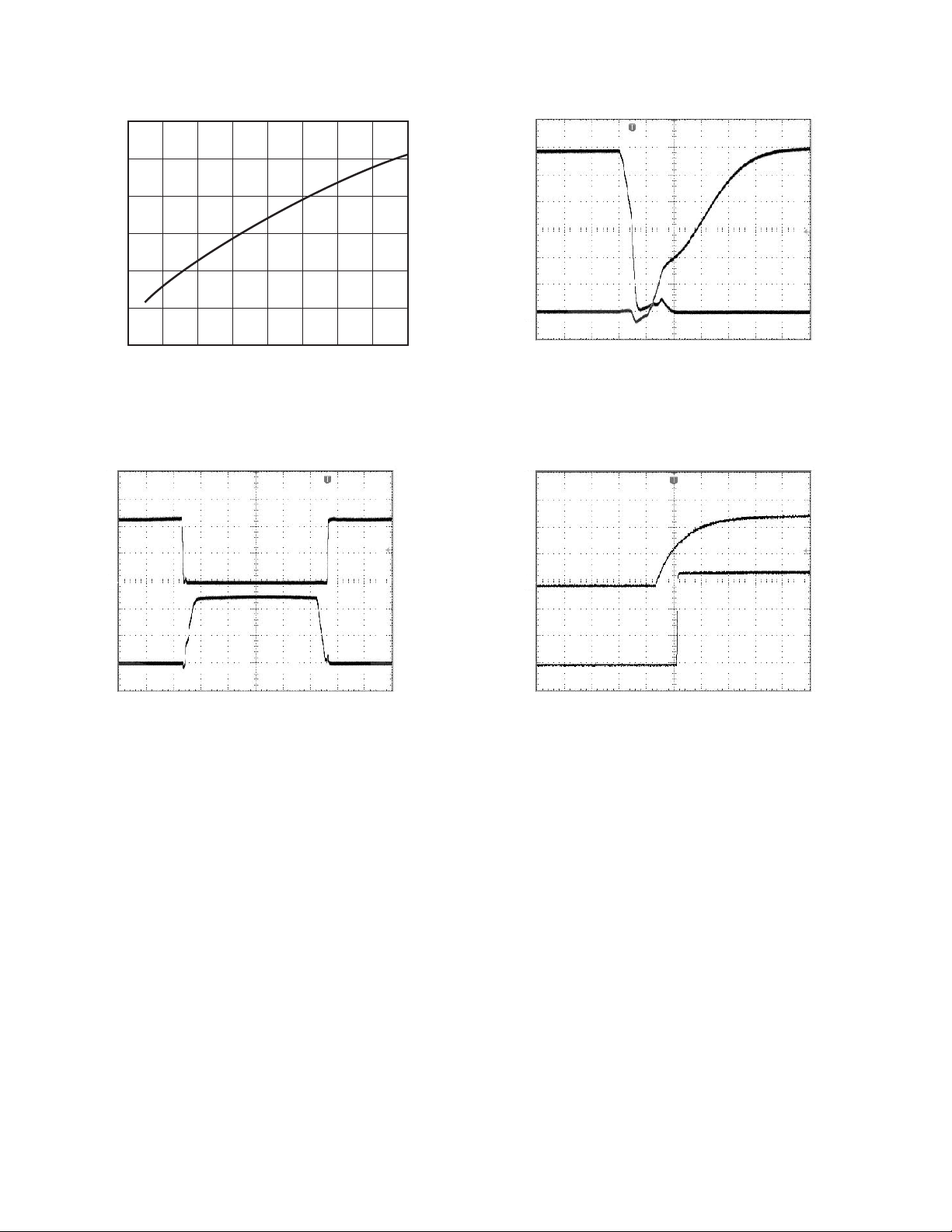
TPC 1. Supply Current vs. Operating Frequency
Using MOSFETs of Figure 3
1
2
CH1 = 5.0V CH2 = 5.0V
M = 1.0sA: CH1 = 5.9V
TPC 2. Gate Switching Waveforms Using
MOSFETs of Figure 3
CH1 = 2.0V CH2 = 2.0V
M = 100ns A: CH1 = 5.88V
TPC 3. Driver Transition Waveforms Using
MOSFETs of Figure 3
1
2
CH1 = 5.0V CH2 = 500mV
M = 10.0ms A: CH1 = 5.9V
TPC 4. Power-On Start-Up Waveform
REV. A–4–
 Loading...