Analog Devices ADP3170JRU Datasheet

VRM 8.5 Compatible
a
FEATURES
Optimally Compensated Active Voltage Positioning
with Gain and Offset Adjustment (ADOPT™) for
Superior Load Transient Response
Complies with VRM 8.5 Specifications with Lowest
System Cost
5-Bit Digitally Programmable 1.05 V to 1.825 V Output
N-Channel Synchronous Buck Controller
Onboard 1.8 V Linear Regulator Controller
Total Accuracy 1% Over Temperature
High Efficiency Current-Mode Operation
Short Circuit Protection
Power Good Output
Overvoltage Protection Crowbar Protects
Microprocessors with No Additional External
Components
APPLICATIONS
Core and 1.8 V Standby Supplies for Next Generation
Intel Pentium® III Processors
Single Phase Core Controller
ADP3170
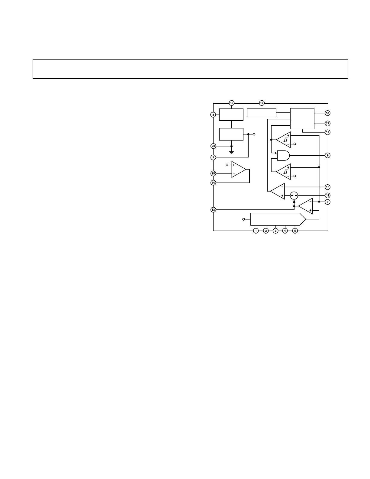
FUNCTIONAL BLOCK DIAGRAM
SD
GND
REF
LRFB
LRDRV
COMP
VCC
UVLO
AND BIAS
3.0V
REFERENCE
1.8V
ADP3170
REF
CT
OSCILLATOR
REF
SET
RESET
CROWBAR
CMP
VID
DAC
PWM
LOGIC
DAC +20%
DAC –20%
g
m
DRVH
DRVL
PGND
PWRGD
CS–
CS+
FB
GENERAL DESCRIPTION
The ADP3170 is a highly efficient output synchronous buck
switching regulator controller optimized for converting a 5 V
main supply into the core supply voltage required by next
generation Intel Celeron processors. The ADP3170 uses an
internal 5-bit DAC to read a voltage identification (VID)
code directly from the processor, which is used to set the
output voltage between 1.05 V and 1.825 V. The ADP3170
uses a current mode, constant off-time architecture to drive two
N-channel MOSFETs at a programmable switching frequency
that can be optimized for regulator size and efficiency.
The ADP3170 also uses a unique supplemental regulation technique called Analog Devices Optimal Positioning Technology
(ADOPT) to enhance load transient performance. Active
voltage positioning results in a dc/dc converter that meets the
stringent output voltage specifications for high performance
processors, with the minimum number of output capacitors and
smallest footprint. Unlike voltage-mode and standard current-
ADOPT is a trademark of Analog Devices, Inc.
Pentium is a registered trademark of Intel Corporation
VID25VID0VID1VID2VID3
mode architectures, active voltage positioning adjusts the output
voltage as a function of the load current so that it is always
optimally positioned for a system transient. The ADP3170 also
provides accurate and reliable short circuit protection and
adjustable current limiting. It also includes an integrated
overvoltage crowbar function to protect the microprocessor
from destruction in case the core supply exceeds the nominal
programmed voltage by more than 20%.
The ADP3170 contains a 1.8 V linear regulator controller that
is designed to drive an external N-channel MOSFET. This linear
regulator can be used to generate auxiliary voltages (such as 1.8 V
standby power) required in most motherboard designs, and has
been designed to provide a high bandwidth load-transient response.
The ADP3170 is specified over the commercial temperature range
of 0°C to 70°C and is available in a 20-lead TSSOP package.
REV. 0
Information furnished by Analog Devices is believed to be accurate and
reliable. However, no responsibility is assumed by Analog Devices for its
use, nor for any infringements of patents or other rights of third parties that
may result from its use. No license is granted by implication or otherwise
under any patent or patent rights of Analog Devices.
One Technology Way, P.O. Box 9106, Norwood, MA 02062-9106, U.S.A.
Tel: 781/329-4700 www.analog.com
Fax: 781/326-8703 © Analog Devices, Inc., 2001

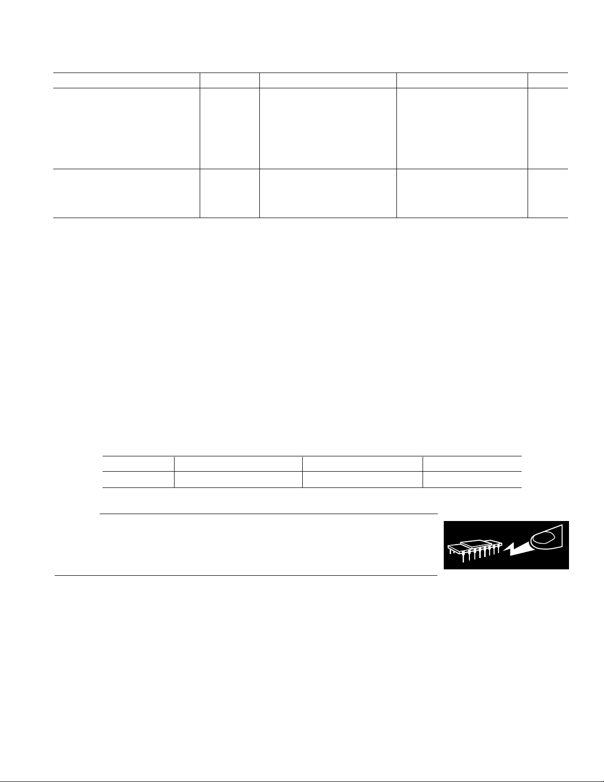
ADP3170–SPECIFICA TIONS
Parameter Symbol Conditions Min Typ Max Unit
FEEDBACK INPUT
Output Accuracy V
1.05 V Output Figure 1 1.039 1.05 1.061 V
1.5 V Output Figure 1 1.485 1.5 1.515 V
1.825 V Output Figure 1 1.807 1.825 1.843 V
Line Regulation ∆V
Input Bias Current I
Crowbar Trip Point V
Crowbar Reset Point % of Nominal DAC Voltage 40 50 60 %
Crowbar Response Time t
REFERENCE
Output Voltage V
Output Current I
VID INPUTS
Input Low Voltage V
Input High Voltage V
Input Current I
Pull-up Resistance R
Internal Pull-up Voltage 2.75 3.1 3.4 V
SHUTDOWN INPUT
Input Low Voltage V
Input High Voltage V
Input Current I
OSCILLATOR
Off Time T
CT Charge Current I
ERROR AMPLIFIER
Output Resistance R
Transconductance g
Output Current I
Maximum Output Voltage V
Output Disable Threshold V
–3 dB Bandwidth BW
CURRENT SENSE
Threshold Voltage V
Input Bias Current I
Response Time t
OUTPUT DRIVERS
Output Resistance R
Output Transition Time tR, t
LINEAR REGULATOR
Feedback Current I
LR Feedback Voltage V
Driver Output Voltage V
FB
OUT
FB
CROWBAR
CROWBAR
REF
REF
IL(VID)
IH(VID)
VID
VID
IL(SD)
IH(SD)
SD
CT
O(ERR)
m(ERR)
O(ERR)
COMP(MAX)
COMP(OFF)
ERR
CS(TH)
, I
CS+
CS–
CS
O(DRV[X])
F
LRFB
LRFB
LRDRV
(VCC = 12 V, I
= 150 A, TA = 0C to 70C, unless otherwise noted.)
REF
VCC = 10 V to 14 V 0.06 %
550nA
% of Nominal DAC Voltage 115 120 125 %
Overvoltage to DRVL Going High 400 ns
2.937 3.0 3.048 V
300 µA
0.8 V
2.3 V
VID(X) = 0 V 300 425 µA
16 kΩ
0.8 V
2.0 V
1 µA
= 25°C, CT = 200 pF 3.5 4.0 4.5 µs
A
T
= 25°C, V
A
T
= 25°C, V
A
in Regulation 130 150 170 µA
OUT
= 0 V 25 35 45 µA
OUT
1MΩ
2.05 2.2 2.35 mmho
FB = 0 625 µA
FB Forced to V
– 3% 3.0 V
OUT
600 750 900 mV
COMP = Open 500 kHz
FB Forced to V
– 3% 69 78 87 mV
OUT
FB ≤ 0.45 V 35 45 54 mV
0.8 V ≤ COMP ≤ 1 V 1 5 mV
CS+ = CS– = V
OUT
0.5 5 µA
CS+ – (CS–) > 87 mV 50 ns
to DRVH going low
I
= 50 mA 4.5 Ω
L
CL = 3000 pF 75 ns
0.3 1 µA
Figure 2, VCC = 4.5 V to 12.6 V 1.75 1.8 1.85 V
VCC = 4.5 V, V
= 0 V 4.2 V
LRFB(X)
1
–2–
REV. 0

ADP3170
Parameter Symbol Conditions Min Typ Max Unit
POWER GOOD COMPARATOR
Undervoltage Threshold V
PWRGD(UV)
Undervoltage Hysteresis % of Nominal DAC Voltage 5 %
Overvoltage Threshold V
PWRGD(OV)
Overvoltage Reset Point % of Nominal DAC Voltage 40 50 60 %
Output Voltage Low V
OL(PWRGD)IPWRGD(SINK)
Response Time 200 ns
SUPPLY
DC Supply Current
UVLO Threshold Voltage V
2
I
CC
UVLO
UVLO Hysteresis 0.8 1 1.2 V
NOTES
1
All limits at temperature extremes are guaranteed via correlation using standard Statistical Quality Control (SQC).
2
Dynamic supply current is higher due to the gate charge being delivered to the external MOSFETs.
Specifications subject to change without notice.
ABSOLUTE MAXIMUM RATINGS*
VCC . . . . . . . . . . . . . . . . . . . . . . . . . . . . . . . –0.3 V to +15 V
DRVH, DRVL, LRDRV . . . . . . . . . . –0.3 V to VCC + 0.3 V
All Other Inputs & Outputs . . . . . . . . . . . . . . –0.3 V to +10 V
Operating Ambient Temperature Range . . . . . . . 0°C to 70°C
Operating Junction Temperature . . . . . . . . . . . . . . . . . 125°C
Storage Temperature Range . . . . . . . . . . . . –65°C to +150°C
. . . . . . . . . . . . . . . . . . . . . . . . . . . . . . . . . . . . . . 143°C/W
JA
Lead Temperature (Soldering, 10 sec) . . . . . . . . . . . . 300°C
Vapor Phase (60 sec) . . . . . . . . . . . . . . . . . . . . . . . . . . 215°C
Infrared (15 sec) . . . . . . . . . . . . . . . . . . . . . . . . . . . . . 220°C
*This is a stress rating only; operation beyond these limits can cause the device to
be permanently damaged. Unless otherwise specified, all voltages are referenced
to GND.
% of Nominal DAC Voltage 74 80 86 %
% of Nominal DAC Voltage 114 120 126 %
= 1 mA 250 500 mV
7.5 9.5 mA
6.75 7 7.25 V
ORDERING GUIDE
Model Temperature Range Package Description Package Option
ADP3170JRU 0°C to 70°C TSSOP RU-20
CAUTION
ESD (electrostatic discharge) sensitive device. Electrostatic charges as high as 4000 V readily
accumulate on the human body and test equipment and can discharge without detection. Although
the ADP3170 features proprietary ESD protection circuitry, permanent damage may occur on
devices subjected to high-energy electrostatic discharges. Therefore, proper ESD precautions are
recommended to avoid performance degradation or loss of functionality.
WARNING!
ESD SENSITIVE DEVICE
REV. 0
–3–

ADP3170
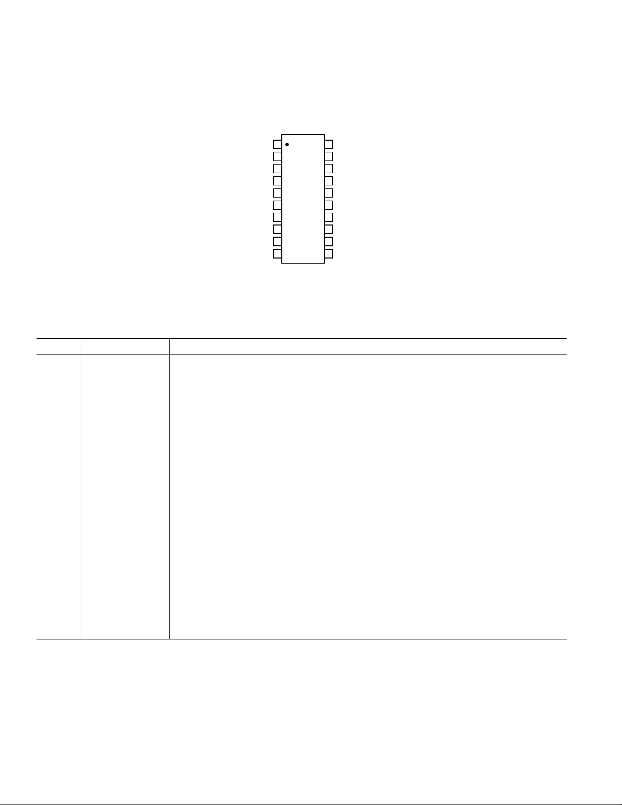
PIN CONFIGURATION
RU-20
VID3
VID2
VID1
VID0
VID25
PWRGD
REF
CS–
SD
FB
10
1
2
3
4
5
ADP3170
TOP VIEW
6
(Not to Scale)
7
8
9
20
19
18
17
16
15
14
13
12
11
GND
PGND
DRVH
DRVL
VCC
LRFB
LRDRV
COMP
CT
CS+
PIN FUNCTION DESCRIPTIONS
Pin No. Mnemonic Function
1–5 VID3, VID2, Voltage Identification DAC Inputs. These pins are pulled up to an internal reference,
VID1, VID0, providing a logic one if left open. The DAC output programs the FB regulation voltage from
VID25 1.05 V to 1.825 V.
6 PWRGD Open drain output that signals when the output voltage is in the proper operating range.
7 REF 3.0 V Reference Output.
8 SD Regulator Shutdown. Pulling this pin high turns off both MOSFETs of the switching
regulator. SD has no effect on the linear regulator controller.
9 FB Feedback Input. Error amplifier input for remote sensing of the output voltage.
10 CS– Current Sense Negative Node. Negative input for the current comparator.
11 CS+ Current Sense Positive Node. Positive input for the current comparator. The output current is
sensed as a voltage at this pin with respect to CS–.
12 CT External capacitor connected from CT to ground sets the OFF-Time of the device.
13 COMP Error Amplifier Output and Compensation Point. The voltage at this output programs the
output current control level between CS+ and CS–.
14 LRDRV Gate Drive for the 1.8 V linear regulator N-channel MOSFET.
15 LRFB Feedback Connections for the 1.8 V linear regulator controller.
16 VCC Supply Voltage for the ADP3170.
17 DRVL Low-Side MOSFET Drive. Gate drive for the synchronous rectifier N-channel MOSFET.
The voltage at DRVL swings from GND to VCC.
18 DRVH High-Side MOSFET Drive. Gate drive for the buck switch N-channel MOSFET. The voltage
at DRVH swings from GND to VCC.
19 PGND Power Ground. PGND should have a low impedance path to the source of the synchronous
MOSFET.
20 GND Small-Signal Ground. This ground reference can be used in conjunction with FB to provide
remote sensing of the output voltage at the CPU pins.
–4–
REV. 0

5-BIT CODE
V
FB
1
2
3
4
5
6
7
8
9
10
ADP3170
VID3
VID2
VID1
VID0
VID25
PWRGD
REF
SD
FB
CS–
GND
PGND
DRVH
DRVL
VCC
LRFB
LRDRV
COMP
CS+
ADP3170
20
19
18
17
16
1F
15
14
13
12
CT
11
12V
100nF
100
100nF
AD820
1.2V
1
2
3
4
5
6
7
8
9
10
ADP3170
VID3
VID2
VID1
VID0
VID25
PWRGD
REF
SD
FB
CS–
GND
PGND
DRVH
DRVL
VCC
LRFB
LRDRV
COMP
CS+
20
19
18
17
16
15
14
13
12
CT
11
1F
10nF
100nF
VCC
V
LR
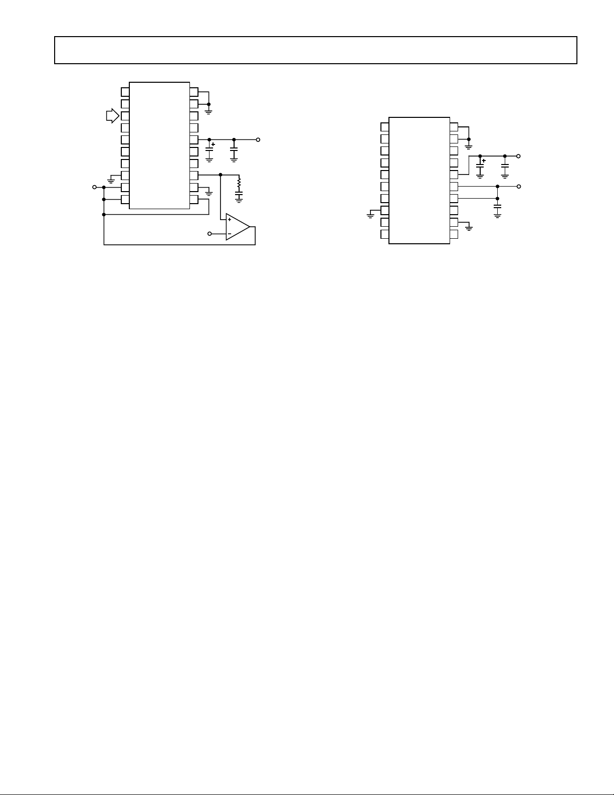
Figure 1. Closed-Loop Output Voltage Accuracy
Test Circuit
Figure 2. Linear Regulator Output Voltage Accuracy
Test Circuit
REV. 0
–5–
 Loading...