

查询ADP3167供应商
5-Bit Programmable 2-Phase
a
FEATURES
ADOPT™ Optimal Positioning Technology for Superior
Load Transient Response and Fewest Output Capacitors
Complies with VRM 9.0 with Lowest System Cost
Active Current Balancing between Both Output Phases
5-Bit Digitally Programmable 1.1 V to 1.85 V Output
Dual Logic-Level PWM Outputs for Interface to External
High Power Drivers
Total Output Accuracy ⴞ0.8% over Temperature
Current-Mode Operation
Short Circuit Protection
Power Good Output
Overvoltage Protection Crowbar Protects
Microprocessors with No Additional
External Components
APPLICATIONS
Desktop PC Power Supplies for:
Intel Pentium
AMD Athlon™ Processors
VRM Modules
®
4 Processors
Synchronous Buck Controller
ADP3160/ADP3167
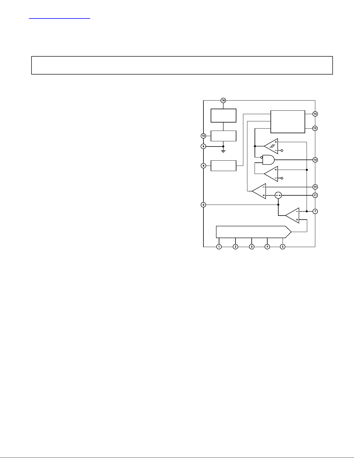
FUNCTIONAL BLOCK DIAGRAM
VCC
CROWBAR
CMP1
SET
RESET
CMP3
CMP2
CMP
CMP
2-PHASE
DRIVER
LOGIC
DAC+24%
DAC–18%
g
m
REF
GND
CT
COMP
UVLO
AND
BIAS
3.0V
REFERENCE
OSCILLATOR
ADP3160/ADP3167
PWM1
PWM2
PWRGD
CS–
CS+
FB
GENERAL DESCRIPTION
The ADP3160 and ADP3167 are highly efficient, dual output,
synchronous buck switching regulator controllers optimized for
converting a 5 V or 12 V main supply into the core supply voltage
required by high-performance processors, such as Pentium 4 and
Athlon. The ADP3160 uses an internal 5-bit DAC to read a voltage identification (VID) code directly from the processor that is
used to set the output voltage between 1.1 V and 1.85 V. The
devices use a current-mode PWM architecture to drive two logiclevel outputs at a programmable switching frequency that can be
optimized for VRM size and efficiency. The output signals are
180 degrees out of phase, allowing for the construction of two
complementary buck switching stages. These two stages share the
dc output current to reduce overall output voltage ripple. An
active current balancing function ensures that both phases carry
equal portions of the total load current, even under large transient
loads, to minimize the size of the inductors. The ADP3160 control
ADOPT is a trademark of Analog Devices, Inc.
Athlon is a trademark of Advanced Micro Devices, Inc.
Pentium is a registered trademark of Intel Corporation.
VID
DAC
VID4 VID3 VID2 VID1 VID0
loop has been optimized for conversion from 12 V, while the
ADP3167 is designed for conversion from a 5 V supply.
The ADP3160 and ADP3167 also use a unique supplemental
regulation technique called active voltage positioning to enhance
load transient performance. Active voltage positioning results
in a dc/dc converter that meets the stringent output voltage
specifications for high-performance processors, with the minimum
number of output capacitors and smallest footprint. Unlike
voltage-mode and standard current-mode architectures, active
voltage positioning adjusts the output voltage as a function of
the load current so that it is always optimally positioned for a
system transient. They also provide accurate and reliable short
circuit protection and adjustable current limiting.
The ADP3160 is specified over the commercial temperature
range of 0∞C to 70∞C and is available in a 16-lead narrow body
SOIC package.
REV.B
Information furnished by Analog Devices is believed to be accurate and
reliable. However, no responsibility is assumed by Analog Devices for its
use, nor for any infringements of patents or other rights of third parties that
may result from its use. No license is granted by implication or otherwise
under any patent or patent rights of Analog Devices.
One Technology Way, P.O. Box 9106, Norwood, MA 02062-9106, U.S.A.
Tel: 781/329-4700www.analog.com
Fax: 781/326-8703 © Analog Devices, Inc., 2002

ADP3160/ADP3167–SPECIFICATIONS
(VCC = 12 V, I
1
unless otherwise noted.)
= 150 A, TA = 0ⴗC to 70ⴗC,
REF
Parameter Symbol Conditions Min Typ Max Unit
FEEDBACK INPUT
Accuracy V
FB
1.1 V Output See Figure 1 1.091 1.1 1.109 V
1.475 V Output See Figure 1 1.463 1.475 1.487 V
1.85 V Output See Figure 1 1.835 1.85 1.865 V
Line Regulation ⌬V
Input Bias Current I
FB
Crowbar Trip Threshold V
FB
CROWBAR
VCC = 10 V to 14 V 0.05 %
550 nA
Percent of Nominal Output 114 124 134 %
Crowbar Reset Threshold Percent of Nominal Output 50 60 70 %
Crowbar Response Time t
CROWBAR
Overvoltage to PWM Going Low 300 ns
REFERENCE
Output Voltage V
Output Current I
REF
REF
2.952 3.0 3.048 V
300 mA
VID INPUTS
Input Low Voltage V
Input High Voltage V
Input Current I
Pull-Up Resistance R
IL(VID)
IH(VID)
VID
VID
2.2 V
VID(X) = 0 V 180 250 mA
20 28 kW
0.6 V
Internal Pull-Up Voltage 4.5 5.0 5.5 V
OSCILLATOR
Maximum Frequency
Frequency Variation ⌬f
CT Charge Current I
2
f
CT(MAX)
CT
CT
2000 kHz
TA = 25∞C, CT = 91 pF 430 500 570 kHz
TA = 25∞C, VFB in Regulation 130 150 170 mA
TA = 25∞C, VFB = 0 V 263646 mA
ERROR AMPLIFIER
Output Resistance R
Transconductance g
Output Current I
Maximum Output Voltage V
Output Disable Threshold V
O(ERR)
m(ERR)
O(ERR)
COMP(MAX)
COMP(OFF)
2.0 2.2 2.45 mmho
VFB = 0 V 1 mA
FB Forced to V
– 3% 3.0 V
OUT
ADP3160 560 720 800 mV
200 kW
ADP3167 640 800 880 mV
–3 dB Bandwidth BW
ERR
COMP = Open 500 kHz
CURRENT SENSE
Current Limit Threshold Voltage V
CS(CL)
ADP3160, CS+ = VCC 142 157 172 mV
FB Forced to V
OUT
– 3%
ADP3167, CS+ = VCC 69 79 89 mV
FB Forced to V
OUT
– 3%
0.8 V £ COMP £ 1 V 0 15 mV
Current Limit Foldback Voltage V
CS(FOLD)
ADP3160, FB £ 375 mV 75 95 115 mV
ADP3167, FB £ 750 mV 37 47 58 mV
COMP
/DV
CS
DV
Input Bias Current I
Response Time t
n
I
CS+
CS
, I
CS–
ADP3160, 1 V £ V
ADP3167, 1 V £ V
£ 3 V 12.5 V/V
COMP
£ 3 V 25 V/V
COMP
CS+ = CS– = VCC 0.5 5 mA
ADP3160, CS+ – (CS–) ≥ 172 mV 50 ns
to PWM Going Low
ADP3167, CS+ – (CS–) ≥ 89 mV 50 ns
to PWM Going Low
POWER GOOD COMPARATOR
Undervoltage Threshold V
Overvoltage Threshold V
Output Voltage Low V
PWRGD(UV)
PWRGD(OV)
OL(PWRGD)IPWRGD(SINK)
% Nominal Output 76 82 88 %
% Nominal Output 114 124 134 %
= 100 mA30200 mV
Response Time FB Going High 2 ms
FB Going Low 200 ns
REV. B–2–

ADP3160/ADP3167
Parameter Symbol Conditions Min Typ Max Unit
PWM OUTPUTS
Output Voltage Low V
Output Voltage High V
Output Current I
Duty Cycle Limit
2
OL(PWM)
OH(PWM)
PWM
D
MAX
SUPPLY
DC Supply Current
Normal Mode I
UVLO Mode I
UVLO Threshold Voltage V
CC
CC(UVLO)
UVLO
UVLO Hysteresis 0.1 0.4 0.6 V
NOTES
1
All limits at temperature extremes are guaranteed via correlation using standard Statistical Quality Control (SQC) methods.
2
Guaranteed by design, not tested in production.
Specifications subject to change without notice.
I
PWM(SINK)
I
PWM(SOURCE)
= 400 mA 100 500 mV
= 400 mA 4.0 V
Per Phase, Relative to f
VCC £ V
, VCC Rising 220 400 mA
UVLO
CT
0.4 1 mA
50 %
3.8 5.5 mA
5.9 6.4 6.9 V
REV. B
–3–
ADP3160/ADP3167
WARNING!
ESD SENSITIVE DEVICE
ABSOLUTE MAXIMUM RATINGS*
VCC . . . . . . . . . . . . . . . . . . . . . . . . . . . . . . –0.3 V to +15 V
CS+, CS– . . . . . . . . . . . . . . . . . . . . . . –0.3 V to VCC + 0.3 V
All Other Inputs and Outputs . . . . . . . . . . . . –0.3 V to +10 V
Operating Ambient Temperature Range . . . . . . . 0∞C to 70∞C
Operating Junction Temperature . . . . . . . . . . . . . . . . . . 125∞C
Storage Temperature Range . . . . . . . . . . . . –65∞C to +150∞C
JA
Two-Layer Board . . . . . . . . . . . . . . . . . . . . . . . . . . 125∞C/W
Four-Layer Board . . . . . . . . . . . . . . . . . . . . . . . . . . 81∞C/W
Lead Temperature (Soldering, 10 sec) . . . . . . . . . . . . . 300∞C
Vapor Phase (60 sec) . . . . . . . . . . . . . . . . . . . . . . . . . . . 215∞C
Infrared (15 sec) . . . . . . . . . . . . . . . . . . . . . . . . . . . . . . 220∞C
*This is a stress rating only; operation beyond these limits can cause the device to
be permanently damaged. Unless otherwise specified, all voltages are referenced
to GND.
PIN CONFIGURATION
VID4
VID3
VID2
VID1
VID0
COMP
FB
CT
1
2
3
ADP3160/
ADP3167
4
TOP VIEW
5
(Not to Scale)
6
7
8
16
15
14
13
12
11
10
9
VCC
REF
CS–
PWM1
PWM2
CS+
PWRGD
GND
PIN FUNCTION DESCRIPTIONS
Pin Mnemonic Function
1–5 VID4– Voltage Identification DAC Inputs.
VID0 These pins are pulled up to an internal
reference, providing a Logic 1 if left open.
The DAC output programs the FB regulation voltage from 1.1 V to 1.85 V. Leaving
all five DAC inputs open results in the
ADP3160/ADP3167 going into a “No
CPU” mode, shutting off its PWM outputs.
6 COMP Error Amplifier Output and Compensation
Point. The voltage at this output programs
the output current control level between
CS+ and CS–.
7FB Feedback Input. Error amplifier input for
remote sensing of the output voltage.
8CT External Capacitor CT Connection to
ground sets the frequency of the device.
9GND Ground. All internal signals of the ADP3160/
ADP3167 are referenced to this ground.
10 PWRGD Open-Drain Output that signals when the
output voltage is in the proper operating range.
11 CS+ Current Sense Positive Node. Positive input
for the current comparator. The output
current is sensed as a voltage at this pin with
respect to CS–.
12 PWM2 Logic-Level Output for Phase 2 Driver
13 PWM1 Logic-Level Output for Phase 1 Driver
14 CS– Current Sense Negative Node. Negative
input for the current comparator.
15 REF 3.0 V Reference Output
16 VCC Supply Voltage for the ADP3160/ADP3167.
ORDERING GUIDE
Temperature Package
Model Range Description Package Option
ADP3160JR 0∞C to 70∞CNarrow Body SOIC R-16A (SO-16)
ADP3167JR 0∞C to 70∞CNarrow Body SOIC R-16A (SO-16)
CAUTION
ESD (electrostatic discharge) sensitive device. Electrostatic charges as high as 4000 V readily
accumulate on the human body and test equipment and can discharge without detection. Although the
ADP3160/ADP3167 features proprietary ESD protection circuitry, permanent damage may occur on
devices subjected to high-energy electrostatic discharges. Therefore, proper ESD precautions are
recommended to avoid performance degradation or loss of functionality.
REV. B–4–
ADP3160/ADP3167
ADP3160/ADP3167
VCC
REF
CS–
PWM1
PWM2
CS+
PWRGD
GND
16
15
14
13
12
11
10
1.2V
+
1F
20k⍀
9
5-BIT CODE
100⍀
100nF
1
2
3
4
5
6
7
8
AD820
VID4
VID3
VID2
VID1
VID0
COMP
FB
CT
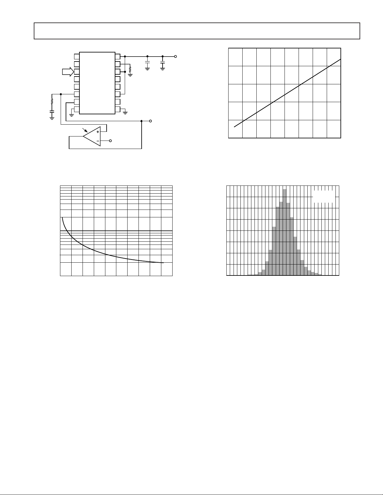
Figure 1. Closed-Loop Output Voltage Accuracy
Test Circuit
10000
4.10
12V
100nF
V
FB
4.05
4.00
3.95
SUPPLY CURRENT – mA
3.90
3.85
0 2000
250 500 750 1250 1500 1750
OSCILLATOR FREQUENCY – kHz
1000
Figure 3. Supply Current vs. Oscillator Frequency
16
TA = 25ⴗC
= 1.6V
V
OUT
12
1000
OSCILLATOR FREQUENCY – kHz
100
0
100
200 300 400 500
CT CAPACITOR – pF
Figure 2. Oscillator Frequency vs. Timing Capacitor
8
NUMBER OF PARTS – %
4
0
–1 1
OUTPUT ACCURACY – % of Nominal
0
Figure 4. Output Accuracy Distribution
REV. B
–5–
ADP3160/ADP3167
THEORY OF OPERATION
The ADP3160 and ADP3167 combine a current-mode, fixed
frequency PWM controller with antiphase logic outputs in a
controller for a 2-phase synchronous buck power converter.
Two-phase operation is important for switching the high currents
required by high-performance microprocessors. Handling the
high current in a single-phase converter would place difficult
requirements on the power components such as inductor wire
size, MOSFET ON resistance, and thermal dissipation. Their
high-side current sensing topology ensures that the load currents
are balanced in each phase, such that neither phase has to carry
more than half of the power. An additional benefit of high-
side
current sensing over output current sensing is that the average
current through the sense resistor is reduced by the duty cycle
of the converter, allowing the use of a lower power, lower cost
resistor. The outputs of the ADP3160/ADP3167 are logic
drivers only and are not intended to drive external power
MOSFETs directly. Instead, the ADP3160/ADP3167
be paired with drivers such as the ADP3414 or ADP3417.
should
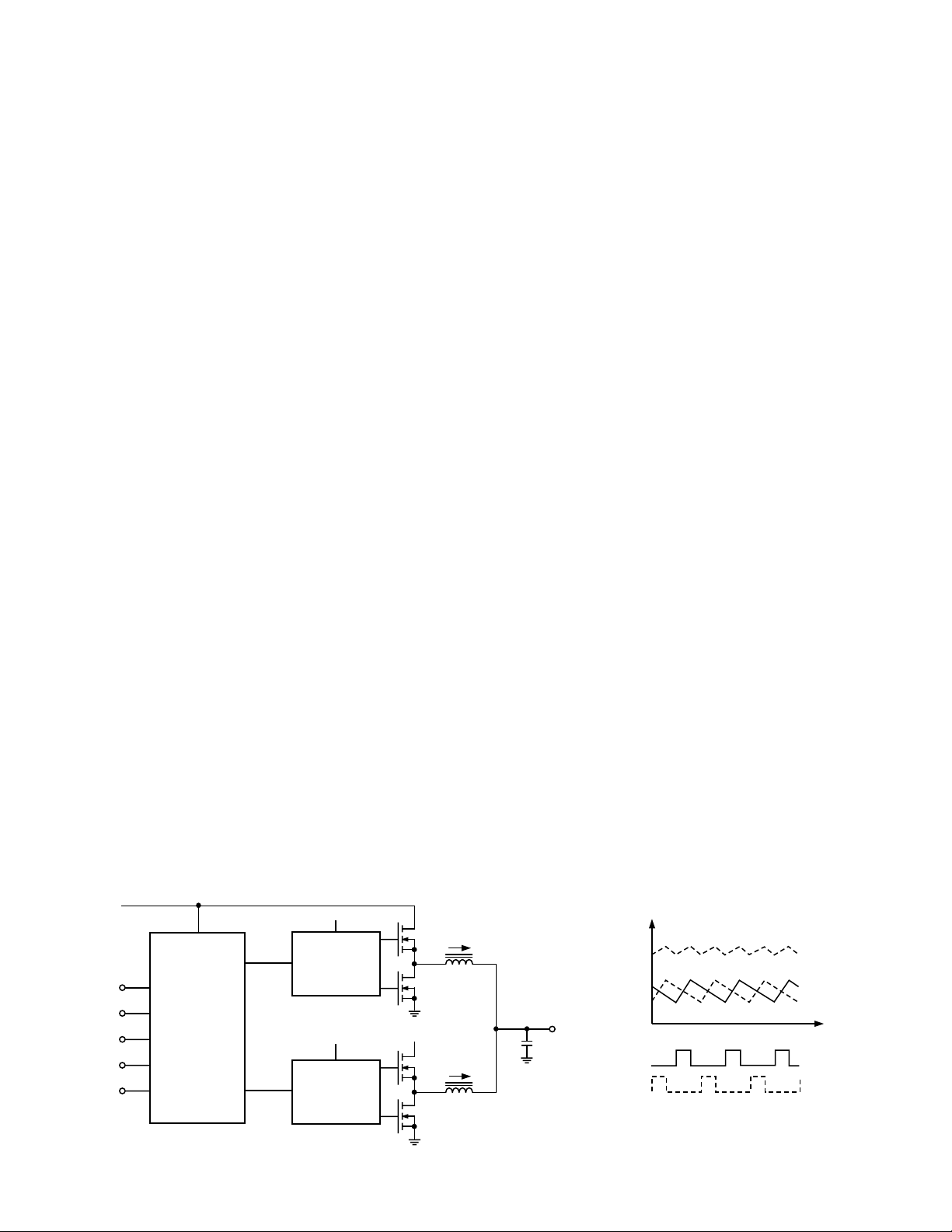
A
system level block diagram of a 2-phase power supply for high
current CPUs is shown in Figure 5.
The frequency of the device is set by an external capacitor
connected to the CT pin. Each output phase operates at half of
the frequency set by the CT pin. The error amplifier and
current sense comparator control the duty cycle of the PWM
outputs to maintain regulation. The maximum duty cycle per
phase is inherently limited to 50% because the PWM outputs
toggle in 2-phase operation. While one phase is on, the other
phase is off. In no case can both outputs be high at the same time.
Output Voltage Sensing
The output voltage is sensed at the FB pin allowing for remote
sensing. To maintain the accuracy of the remote sensing, the
GND pin should also be connected close to the load. A voltage
error amplifier (g
) amplifies the difference between the output
m
voltage and a programmable reference voltage. The reference voltage is programmed between 1.1 V and 1.85 V by an internal 5-bit
DAC that reads the code at the voltage identification (VID) pins.
Refer to Table I for the output voltage versus VID pin code
information.
Active Voltage Positioning
The ADP3160 and ADP3167 use Analog Devices Optimal
Positioning Technology (ADOPT), a unique supplemental
regulation technique that uses active voltage positioning and
provides optimal compensation for load transients. When implemented, ADOPT adjusts the output voltage as a function of the
load current, so that it is always optimally positioned for a load
transient. Standard (passive) voltage positioning has poor dynamic
performance, rendering it ineffective under the stringent repetitive
transient conditions required by high-performance processors.
ADOPT, however, provides optimal bandwidth for transient
response that yields optimal load transient response with the
minimum number of output capacitors.
Reference Output
A 3.0 V reference is available and is commonly used to set the
voltage positioning accurately using a resistor divider to the
COMP pin. In addition, the reference can be used for other
functions such as generating a regulated voltage with an external
amplifier. The reference is bypassed with a 1 nF capacitor to
ground. It is not intended to supply current to large capacitive
loads, and it should not be used to provide more than 1 mA of
output current.
Cycle-by-Cycle Operation
During normal operation (when the output voltage is regulated), the
voltage-error amplifier and the current comparator are the main
control elements. The voltage at the CT pin of the oscillator ramps
between 0 V and 3 V. When that voltage reaches 3 V, the oscillator
sets the driver logic, which sets PWM1 high. During the ON time
of Phase 1, the driver IC turns on the high-side MOSFET. The CS+
and CS– pins monitor the current through the sense resistor that
feeds both high-side MOSFETs. When the voltage between the
two pins exceeds the threshold level set by the voltage error ampli-
), the driver logic is reset and the PWM output goes low.
fier (g
m
This signals the driver IC to turn off the high-side MOSFET and
turn on the low-side MOSFET. On the next cycle of the oscillator,
the driver logic toggles and sets PWM2 high. On each following
cycle of the oscillator, the outputs toggle between PWM1 and
PWM2. In each case, the current comparator resets the PWM
output low when the current comparator threshold is reached. As
the load current increases, the output voltage starts to decrease.
This causes an increase in the output of the g
amplifier, which in
m
turn leads to an increase in the current comparator threshold,
thus programming more current to be delivered to the output so
that voltage regulation is maintained.
5V
OR
12V
VID INPUTS
ADP3160/
ADP3167
2-PHASE
SYNCHRONOUS
BUCK
CONTROLLER
5V
I
PWM1
PWM2
ADP3412
SYNCHRONOUS
DRIVER
5V
ADP3412
SYNCHRONOUS
DRIVER
5V OR 12V
L1
OUT
+
I
L2
I
PWM2
PWM1
OUT
I
L2
Figure 5. 2-Phase CPU Supply System Level Block Diagram
I
L1
REV. B–6–

ADP3160/ADP3167
Active Current Sharing
The ADP3160 and ADP3167 ensure current balance in the two
phases by actively sensing the current through a single sense resistor.
During one phase’s ON time, the current through the respective
high-side MOSFET and inductor is measured through
resistor (R4 in Figure 6). When the comparator (CMP1
Functional Block Diagram) threshold programmed by the g
the sense
in the
ampli-
m
fier is reached, the high-side MOSFET turns off. In the next cycle,
the device switches to the second phase. The current is
measured
with the same sense resistor and the same internal comparator,
ensuring accurate matching. This scheme is immune to imbalances
in the MOSFETs’ R
and inductors’ parasitic resistances.
DS(ON)
If for some reason one of the phases fails, the other phase will
still be limited to its maximum output current (one-half of the
short circuit current limit). If this is not sufficient to supply the
load, the output voltage will droop and cause the PWRGD
output to signal that the output voltage has fallen out of its
specified range.
Short Circuit Protection
The ADP3160 and ADP3167 have multiple levels of short
circuit protection to ensure fail-safe operation. The sense resistor and the maximum current sense threshold voltage given in
the specifications set the peak current limit.
When the load current exceeds the current limit, the excess current
discharges the output capacitor. When the output voltage is
below the foldback threshold V
output current is cut by reducing the current sense threshold
from the current limit threshold, V
old, V
oscillator frequency is reduced by a factor of 5 when the output is
0 V. This further reduces the average current in short circuit.
Power Good Monitoring
The Power Good comparator monitors the output voltage of the
supply via the FB pin. The PWRGD pin is an open-drain output
whose high level (when connected to a pull-up resistor) indicates
that the output voltage is within the specified range of the nominal output voltage requested by the VID DAC. PWRGD will go
low if the output is outside this range.
Output Crowbar
The ADP3160 and ADP3167 include a crowbar comparator that
senses when the output voltage rises higher than the specified trip
threshold, V
and sets both PWM outputs low. The driver ICs turn off the
high-side MOSFETs and turn on the low-side MOSFETs, thus
pulling the output down as the reversed current builds up in the
inductors. If the output overvoltage is due to a short of the highside MOSFET, this action will current limit the input supply or
Table I. Output Voltage vs. VID Code
VID4 VID3 VID2 VID1 VID0 V
OUT(NOM)
11111No CPU
111101.100 V
111011.125 V
111001.150 V
110111.175 V
110101.200 V
110011.225 V
110001.250 V
101111.275 V
101101.300 V
101011.325 V
101001.350 V
100111.375 V
100101.400 V
100011.425 V
100001.450 V
011111.475 V
blow its fuse, protecting the microprocessor from destruction.
The crowbar comparator releases when the output drops below the
specified reset threshold, and the controller returns to normal
operation if the cause of the overvoltage failure does not persist.
Output Disable
The ADP3160 and ADP3167 include an output disable function
that turns off the control loop to bring the output voltage to 0 V.
Because an extra pin is not available, the disable feature is accomplished by pulling the COMP pin to ground. When the COMP pin
drops below 0.56 V for the ADP3160 and 0.64 V for the ADP3167,
the oscillator stops and both PWM signals are driven low. This
function does not place the part in a low quiescent current shutdown state, and the reference voltage is still available. The COMP
pin should be pulled down with an open collector or open-drain
type of output capable of sinking at least 2 mA.
APPLICATION INFORMATION
A VRM 9.0-Compliant Design Example
The design parameters for a typical high-performance Intel CPU
application (see Figure 6) are as follows:
011101.500 V
011011.525 V
011001.550 V
010111.575 V
010101.600 V
010011.625 V
010001.650 V
001111.675 V
001101.700 V
001011.725 V
001001.750 V
000111.775 V
000101.800 V
000011.825 V
000001.850 V
, the maximum deliverable
FB(LOW)
, to the foldback thresh-
CS(FOLD)
Input Voltage (V
. Along with the resulting current foldback, the
CROWBAR
. This comparator overrides the control loop
) = 12 V
IN
Nominal Output Voltage (V
Static Output Tolerance (V
CS(CL)
) = 1.7 V
OUT
) = (V+) – (V–) =
⌬
0 mV – (–130 mV) = 130 mV
Average Output Tolerance (V =
OUT
+
(V+) + (V–)
2
= . V
1 635
V
AVG
)
Maximum Output Current (IO) = 53.4 A
Output Current di/di < 50 A/s
REV. B
–7–

ADP3160/ADP3167
270F ⴛ 4
1
2
3
4
5
6
7
8
C1
150pF
C12
ADP3160
VID4
VID3
VID2
VID1
VID0
COMP
FB
CT
OS-CON 16V
U1
PWM1
PWM2
PWRGD
V
IN
12V
V
RTN
IN
R
A
26.1k⍀
C
OC
3.3nF
R
B
11.0k⍀
C2
100pF
NC = NO CONNECT
FROM
CPU
C11
R1
1k⍀
R7
20⍀
R4
4m⍀
1F
U2
DRVH
SW
PGND
DRVL
RUBYCON MBZ 6.3V
C15 C16
C9
VCC
REF
CS–
CS+
GND
C13
C26
R6
1F
C6
C23
15nF
D2
MBR052LTI
4.7F
Z1
ZMM5236BCT
ADP3414
BST
1
IN
2
NC
3
4
VCC
U3
R5
2.4k⍀
DRVH
SW
PGND
DRVL
C10
1F
8
7
6
5
Q5
2N3904
C14
10⍀
C4
4.7F
16
C25 1nF
15
14
13
12
11
10
9
1F
C5
D1
MBR052LTI
Q3
FDB7030L
Q4
FDB8030L
1
2
3
4
600nH
BST
IN
NC
VCC
ADP3414
L2
Figure 6. 53.4 A Intel CPU Supply Circuit, VRM 9.0 FMB Design
2200F ⴛ 9
C18
C17
Q1
FDB7030L
Q2
FDB8030L
C19
C20 C21
8
7
6
5
13m⍀ ESR (EACH)
L1
600nH
C22
C23
V
CC(CORE)
1.1V – 1.85V
53.4A
V
CC(CORE)
RTN
CT Selection—Choosing the Clock Frequency
The ADP3160 and ADP3167 use a fixed-frequency control architecture. The frequency is set by an external timing capacitor, C
The value of C
for a given clock frequency can be selected using
T
the graph in Figure 2.
The clock frequency determines the switching frequency, which
.
T
For 12.5 A peak-to-peak ripple current, which corresponds to
just under 50% of the 26.7 A full-load dc current in an inductor, Equation 1 yields an inductance of:
relates directly to switching losses and the sizes of the inductors
and input and output capacitors. A clock frequency of 400 kHz
sets the switching frequency of each phase, fSW, to 200 kHz, which
represents a practical trade-off between the switching losses and
the sizes of the output filter components. From Figure 2, for 400 kHz
the required timing capacitor value is 150 pF. For good frequency
stability and initial accuracy, it is recommended to use a capacitor
with a low temperature coefficient and tight tolerance, e.g., an
MLC capacitor with NPO dielectric and with 5% or less tolerance.
Inductance Selection
The choice of inductance determines the ripple current in the
A 600 nH inductor can be used, which gives a calculated ripple
current of 12.2 A at no load. The inductor should not saturate
at the peak current of 32.8 A and should be able to handle the
sum of the power dissipation caused by the average current of
26.7 A in the winding and the core loss.
The output ripple current is smaller than the inductor ripple
current due to the two phases partially canceling. This can be
calculated as follows:
inductor. Less inductance leads to more ripple current, which
increases the output ripple voltage and the conduction losses in
the MOSFETs, but allows using smaller size inductors and, for
a specified peak-to-peak transient deviation, output capacitors
with less total capacitance. Conversely, a higher inductance
means lower ripple current and reduced conduction losses,
but requires larger size inductors and more output capacitance
for the same peak-to-peak transient deviation. In a 2-phase
converter a practical value for the peak-to-peak inductor ripple
current is under 50% of the dc current in the same inductor.
A choice of 46% for this particular design example yields a total
peak-to-peak output ripple current of 23% of the total dc output
current. The following equation shows the relationship between
the inductance, oscillator frequency, peak-to-peak ripple current
in an inductor, and input and output voltages.
Designing an Inductor
Once the inductance is known, the next step is either to design
an inductor or find a standard inductor that comes as close as
possible to meeting the overall design goals. The first decision in
designing the inductor is to choose the core material. There are
several possibilities for providing low core loss at high frequencies. Two examples are the powder cores (e.g., Kool-Mm
Magnetics) and the gapped soft ferrite cores (e.g., 3F3 or 3F4
from Philips). Low-frequency powdered iron cores should be
avoided due to their high core loss, especially when the inductor
value is relatively low and the ripple current is high.
VV V
(– )
IN AVG AVG
L
=
Vf I
¥¥
IN SW L RIPPLE
VV V
(–. ).
12 1 635 1 635
L
V kHz A
¥¥
12 400 2 12 5
¥¥
22
I
=
O
D
¥¥
21635 12 2 1 635
.(–.)
VnHkHz
¥¥
12 600 400
¥
()
¥
/.
VV V
(– )
AVG IN AVG
VLf
¥¥
IN OSC
VV V
=
=
565
=
99
.
(1)
nH=
(2)
A
®
from
REV. B–8–

ADP3160/ADP3167
Two main core types can be used in this application. Open
magnetic loop types, such as beads, beads on leads, and rods and
slugs, provide lower cost but do not have a focused magnetic field
in the core. The radiated EMI from the distributed magnetic
field may create problems with noise interference in the circuitry
surrounding the inductor. Closed-loop types, such as pot cores,
PQ, U, and E cores, or toroids, cost more, but have much
better EMI/RFI performance. A good compromise between
price and performance are cores with a toroidal shape.
There are many useful references for quickly designing a power
inductor. Table II gives some examples.
Table II. Magnetics Design References
Magnetic Designer Software
Intusoft (www.intusoft.com)
Designing Magnetic Components for High-Frequency DC-DC
Converters
McLyman, Kg Magnetics
ISBN 1-883107-00-08
Selecting a Standard Inductor
The companies listed in Table III can provide design consultation and deliver power inductors optimized for high power
applications upon request.
Table III. Power Inductor Manufacturers
Coilcraft
(847) 639-6400
www.coilcraft.com
Coiltronics
(561) 752-5000
www.coiltronics.com
Sumida Electric Company
(510) 668-0660
www.sumida.com
C
Selection—Determining the ESR
OUT
The required equivalent series resistance (ESR) and capacitance
drive the selection of the type and quantity of the output capacitors.
The ESR must be small enough to contain the voltage deviation caused by a maximum allowable CPU transient current
within the specified voltage limits, giving consideration also to the
output ripple and the regulation tolerance. The capacitance must
be large enough that the voltage across the capacitor, which is the
sum of the resistive and capacitive voltage deviations, does not
deviate beyond the initial resistive deviation while the inductor
current ramps up or down to the value corresponding to the new
load current. The maximum allowed ESR also represents the
maximum allowed output resistance, R
OUT
.
The cumulative errors in the output voltage regulations cut into
the available regulation window, V
. When considering dynamic
WIN
load regulation this relates directly to the ESR. When considering dc load regulation, this relates directly to the programmed
output resistance of the power converter.
Some error sources, such as initial voltage accuracy and ripple
voltage, can be directly deducted from the available regulation
window. Other error sources scale proportionally to the
amount of voltage positioning used, which, for an optimal design,
should use the maximum that the regulation window will allow.
The error determination is a closed-loop calculation, but it can
be closely approximated. To maintain a conservative design while
avoiding an impractical design, various error sources should
be considered and summed statistically.
The output ripple voltage can be factored into the calculation by
summing the output ripple current with the maximum output
current to determine an effective maximum dynamic current
change. The remaining errors are summed separately according
to the formula:
VVV k
Ê
Á
Á
Ë
where k
I
O
–
1
II
+
OO
D
= 0.7% is the initial programmed voltage tolerance
VID
from the graph of Figure 4, k
current sense resistor, k
current sense filter components, k
two termination resistors added at the COMP pin, and k
accounts for the IC current loop gain tolerance including the g
(–( ))
=¥¥
WIN VID VID
D
Ê
k
2
k
RCS
CSF
+
Á
2
Ë
RCS
= 20% is the summed tolerance of the
CSF
2
2
ˆ
˜
¯
22
kk mV
++
RT EA
= 2% is the tolerance of the
= 2% is the tolerance of the
RT
ˆ
˜
=
˜
¯
94
EA
(3)
= 8%
m
tolerance.
The remaining window is then divided by the maximum output
current plus the ripple to determine the maximum allowed ESR
and output resistance:
V
RR
E MAX OUT MAX
R
E MAX
==
() ()
mV
94
=
()
AA
53 4 9 9
..
+
WIN
II
+
OO
D
15
.
=
(4)
m
W
The output filter capacitor bank must have an ESR of less than
1.5 mW. One can, for example, use nine MBZ-type capacitors
from Rubycon, with 2.2 mF capacitance, a 6.3 V voltage rating,
and 13 mW ESR. The nine capacitors have a maximum total ESR
of 1.44 mW when connected in parallel. Without ADOPT voltage
positioning, the ESR would need to be less than 0.9 mW, yielding
a 50% increase to 14 MBZ-type output capacitors.
C
—Checking the Capacitance
OUT
As long as the capacitance of the output capacitor is above a
critical value and the regulating loop is compensated with
ADOPT, the actual value has no influence on the peak-to-peak
deviation of the output voltage to a full step change in the load
current. The critical capacitance can be calculated as follows:
C
OUT CRIT
C
OUT CRIT
=
()
=
()
I
O
¥
RV
E OUT
53 4
..
144 17
m
.
W¥
L
¥
2
A
600
nH
¥=
2
.
65
(5)
mF
The critical capacitance for the nine Rubycon capacitors with
an equivalent ESR of 1.44 mW is 6.5 mF, while the equivalent
capacitance of those nine capacitors is 9 ¥ 2.2 mF = 19.8 mF.
Therefore, the capacitance is safely above the critical value.
REV. B
–9–

ADP3160/ADP3167
R
SENSE
The value of R
is based on the maximum required output
SENSE
current. The current comparator of the ADP3160 has a minimum current limit threshold of 142 mV. Note that the 142 mV
value cannot be used for the maximum specified nominal current,
as headroom is needed for ripple current and tolerances.
The current comparator threshold sets the peak of the inductor
current yielding a maximum output current, IO, which equals
twice the peak inductor current value less half of the peak-topeak inductor ripple current. From this the maximum value of
is calculated as:
R
SENSE
R
SENSE
V
CS CL MIN
()( )
£
I
I
LRIPPLE
()
O
+
22
=
mV
142
AA
+
..
26 7 6 1
m
=W
.
43
(6)
In this case, 4 mW was chosen as the closest standard value.
Once R
where current limit is reached, I
has been chosen, the output current at the point
SENSE
, can be calculated using
OUT(CL)
the maximum current sense threshold of 172 mV:
V
CS CL MAX
I
OUT CL
172
¥
2
=¥ =
mV
W
4
m
()( )
2
R
SENSE
–. .
12 2 73 8
=
AA
–
I
L RIPPLE()
()
(7)
At output voltages below 425 mV, the current sense threshold is
reduced to 95 mV, and the ripple current is negligible. Therefore, at dead short the output current is reduced to:
I
OUT SC()
95
.=¥ =2
A
47 5
m
4
W
(8)
mV
To safely carry the current under maximum load conditions, the
sense resistor must have a power rating of at least:
PI R
=¥
R SENSE RMS SENSE
SENSE
2
()
(9)
where:
2
I
I
SENSE RMS
2
()
=¥
V
O OUT
n
V
¥h
IN
(10)
In this formula, n is the number of phases, and is the converter
efficiency, in this case assumed to be 85%. Combining Equations 9
and 10 yields:
2
..
AV
P
R
53 4
=¥¥¥W=
SENSE
2
17
.
085 12
mmW
4 950
V
Power MOSFETs
In the standard 2-phase application, two pairs of N-channel
power MOSFETs must be used with the ADP3160 and
ADP3412, one pair as the main (control) switches and the
other pair as the synchronous rectifier switches. The main
selection parameters for the power MOSFETs are V
and R
. The minimum gate drive voltage (the supply volt-
DS(ON)
GS(TH)
age to the ADP3412) dictates whether standard threshold or
logic-level threshold MOSFETs must be used. Since V
logic-level threshold MOSFETs (V
< 2.5 V) are strongly
GS(TH)
GATE
< 8 V,
recommended.
The maximum output current I
determines the R
O
DS(ON)
requirement for the power MOSFETs. When the ADP3160 is operating
in continuous mode, the simplifying assumption can be made
that in each phase one of the two MOSFETs is always conducting the average inductor current. For V
V
= 1.6 V, the duty ratio of the high-side MOSFET is:
OUT
V
D
OUT
==13 3.%
HSF
V
IN
= 12 V and
IN
(11)
The duty ratio of the low-side (synchronous rectifier) MOSFET is:
DD
==1867–.%
LSF HSF
(12)
The maximum rms current of the high-side MOSFET during
normal operation is:
I
HSF MAX
()
Ê
I
O
D
HSF
2
I
()
LRIPPLE
1
Á
Ë
¥
3
ˆ
=
98
˜
2
I
¯
O
(13)
A
.=¥+
2
The maximum rms current of the low-side MOSFET during
normal operation is:
II
LSF MAX HSF MAX
==25
() ()
The R
for each MOSFET can be derived from the allowable
DS(ON)
LSF
D
HSF
A
(14)
D
dissipation. If 10% of the maximum output power is allowed for
MOSFET dissipation, the total dissipation in the four MOSFETs
of the 2-phase converter will be:
PVI
MOSFET TOTAL MIN O
PVAW
MOSFET TOTAL
()
()
.
=¥ ¥
01
.. . .
=¥ ¥ =
01 157 534 84
(15)
Allocating half of the total dissipation for the pair of high-side
MOSFETs and half for the pair of low-side MOSFETs, and
assuming that the resistive and switching losses of the high-side
MOSFET are equal, the required maximum MOSFET resistances will be:
R
()( )
DS ON HS MAX
R
()( )
DS ON HS MAX
R
()( )
DS ON LS MAX
R
()( )
DS ON LS MAX
P
MOSFET TOTAL
=
8
=
898
P
MOSFET TOTAL
=
4
=
425
()
2
¥
I
HSF MAX
.
84
W
(. )
¥
A
()
2
¥
I
LSF MAX
.
84
W
()
¥
A
()
=W
11
m
2
()
.
=W
34
2
m
(16)
(17)
Note that there is a trade-off between converter efficiency and
cost. Larger MOSFETs reduce the conduction losses and allow
higher efficiency, but increase the system cost. If efficiency is
not a major concern, a Fairchild FDB7030L (R
DS(ON)
= 7 mW
nominal, 10 mW worst case) for the high-side and a Fairchild
FDB8030L (R
= 3.1 mW nominal, 5.6 mW worst case)
DS(ON)
for the low-side are good choices. The high-side MOSFET
dissipation is:
PR I
=¥
()
HSF DS ON HS
VI Qf
¥¥¥
IN L PK G
()
()
I
¥
2
G
2
HFS MAX
()
SW
VQ f
+¥¥
()
+
(18)
IN RR SW
where the second term represents the turn-off loss of the
MOSFET and the third term represents the turn-on loss due to
the stored charge in the body diode of the low-side MOSFET.
(In the second term, Q
the gate for turn-off and I
is the gate charge to be removed from
G
is the gate turn-off current. From
G
REV. B–10–

ADP3160/ADP3167
the data sheet for the FDB7030L, the value of QG is about 35 nC
and the peak gate drive current provided by the ADP3412 is
about 1 A. In the third term, Q
is the charge stored in the
RR
body diode of the low-side MOSFET at the valley of the inductor
current. The data sheet of the FDB8030L does not give that
information, so an estimated value of 150 nC is used. The estimate is based on information found on the data sheet of a
similar device, the IRF7809. In both terms, f
switching frequency of the MOSFETs, or 200 kHz. I
is the actual
SW
L(PK)
is the
peak current in the inductor, or 32.8 A.
Substituting the above data in Equation 19, and using the worstcase value for the MOSFET resistance yields a conduction loss
of 0.96 W, a turn-off loss of 2.75 W, and a turn-on loss of 0.72 W.
Thus the worst-case total loss in a high-side MOSFET is 4.43 W.
The worst-case low-side MOSFET dissipation is:
PR I
=¥
LSF DS ON LS
PmAW
LSF
()
.().
56 25 35
=W¥ =
2
LSF MAX
()
2
(19)
(Note that there are no switching losses in the low-side MOSFET.)
CIN Selection and Input Current di/dt Reduction
In continuous inductor-current mode, the source current of the
high-side MOSFET is approximately a square wave with a duty
ratio equal to V
OUT/VIN
and an amplitude of one-half of the
maximum output current. To prevent large voltage transients, a
low ESR input capacitor sized for the maximum rms current
must be used. The maximum rms capacitor current is given by:
I
C RMS
()
I
C RMS
()
I
O
=¥-¥
53 4
=¥¥=
DD
22
2
A
.
2
()
HSF HSF
.–( .) .
20133 20133 11 9
2
(20)
2
A
Note that the capacitor manufacturer’s ripple current ratings are
often based on only 2000 hours of life. This makes it advisable
to further derate the capacitor, or to choose a capacitor rated at
a higher temperature than required. Several capacitors may be
placed in parallel to meet size or height requirements in the
design. In this example, the input capacitor bank is formed by
four 270 mF, 16 V OS-CON capacitors.
The ripple voltage across the three paralleled capacitors is:
V
C RIPPLE
()
V
C RIPPLE
()
Ê
InESR
OCCHSF
=¥ +
Á
nDnC f
Ë
Am
.
53 4218
=¥W+
CINSW
Ê
Á
4
Ë
¥¥
4 270 200
ˆ
˜
¯
0 133
.
F kHz
¥m¥
(21)
ˆ
mV
=
137
˜
¯
To reduce the input current di/dt to below the recommended
maximum of 0.1 A/ms, an additional small inductor (L > 1 mH@
15 A) should be inserted between the converter and the supply
bus. That inductor also acts as a filter between the converter and
the primary power source.
Feedback Loop Compensation Design for ADOPT
Optimized compensation of the ADP3160 and ADP3167 allow
the best possible containment of the peak-to-peak output voltage
deviation. Any practical switching power converter is inherently
limited by the inductor in its output current slew rate to a value
much less than the slew rate of the load. Therefore, any sudden
change of load current will initially flow through the output capacitors, and assuming that the capacitance of the output capacitor
is larger than the critical value defined by Equation 5, this will
produce a peak output voltage deviation equal to the ESR of the
output capacitor times the load current change.
The optimal implementation of voltage positioning, ADOPT,
will create an output impedance of the power converter that is
entirely resistive over the widest possible frequency range, including dc, and equal to the maximum acceptable ESR of the output
capacitor array. With the resistive output impedance, the output
voltage will droop in proportion with the load current at any
load current slew rate; this ensures the optimal positioning and
allows the minimization of the output capacitor.
With an ideal current-mode controlled converter, where the
average inductor current would respond without delay to the
command signal, the resistive output impedance could be
achieved by having a single-pole roll-off of the voltage gain of
the voltage-error amplifier. The pole frequency must coincide
with the ESR zero of the output capacitor. The devices use constant
frequency current-mode control, which is known to have a
nonideal, frequency dependent command signal to inductor current
transfer function. The frequency dependence manifests in the
form of a pair of complex conjugate poles at one-half of the switching frequency. A purely resistive output impedance could be
achieved by canceling the complex conjugate poles with zeros at
the same complex frequencies and adding a third pole equal to
the ESR zero of the output capacitor. Such a compensating network
would be quite complicated. Fortunately, in practice it is
sufficient to cancel the pair of complex conjugate poles with a
single real zero placed at one-half of the switching frequency.
Although the end result is not a perfectly resistive output impedance, the remaining frequency dependence causes only a small
percentage of deviation from the ideal resistive response. The
single-pole and single-zero compensation can be easily implemented
by terminating the g
error amplifier with the parallel combina-
m
tion of a resistor and a series RC network.
The first step in the design of the feedback loop compensation is to determine the targeted output resistance, R
E(MAX)
, of the
power converter using Equation 4. The compensation can then
be tailored to create that output impedance for the power
converter, and the quantity of output capacitors can be chosen
to create a net ESR that is less than or equal to R
E(MAX)
.
The next step is to determine the total termination resistance of
the g
amplifier that will yield the correct output resistance:
m
nR
¥
R
T
R
T
I SENSE
=
gR
¥¥
mEMAX
()
.
12 5 4
=
..
22 15 2
mmho m
2
m
¥W
¥W¥
.
757
k
=W
(22)
where nI is the division ratio from the output voltage signal of
the g
amplifier to the PWM comparator (CMP1), gm is the
m
transconductance of the g
amplifier itself, and the factor of 2 is
m
the result of the 2-phase configuration. Note that the internal
current multiplier (n
) is 12.5 for the ADP3160, but is 25 for
I
the ADP3167. For this example, assume that we use the
Rubycon capacitors at the output with their ESR of 1.44 mW.
Once R
from the REF pin to output of the g
is known, the two resistors that make up the divider
T
amplifier (COMP pin)
m
must be calculated. The resistive divider introduces an offset to
the output of the g
the gain of the g
amplifier that, when reflected back through
m
stage, accurately positions the output voltage
m
near its allowed maximum at light load. Furthermore, the output
of the g
amplifier sets the current sense threshold voltage. At no
m
load, the current sense threshold is increased by the peak of the
ripple current in the inductor and reduced by the delay between
REV. B
–11–

ADP3160/ADP3167
sensing when the current threshold has been reached and when
the high-side MOSFET actually turns off. These two factors are
combined with the inherent voltage at the output of g
that commands a current sense threshold of 0 mV (V
IRn
L RIPPLE SENSE I
VV
=+
GNL GNL
VV
-
IN AVG
L
VV+
=
1
GNL
V– . V
12 1 635
nH
600
()
0
¥¥¥ ¥
2
tR n
()
D SENSE I
.A m .
12 2 4 12 5
¥¥ ¥ ¥
260 4 1251201
The output voltage at no load (V
¥¥
2
¥¥
W
2
ns m . = . V
–
W
) can be calculated by
ONL
-
amplifier
m
):
GNL0
(23)
starting with the VID setting, adding in the positive offset (V+),
subtracting half the ripple voltage, and then subtracting the
dominant error terms:
RI
VVV
=+- -¥
ONL VID
2
kk
+¥
VID RT
VVV
17 0007 002
17 0
=+-
ONL
.(.).
.
V
¥+¥
+
Ê
V
Á
Ë
WIN
V
2
With these two terms calculated, the divider resistors (R
D
EO
V
2
ˆ
˜
¯
VID
138 99
..
VID
2
mA
W¥
2
Ê
Á
Ë
94
17
.
mV
V
(24)
–
2
ˆ
1 681
=
˜
¯
V
.
A
for the upper and RB for the lower) can be calculated.
Assuming that the internal resistance of the g
(R
) is 200 kW:
OGM
amplifier
m
Choosing the nearest 1% resistor value gives RB = 11.0 kW.
Finally, R
is calculated:
A
R
=
A
111
--
RR R
T OGM B
=
R
A
1
757
..
kk k
1
(26)
1
1
-
200
W
W
-
1
11 3
25 86
.
=W
k
W
Again, choosing the nearest 1% resistor value gives RA= 26.1 kW.
The compensating capacitor can be calculated from the equation:
CR
¥
C
C
p
OUT E MAX
=
OC
19 8 1 5
..
=
OC
kHz k
¥¥W
400 7 57
()
RfR
T OSC T
mF m
757
.
2
-
¥W
k
W
.
=
2
¥¥
p
-
nF
35
.
(27)
The closest standard value for COC is 3.3 nF.
The resistance of the zero-setting resistor in series with the
compensating capacitor is:
R
=
Z
R
=
Z
2
Cf
¥¥
p
OC OSC
2
nF kHz
¥¥
33 400
p.
=W
482
(28)
The nearest standard 5% resistor value is 470 W. Note that this
resistor is only required when C
25% or less). In this example, C
OUT
OUT
approaches C
> C
, and RZ can there-
CRIT
CRIT
(within
fore be omitted.
R
=
B
VV
R
=
B
–
REF GNL
R
T
VV
-
312
.
-¥
k
W
757
.
V
REF
-¥ -
()
gV V
m ONL VID
V
3
mmho V V
22 1681 17
.(.–.)
10 73
.
k
=W
(25)
REV. B–12–

1
2
Ch1
500mV 20mV 700mVCh1M 200sCh2
Figure 7. Transient Response of the 53.4 A
Design Example of Figure 6
AMD Athlon Design Example
The design parameters for a typical high-performance AMD
CPU application (see Figure 8) are as follows:
Input Voltage (V
Nominal Output Voltage (V
Static Output Tolerance (V
) = 5 V
IN
) = 1.7 V
OUT
) = (V+) – (V–) =
⌬
50 mV – (–50 mV) = 100 mV
Average Output Voltage (V ) =
(V+) + (V–)
+
V
OUT
2
AVG
= 1.7 V
Maximum Output Current (IO) = 45 A
Output Current di/dt < 50 A/s
Using the design procedure previously shown, the final values
for this application were calculated, and are shown in Figure 8.
ADP3160/ADP3167
LAYOUT AND COMPONENT PLACEMENT GUIDELINES
The following guidelines are recommended for optimal performance of a switching regulator in a PC system.
General Recommendations
1. For good results, at least a four-layer PCB is recommended.
This should allow the needed versatility for control circuitry
interconnections with optimal placement, a signal ground
plane, power planes for both power ground and the input
power (e.g., 5 V), and wide interconnection traces in the
rest of the power delivery current paths. Keep in mind that
each square unit of 1 ounce copper trace has a resistance of
~0.53 mW at room temperature.
2. Whenever high currents must be routed between PCB layers,
vias should be used liberally to create several parallel current
paths so that the resistance and inductance introduced by
these current paths is minimized and the via current rating is
not exceeded.
3. If critical signal lines (including the voltage and current
sense lines of the ADP3160) must cross through power
circuitry, it is best if a signal ground plane can be interposed
between those signal lines and the traces of the power
circuitry. This serves as a shield to minimize noise injection into the signals at the expense of making signal ground
a bit noisier.
4. The power ground plane should not extend under signal
components, including the ADP3160 itself. If necessary,
follow the preceding guideline to use the signal ground
plane as a shield between the power ground plane and the
signal circuitry.
5. The GND pin of the ADP3160 should be connected first to
the timing capacitor (on the CT pin), and then into the
signal ground plane. In cases where no signal ground plane
can be used, short interconnections to other signal ground
circuitry in the power converter should be used.
12V V
12V V
R2
20.6k⍀
C
OC
1.8nF
100pF
REV. B
V
IN
CC
V
IN
5V
RTN
CC
RTN
FROM
R3
16.5k⍀
C2
CPU
R1
1k⍀
1800F ⴛ 4
RUBYCON MBZ SERIES
C14C13C12
U1
ADP3167
1
2
3
4
5
6
7
8
C1
150pF
VID4
VID3
VID2
VID1
VID0
COMP
FB
CT
VCC
REF
CS–
PWM1
PWM2
CS+
PWRGD
GND
Z1
U3
R5
2.4k⍀
DRVH
SW
PGND
DRVL
R7
20⍀
C10
1F
8
7
6
5
Q5
2N3904
C5
1F
D1
MBR052LTI
C7
15pF
Q3
FDB7030L
600nH
Q4
FDB7035L
R4
4m⍀
U2
ADP3412
BST
1
DRVH
IN
2
3
4
L2
SW
DLY
PGND
DRVL
VCC
RUBYCON 6.3V MBZ SERIES
13m
C11 C16
C17
C9
1F
8
7
6
5
2200F ⴛ 10
ESR (EACH)
C19
C18
Q1
FDB7030L
Q2
FDB7035L
C20
C24
C25
L1
600nH
C27
C28
V
CC(CORE)
1.1V – 1.85V
45A
V
CC(CORE)
RTN
C15
C26
C21
4.7F
15nF
R6
10⍀
C4
4.7F
16
C22 1nF
15
14
13
12
1F
C6
MBR052LTI
15pF
11
10
9
D2
C8
ZMM5236BCT
ADP3412
BST
1
IN
2
DLY
3
4
VCC
Figure 8. 45 A Athlon Duron CPU Supply Circuit
–13–

ADP3160/ADP3167
6. The output capacitors of the power converter should be
connected to the signal ground plane even though power
current flows in the ground of these capacitors. For this
reason, it is advisable to avoid critical ground connections
(e.g., the signal circuitry of the power converter) in the
signal ground plane between the input and output capacitors.
It is also advisable to keep the planar interconnection path
short (i.e., have input and output capacitors close together).
7. The output capacitors should also be connected as closely
as possible to the load (or connector) that receives the power
(e.g., a microprocessor core). If the load is distributed, the
capacitors should also be distributed, and generally in
proportion to where the load tends to be more dynamic.
8. Absolutely avoid crossing any signal lines over the switching
power path loop, described next.
Power Circuitry
9. The switching power path should be routed on the PCB to
encompass the smallest possible area to minimize radiated
switching noise energy (i.e., EMI). Failure to take proper
precautions often results in EMI problems for the entire PC
system as well as noise-related operational problems in the
power converter control circuitry. The switching power path
is the loop formed by the current path through the input
capacitors, the power MOSFETs, and the power Schottky
diode, if used (see next), including all interconnecting PCB
traces and planes. The use of short and wide interconnection traces is especially critical in this path for two reasons:
it minimizes the inductance in the switching loop, which can
cause high-energy ringing, and it accommodates the high
current demand with minimal voltage loss.
10. An optional power Schottky diode (3 A–5 A dc rating) from
each lower MOSFET’s source (anode) to drain (cathode) will
help to minimize switching power dissipation in the upper
MOSFETs. In the absence of an effective Schottky diode, this
dissipation occurs through the following sequence of switching
events. The lower MOSFET turns off in advance of the upper
MOSFET turning on (necessary to prevent cross-conduction).
The circulating current in the power converter, no longer
finding a path for current through the channel of the lower
MOSFET, draws current through the inherent body diode of
the MOSFET. The upper MOSFET turns on, and the reverse
recovery characteristic of the lower MOSFET’s body diode
prevents the drain voltage from being pulled high quickly. The
upper MOSFET then conducts very large current while it
momentarily has a high voltage forced across it, which translates
into added power dissipation in the upper MOSFET. The
Schottky diode minimizes this problem by carrying a majority of
the circulating current when the lower MOSFET is turned off,
and by virtue of its essentially nonexistent reverse recovery
time. The Schottky diode has to be connected with very short
copper traces to the MOSFET to be effective.
11. A small ferrite bead inductor placed in series with the drain
of the lower MOSFET can also help to reduce this previously
described source of switching power loss.
12. Whenever a power dissipating component (e.g., a power
MOSFET) is soldered to a PCB, the liberal use of vias, both
directly on the mounting pad and immediately surrounding
it, is recommended. Two important reasons for this are:
improved current rating through the vias, and improved
thermal performance from vias extended to the opposite side
of the PCB where a plane can more readily transfer the heat
to the air.
13. The output power path, though not as critical as the switching power path, should also be routed to encompass a small
area. The output power path is formed by the current path
through the inductor, the current sensing resistor, the output capacitors, and back to the input capacitors.
14. For best EMI containment, the power ground plane should
extend fully under all the power components except the
output capacitors. These components are: the input capacitors,
the power MOSFETs and Schottky diodes, the inductors, the
current sense resistor, and any snubbing element that might
be added to dampen ringing. Avoid extending the power
ground under any other circuitry or signal lines, including the
voltage and current sense lines.
Signal Circuitry
15. The output voltage is sensed and regulated between the FB
pin and the GND pin (which connects to the signal ground
plane). The output current is sensed (as a voltage) by the
CS+ and CS– pins. In order to avoid differential mode noise
pickup in the sensed signal, the loop area should be small.
Thus the FB trace should be routed atop the signal ground
plane and the CS+ and CS– pins (the CS+ pin should be
over the signal ground plane as well).
16. The CS+ and CS– traces should be Kelvin-connected to the
current sense resistor, so that the additional voltage drop
due to current flow on the PCB at the current sense resistor
connections does not affect the sensed voltage.
REV. B–14–

OUTLINE DIMENSIONS
Dimensions shown in millimeters and (inches)
16-Lead Standard Small Outline Package [SOIC]
Narrow Body
(R-16A/SO-16)
10.00 (0.3937)
9.80 (0.3858)
4.00 (0.1575)
3.80 (0.1496)
16
1
9
6.20 (0.2441)
5.80 (0.2283)
8
ADP3160/ADP3167
PIN 1
1.27 (0.0500)
COPLANARITY
0.25 (0.0098)
0.10 (0.0039)
CONTROLLING DIMENSIONS ARE IN MILLIMETERS; INCH DIMENSIONS
(IN PARENTHESES) ARE ROUNDED-OFF MILLIMETER EQUIVALENTS FOR
REFERENCE ONLY AND ARE NOT APPROPRIATE FOR USE IN DESIGN
BSC
1.75 (0.0689)
1.35 (0.0531)
0.51 (0.0201)
0.33 (0.0130)
SEATING
PLANE
0.25 (0.0098)
0.19 (0.0075)
0.50 (0.0197)
0.25 (0.0098)
8ⴗ
0ⴗ
1.27 (0.0500)
0.40 (0.0157)
ⴛ 45ⴗ
REV. B
–15–

ADP3160/ADP3167
Revision History
Location Page
05/02—Data Sheet changed from REV. A to REV. B.
Addition of ADP3167 . . . . . . . . . . . . . . . . . . . . . . . . . . . . . . . . . . . . . . . . . . . . . . . . . . . . . . . . . . . . . . . . . . . . . . . . . . . . . .Universal
2/01—Data Sheet changed from REV. 0 to REV. A.
Changes to Reference section of SPECIFICATIONS . . . . . . . . . . . . . . . . . . . . . . . . . . . . . . . . . . . . . . . . . . . . . . . . . . . . . . . . . . . . 2
Edits to Figure 1 . . . . . . . . . . . . . . . . . . . . . . . . . . . . . . . . . . . . . . . . . . . . . . . . . . . . . . . . . . . . . . . . . . . . . . . . . . . . . . . . . . . . . . . . 5
Replacement of Figure 2 . . . . . . . . . . . . . . . . . . . . . . . . . . . . . . . . . . . . . . . . . . . . . . . . . . . . . . . . . . . . . . . . . . . . . . . . . . . . . . . . . . 5
Edits to C
Edits to Figure 6 . . . . . . . . . . . . . . . . . . . . . . . . . . . . . . . . . . . . . . . . . . . . . . . . . . . . . . . . . . . . . . . . . . . . . . . . . . . . . . . . . . . . . . . . 8
Changes to Equations 4, 6, and 24–28 . . . . . . . . . . . . . . . . . . . . . . . . . . . . . . . . . . . . . . . . . . . . . . . . . . . . . . . . . . . . . . . . . 9, 10, 12
Edits to C
Edits to Power MOSFETs Section . . . . . . . . . . . . . . . . . . . . . . . . . . . . . . . . . . . . . . . . . . . . . . . . . . . . . . . . . . . . . . . . . . . . . . . . . 10
Changes to Figure 8 . . . . . . . . . . . . . . . . . . . . . . . . . . . . . . . . . . . . . . . . . . . . . . . . . . . . . . . . . . . . . . . . . . . . . . . . . . . . . . . . . . . . . 13
Selection—Choosing the Clock Frequency section . . . . . . . . . . . . . . . . . . . . . . . . . . . . . . . . . . . . . . . . . . . . . . . . . . . . . 8
T
—Checking the Capacitance section . . . . . . . . . . . . . . . . . . . . . . . . . . . . . . . . . . . . . . . . . . . . . . . . . . . . . . . . . . . . . . 9
OUT
C02806–0–5/02(B)
–16–
PRINTED IN U.S.A.
REV. B

 Loading...