Analog Devices ADP3164 Datasheet

5-Bit Programmable 4-Phase
a
FEATURES
ADOPT™ Optimal Positioning Technology for Superior
Load Transient Response and Fewest Output
Capacitors
Complies with VRM 9.1 with Lowest System Cost
4-Phase Operation at up to 500 kHz per Phase
Quad Logic-Level PWM Outputs for Interface to
External High-Power Drivers
Active Current Balancing between All Output Phases
Accurate Multiple VRM Module Current Sharing
5-Bit Digitally Programmable 1.1 V to 1.85 V Output
Total Output Accuracy ⴞ0.8% Over Temperature
Current-Mode Operation
Short Circuit Protection
Enhanced Power Good Output Detects Open Outputs
in Multi-VRM Power Systems
Overvoltage Protection Crowbar Protects
Microprocessors with No Additional
External Components
APPLICATIONS
Desktop PC Power Supplies for:
Intel Pentium
VRM Modules
®
4 Processors
Synchronous Buck Controller
ADP3164
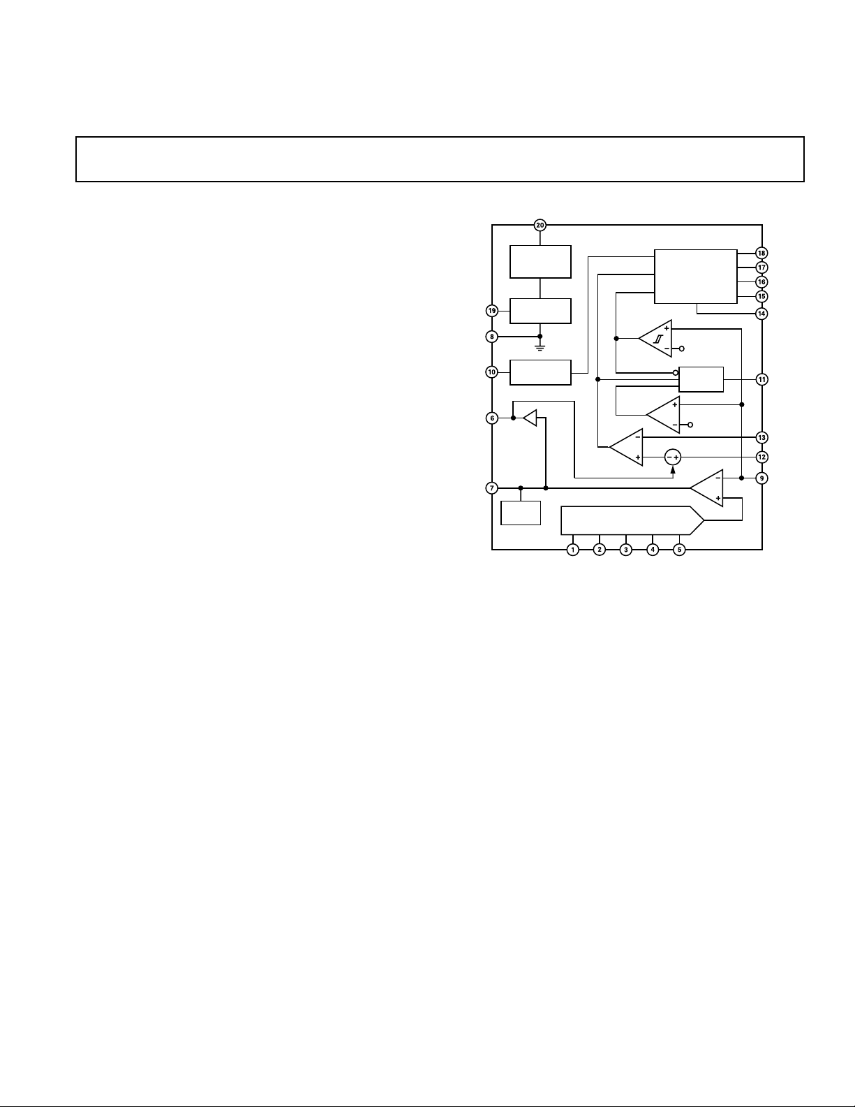
FUNCTIONAL BLOCK DIAGRAM
VCC
REF
GND
CT
SHARE
COMP
UVLO
& BIAS
3.0V
REFERENCE
OSCILLATOR
SOFT
START
ADP3164
VID4
SET
RESET
CROWBAR
CMP
VID
DAC
VID3 VID2 VID1
CMP
4-PHASE
DRIVER
LOGIC
POWER
VID0
DAC + 20%
GOOD
DAC – 20%
g
m
PWM1
PWM2
PWM3
PWM4
PGND
PWRGD
CS–
CS+
FB
GENERAL DESCRIPTION
The ADP3164 is a highly efficient 4-phase synchronous buck
switching regulator controller optimized for converting a 12 V
main supply into the core supply voltage required by high performance Intel processors. The ADP3164 uses an internal 5-bit
DAC to read a voltage identification (VID) code directly from
the processor, which is used to set the output voltage between
1.1 V and 1.85 V. The ADP3164 uses a current mode PWM
architecture to drive the logic-level outputs at a programmable
switching frequency that can be optimized for VRM size and
efficiency. The four output phases share the dc output current
to reduce overall output voltage ripple. An active current balancing function ensures that all phases carry equal portions of
the total load current, even under large transient loads, to minimize the size of the inductors.
ADOPT is a trademark of Analog Devices, Inc.
Pentium is a registered trademark of Intel Corporation.
REV. 0
Information furnished by Analog Devices is believed to be accurate and
reliable. However, no responsibility is assumed by Analog Devices for its
use, nor for any infringements of patents or other rights of third parties that
may result from its use. No license is granted by implication or otherwise
under any patent or patent rights of Analog Devices.
The ADP3164 also uses a unique supplemental regulation technique called active voltage positioning (ADOPT) to enhance
load transient performance. Active voltage positioning results in
a dc/dc converter that meets the stringent output voltage specifications for high-performance processors, with the minimum
number of output capacitors and smallest footprint. Unlike
voltage-mode and standard current-mode architectures, active
voltage positioning adjusts the output voltage as a function of the
load current so that it is always optimally positioned for a system
transient. The ADP3164 also provides accurate and reliable short
circuit protection, adjustable current limiting, and an enhanced
Power Good output that can detect open outputs in any phase for
single or multi-VRM systems.
The ADP3164 is specified over the commercial temperature
range of 0°C to 70°C and is available in a 20-lead TSSOP package.
One Technology Way, P.O. Box 9106, Norwood, MA 02062-9106, U.S.A.
Tel: 781/329-4700 www.analog.com
Fax: 781/326-8703 © Analog Devices, Inc., 2001

1
ADP3164–SPECIFICATIONS
(VCC = 12 V, I
Parameter Symbol Conditions Min Typ Max Unit
FEEDBACK INPUT
Accuracy V
FB
1.1 V Output 1.091 1.1 1.109 V
1.6 V Output 1.587 1.6 1.613 V
1.85 V Output 1.835 1.85 1.865 V
Line Regulation ∆V
Input Bias Current I
FB
Crowbar Trip Point V
FB
CROWBAR
VCC = 10 V to 14 V 0.01 %
% of Nominal Output 115 120 125 %
Crowbar Reset Point % of Nominal Output 40 50 60 %
Crowbar Response Time t
CROWBAR
Overvoltage to PWM Going Low 400 ns
REFERENCE
Output Voltage V
Output Current I
REF
REF
VID INPUTS
Input Low Voltage V
Input High Voltage V
Input Current I
Pull-Up Resistance R
IL(VID)
IH(VID)
VID
VID
VID(X) = 0 V 70 90 µA
Internal Pull-Up Voltage 2.7 3.0 3.3 V
OSCILLATOR
Maximum Frequency
Frequency Variation f
CT Charge Current I
2
f
CT(MAX)
CT
CT
TA = 25°C, CT = 150 pF 475 575 675 kHz
= 25°C, CT = 68 pF 850 1000 1250 kHz
T
A
T
= 25°C, CT = 47 pF 1100 1300 1500 kHz
A
TA = 25°C, VFB in Regulation 260 300 340 µA
TA = 25°C, VFB = 0 V 40 65 80 µA
ERROR AMPLIFIER
Output Resistance R
Transconductance g
Output Current I
Maximum Output Voltage V
Output Disable Threshold V
–3 dB Bandwidth BW
O(ERR)
m(ERR)
O(ERR)
COMP(MAX)
COMP(OFF)
ERR
FB = 0 V 575 µA
FB Forced to V
COMP = Open 500 kHz
CURRENT SENSE
Threshold Voltage V
CS(TH)
CS+ = VCC, 143 158 173 mV
FB Forced to V
FB ≤ 750 mV 80 92 108 mV
0.8 V ≤ SHARE ≤ 1 V 0 5 mV
Input Bias Current I
Response Time t
CS+
CS
, I
CS–
CS+ = CS– = VCC 1 5 µA
CS+ – (CS–) ≥ 173 mV 50 ns
to PWM Going Low
CURRENT SHARING
Output Source Current 2 mA
Output Sink Current 300 400 µA
Maximum Output Voltage V
SHARE(MAX)
FB Forced to V
POWER GOOD COMPARATOR
Undervoltage Threshold V
Overvoltage Threshold V
Output Voltage Low V
PWRGD(UV)
PWRGD(OV)
OL(PWRGD)IPWRGD(SINK)
Percent of Nominal Output 75 80 85 %
Percent of Nominal Output 115 120 125 %
Response Time 250 ns
PWM OUTPUTS
Output Voltage Low V
Output Voltage High V
Duty Cycle Limit Per Phase
2
OL(PWM)
OH(PWM)
DC 25 %
I
PWM(SINK)
I
PWM(SOURCE)
= 150 A, TA = 0ⴗC to 70ⴗC, unless otherwise noted.)
REF
550 nA
2.952 3.00 3.048 V
300 µA
0.8 V
2.0 V
33 43 kΩ
4000 kHz
1MΩ
2.0 2.2 2.45 mmho
– 3% 3.0 V
OUT
800 875 mV
– 3%
OUT
– 3% 3.0 V
OUT
= 1 mA 375 525 mV
= 400 µA 100 500 mV
= 400 µA 4.0 5.0 V
–2–
REV. 0

ADP3164
WARNING!
ESD SENSITIVE DEVICE
Parameter Symbol Conditions Min Typ Max Unit
SUPPLY
DC Supply Current
Normal Mode I
No CPU Mode I
UVLO Mode I
UVLO Threshold Voltage V
CC
CC(NO CPU)
CC(UVLO)
UVLO
VID4 – VID0 = Open 3.5 5.5 mA
VCC ≤ V
, VCC Rising 350 500 µA
UVLO
5.9 6.4 6.9 V
UVLO Hysteresis 0.5 0.8 1.0 V
NOTES
1
All limits at temperature extremes are guaranteed via correlation using standard Statistical Quality Control (SQC).
2
Guaranteed by design, not tested in production.
Specifications subject to change without notice.
3.75 5.5 mA
ABSOLUTE MAXIMUM RATINGS*
VCC . . . . . . . . . . . . . . . . . . . . . . . . . . . . . . . –0.3 V to +15 V
CS+, CS– . . . . . . . . . . . . . . . . . . . . . . –0.3 V to VCC +0.3 V
All Other Inputs and Outputs . . . . . . . . . . . . –0.3 V to +10 V
Operating Ambient Temperature Range . . . . . . . 0°C to 70°C
Operating Junction Temperature . . . . . . . . . . . . . . . . . . 125°C
Storage Temperature Range . . . . . . . . . . . . –65°C to +150°C
. . . . . . . . . . . . . . . . . . . . . . . . . . . . . . . . . . . . . . . 143°C/W
θ
JA
Lead Temperature (Soldering, 10 sec) . . . . . . . . . . . . . 300°C
Vapor Phase (60 sec) . . . . . . . . . . . . . . . . . . . . . . . . . . . 215°C
Infrared (15 sec) . . . . . . . . . . . . . . . . . . . . . . . . . . . . . . 220°C
*This is a stress rating only; operation beyond these limits can cause the device to
be permanently damaged. Unless otherwise specified, all voltages are referenced
to PGND.
ORDERING GUIDE
Model Temperature Range Package Description Package Option
ADP3164JRU 0°C to 70°C Thin Shrink Small Outline RU-20 (TSSOP-20)
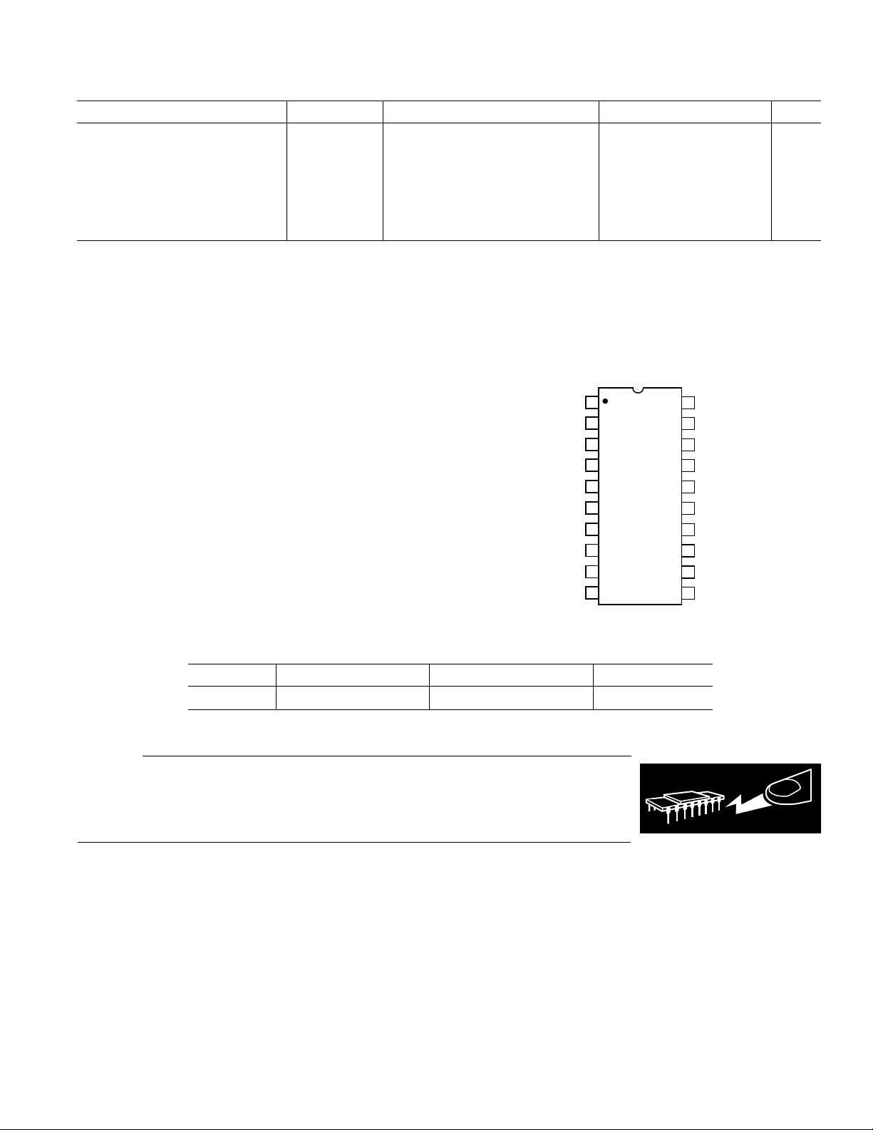
PIN CONFIGURATION
RU-20
VID4
1
2
VID3
3
VID2
4
VID1
FB
CT
5
6
7
8
9
10
ADP3164
TOP VIEW
(Not to Scale)
VID0
SHARE
COMP
GND
20
19
18
17
16
15
14
13
12
11
VCC
REF
PWM1
PWM2
PWM3
PWM4
PGND
CS–
CS+
PWRGD
CAUTION
ESD (electrostatic discharge) sensitive device. Electrostatic charges as high as 4000 V readily
accumulate on the human body and test equipment and can discharge without detection. Although
the ADP3164 features proprietary ESD protection circuitry, permanent damage may occur on
devices subjected to high-energy electrostatic discharges. Therefore, proper ESD precautions are
recommended to avoid performance degradation or loss of functionality.
REV. 0
–3–

ADP3164
PIN FUNCTION DESCRIPTIONS
Pin Mnemonic Function
1–5 VID4 – Voltage Identification DAC Inputs. These pins are pulled up to an internal 3 V reference, providing a
VID0 Logic 1 if left open. The DAC output programs the FB regulation voltage from 1.1 V to 1.85 V. Leaving all five
DAC inputs open results in the ADP3164 going into a “No CPU” mode, shutting off its PWM outputs.
6 SHARE Current Sharing Output. This pin is connected to the SHARE pins of other ADP3164s in multiple VRM systems
to ensure proper current sharing between the converters. The voltage at this output programs the output current
control level between CS+ and CS–.
7 COMP Error Amplifier Output and Compensation Point.
8 GND Ground. FB, REF, and the VID DAC of the ADP3164 are referenced to this ground. This is a low current ground
that can also be used as a return for the FB pin in remote voltage sensing applications.
9 FB Feedback Input. Error amplifier input for remote sensing of the output voltage.
10 CT External capacitor CT connection to ground sets the frequency of the device.
11 PWRGD Open drain output that signals when the output voltage is outside of the proper operating range or when a phase
is not supplying current even if the output voltage is in specification.
12 CS+ Current Sense Positive Node. Positive input for the current comparator. The output current is sensed as a voltage
at this pin with respect to CS–.
13 CS– Current Sense Negative Node. Negative input for the current comparator.
14 PGND Power Ground. All internal biasing and logic output signals of the ADP3164 are referenced to this ground.
15 PWM4 Logic-Level Output for the Phase 4 Driver.
16 PWM3 Logic-Level Output for the Phase 3 Driver.
17 PWM2 Logic-Level Output for the Phase 2 Driver.
18 PWM1 Logic-Level Output for the Phase 1 Driver.
19 REF 3.0 V Reference Output.
20 VCC Supply Voltage for the ADP3164.
ADP3164
VCC
REF
PWM1
PWM2
PWM3
PWM4
PGND
CS–
CS+
PWRGD
1.2V
20
19
20k⍀
18
17
16
15
14
13
12
11
+
V
FB
1F 100nF
12V
100⍀
100nF
5-BIT CODE
1
2
3
4
5
6
7
8
9
10
VID4
VID3
VID2
VID1
VID0
SHARE
COMP
GND
FB
CT
AD820
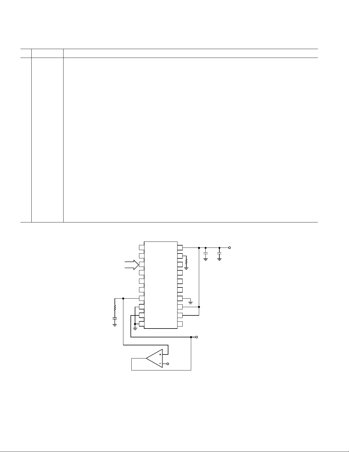
Figure 1. Closed-Loop Output Voltage Accuracy Test Circuit
–4–
REV. 0

Typical Performance Characteristics–ADP3164
10
1
FREQUENCY – MHz
0.1
0 10050
150 250200 300
CT CAPACITANCE – pF
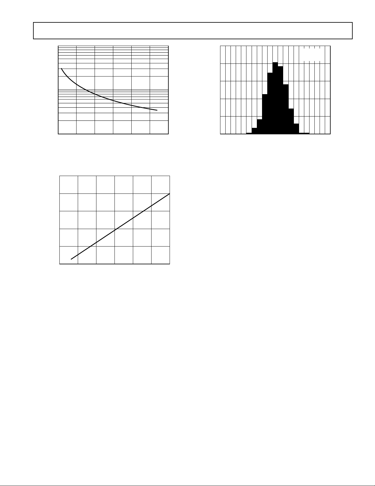
TPC 1. Oscillator Frequency vs. Timing Capacitor (CT)
4.5
4.4
4.3
25
20
15
10
NUMBER OF PARTS – %
5
0
–0.5
OUTPUT ACCURACY – % of Nominal
0 0.5
TPC 3. Output Accuracy Distribution
TA = 25ⴗC
V
= 1.6V
OUT
4.2
SUPPLY CURRENT – mA
4.1
4.0
0 1000500
OSCILLATOR FREQUENCY – kHz
1500 25002000 3000
TPC 2. Supply Current vs. Oscillator Frequency
REV. 0
–5–
 Loading...