5-Bit Programmable Synchronous
a
Controller for Pentium® III Processors
FEATURES
Active Voltage Positioning with Gain and Offset
Adjustment
Optimal Compensation for Superior Load Transient
Response
VRM 8.2, VRM 8.3 and VRM 8.4 Compliant
5-Bit Digitally Programmable 1.3 V to 3.5 V Output
Dual N-Channel Synchronous Driver
Total Output Accuracy ⴞ1% Over Temperature
High Efficiency, Current-Mode Operation
Short Circuit Protection
Overvoltage Protection Crowbar Protects Microprocessors
with No Additional External Components
Power Good Output
SO-16 Package
APPLICATIONS
Desktop PC Power Supplies for:
Pentium II and Pentium III Processor Families
AMD-K6 Processors
VRM Modules
GENERAL DESCRIPTION
The ADP3157 is a highly efficient synchronous buck switching
regulator controller optimized for converting the 5 V main supply into the core supply voltage required by the Pentium III and
other high performance processors. The ADP3157 uses an
internal 5-bit DAC to read a voltage identification (VID) code
directly from the processor, which is used to set the output
voltage between 1.3 V and 3.5 V. The ADP3157 uses a current
mode, constant off-time architecture to drive two external Nchannel MOSFETs at a programmable switching frequency that
can be optimized for size and efficiency. It also uses a unique
supplemental regulation technique called active voltage positioning to enhance load transient performance.
Active voltage positioning results in a dc/dc converter that meets
the stringent output voltage specifications for Pentium II and
Pentium III processors, with the minimum number of output
capacitors and smallest footprint. Unlike voltage-mode and
standard current-mode architectures, active voltage positioning
adjusts the output voltage as a function of the load current so that
it is always optimally positioned for a system transient.
The ADP3157 provides accurate and reliable short circuit protection and adjustable current limiting. It also includes an
integrated overvoltage crowbar function to protect the microprocessor from destruction in case the core supply exceeds the
nominal programmed voltage by more than 15%.
SD
ADP3157
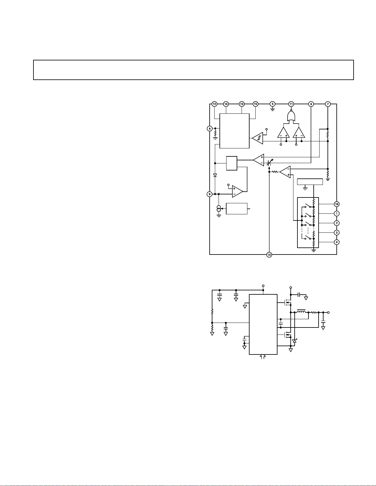
FUNCTIONAL BLOCK DIAGRAM
V
CMPI
SENSE–
REF
AGND
+15%
DELAY
V
REF
V
T1
+5% V
g
m
PWRGD
DRIVE1 DRIVE2 PGND
V
CC
NONOVERLAP
DRIVE
CROWBAR
IN
S
Q
R
V
T2
C
T
CMPT
OFF-TIME
CONTROL
ADP3157
CMP
V
+12V
CC
22mF
1mF
R1
R2
C
COMP
150pF
V
CC
DRIVE1
SD
ADP3157
SENSE+
CMP
SENSE–
DRIVE2
C
T
AGND
VID0–VID4
5-BIT CODE
PGND
V
1nF
Figure 1. 5-Bit Code Typical Application
+5V
IN
SENSE+
–5%
REF
V
REF
REFERENCE
1.20V
DAC
C
IN
+
L
R
SENSE
SENSE–
2R
R
V
1.3V TO
3.5V
+
C
O
VID0
VID1
VID2
VID3
VID4
O
Pentium is a registered trademark of Intel Corporation.
All other trademarks are the property of their respective holders.
REV. A
Information furnished by Analog Devices is believed to be accurate and
reliable. However, no responsibility is assumed by Analog Devices for its
use, nor for any infringements of patents or other rights of third parties
which may result from its use. No license is granted by implication or
otherwise under any patent or patent rights of Analog Devices.
One Technology Way, P.O. Box 9106, Norwood, MA 02062-9106, U.S.A.
Tel: 781/329-4700 World Wide Web Site: http://www.analog.com
Fax: 781/326-8703 © Analog Devices, Inc., 1999

ADP3157–SPECIFICATIONS
(0ⴗC ≤ TA ≤ +70ⴗC, V
= 12 V, VIN = 5 V, unless otherwise noted)
CC
1
Parameter Symbol Conditions Min Typ Max Units
OUTPUT ACCURACY
1.3 V Output Voltage V
O
(Figure 13) 1.283 1.3 1.317 V
2.0 V Output Voltage 1.980 2.0 2.020 V
3.5 V Output Voltage 3.465 3.5 3.535 V
I
OUTPUT VOLTAGE LINE ∆V
O
= 10 A (Figure 2)
LOAD
REGULATION VIN = 4.75 V to 5.25 V 0.05 %
INPUT DC SUPPLY CURRENT
Normal Mode I
Shutdown T
2
Q
VSD = 0.6 V 4.1 5.5 mA
= +25°C, VID Pins Floating 140 250 µA
A
CURRENT SENSE THRESHOLD
VOLTAGE V
SENSE(TH)VSENSE–
VID0–VID4 THRESHOLD VID
(TH)
Forced to V
– 3% 125 145 165 mV
OUT
Low 0.6 V
High 2.0 V
VID0–VID4 INPUT CURRENT I
VID0–VID4 PULL-UP RESISTANCE R
C
PIN DISCHARGE CURRENT I
T
OFF-TIME t
DRIVER OUTPUT TRANSITION t
VID
VID
12
OFF
, t
R
F
TIME T
POSITIVE POWER GOOD TRIP POINT3V
NEGATIVE POWER GOOD TRIP POINT3V
POWER GOOD RESPONSE TIME t
CROWBAR TRIP POINT V
PWRGD
PWRGD
PWRGD
CROWBAR
VID = 0 V 110 220 µA
20 30 kΩ
T
= +25°C
A
in Regulation 65 µA
V
OUT
V
= 0 V 2 10 µA
OUT
C
= 150 pF 1.8 2.45 3.2 µs
T
CL = 7000 pF (Drive 1, 2)
= +25°C 120 200 ns
A
% Above Output Voltage 5 8 %
% Below Output Voltage –8 –5 %
500 µs
% Above Output Voltage 9 15 24 %
ERROR AMPLIFIER
OUTPUT IMPEDANCE RO
ERR
275 kΩ
ERROR AMPLIFIER
TRANSCONDUCTANCE g
m(ERR)
2.2 mmho
ERROR AMPLIFIER MINIMUM
OUTPUT VOLTAGE V
CMPMIN
V
SENSE+
Forced to V
+ 3% 0.8 V
OUT
ERROR AMPLIFIER MAXIMUM
OUTPUT VOLTAGE V
CMPMAXVSENSE+
ERROR AMPLIFIER BANDWIDTH –3 dB BW
ERR
CMP = Open 500 kHz
Forced to V
– 3% 2.4 V
OUT
SHUTDOWN (SD) PIN
Low Threshold SD
High Threshold SD
Input Current SD
NOTES
1
All limits at temperature extremes are guaranteed via correlation using standard Statistical Quality Control (SQC) methods.
2
Dynamic supply current is higher due to the gate change being delivered to the external MOSFETs.
3
The trip point is for the output voltage coming into regulation.
Specifications subject to change without notice.
L
H
IC
Part Active 0.6 V
Part in Shutdown 2.0 V
10 µA
–2–
REV. A

ADP3157
TOP VIEW
(Not to Scale)
16
15
14
13
12
11
10
9
1
2
3
4
5
6
7
8
ADP3157
SENSE–
VID2
VID3
VID4
SD
AGND
SENSE+
C
T
CMP
PGND
DRIVE1
PWRGD
V
CC
DRIVE2
VID1
VID0
WARNING!
ESD SENSITIVE DEVICE
PIN FUNCTION DESCRIPTIONS
Pin No. Mnemonic Function
1–4, 16 VID1–VID4, Voltage Identification DAC Inputs. These pins are pulled up to an internal reference, providing a logic
VID0 one if left open. The DAC output programs the SENSE– regulation voltage from 1.3 V to 3.5 V. Leav-
ing all five DAC inputs open results in placing the ADP3157 into shutdown.
5 AGND Analog Ground. All internal signals of the ADP3157 are reference to this ground.
6 SD Shutdown. A logic high will place the ADP3157 in shutdown and disable both outputs. This pin is
internally pulled down.
7 SENSE– Connects to the internal resistor divider that senses the output voltage. This pin is also the (–) input
for the current comparator.
8 SENSE+ The (+) input for the current comparator. The output current is sensed as a voltage at this pin with
respect to SENSE–.
9C
T
10 CMP Error Amplifier output and compensation point. The voltage at this output programs the output cur-
11 PWRGD Power Good. An open drain signal indicates that the output voltage is within a ±5% regulation band.
12 V
CC
13 DRIVE2 Gate Drive for the (bottom) synchronous rectifier N-channel MOSFET. The voltage at DRIVE2
14 DRIVE1 Gate Drive for the buck switch N-channel MOSFET. The voltage at DRIVE1 swings from ground to
15 PGND Power Ground. The drivers turn off the buck and synchronous MOSFETs by discharging their gate
External capacitor CT connection to ground sets the off time of the device.
rent control level between the SENSE pins.
Supply Voltage to ADP3157.
swings from ground to V
V
.
CC
CC
.
capacitances to this pin. PGND should have a low impedance path to the source of the synchronous
MOSFET.
ABSOLUTE MAXIMUM RATINGS*
PIN CONFIGURATION
Input Supply Voltage (VCC) . . . . . . . . . . . . . . –0.3 V to +16 V
VID0–VID4, SD, PWRGD, CMP, C
DRIVE1, DRIVE2, SENSE+, SENSE– . . . . . . –0.3 V to V
. . . . . . . –0.3 V to V
T
CC
CC
Operating Ambient Temperature Range . . . . . . 0°C to +70°C
Junction Temperature Range . . . . . . . . . . . . . . 0°C to +150°C
θ
. . . . . . . . . . . . . . . . . . . . . . . . . . . . . . . . . . . . 110°C/W
JA
Storage Temperature Range . . . . . . . . . . . . –65°C to +150°C
Lead Temperature (Soldering, 10 sec) . . . . . . . . . . . .+300°C
*This is a stress rating only; operation beyond these limits can cause the device to
be permanently damaged.
ORDERING GUIDE
Temperature Package Package
Model Range Description Options
ADP3157JR 0°C to +70°C 16-Lead SOIC R-16A/SO-16
CAUTION
ESD (electrostatic discharge) sensitive device. Electrostatic charges as high as 4000 V readily
accumulate on the human body and test equipment and can discharge without detection.
Although the ADP3157 features proprietary ESD protection circuitry, permanent damage may
occur on devices subjected to high energy electrostatic discharges. Therefore, proper ESD
precautions are recommended to avoid performance degradation or loss of functionality.
REV. A
–3–

ADP3157
mP
SYSTEM
100kV
22V
ESR = 25mV EACH
2200mF 33
(25V)
22mF
ADP3157
1
VID1
2
VID2
3
VID3
4
VID4
5
AGND
6
SD
7
SENSE–
8
SENSE+
1nF
VID0
PGND
DRIVE1
DRIVE2
V
PWRGD
CMP
16
15
14
13
12
CC
11
10
9
C
T
C
T
200pF
R1
105kV
R2
18.2kV
1mF
C
COMP
3600pF
220V
IRL3803
IRL3803
L1
1.7mH
10BQ015
R
5mV
SENSE
220V
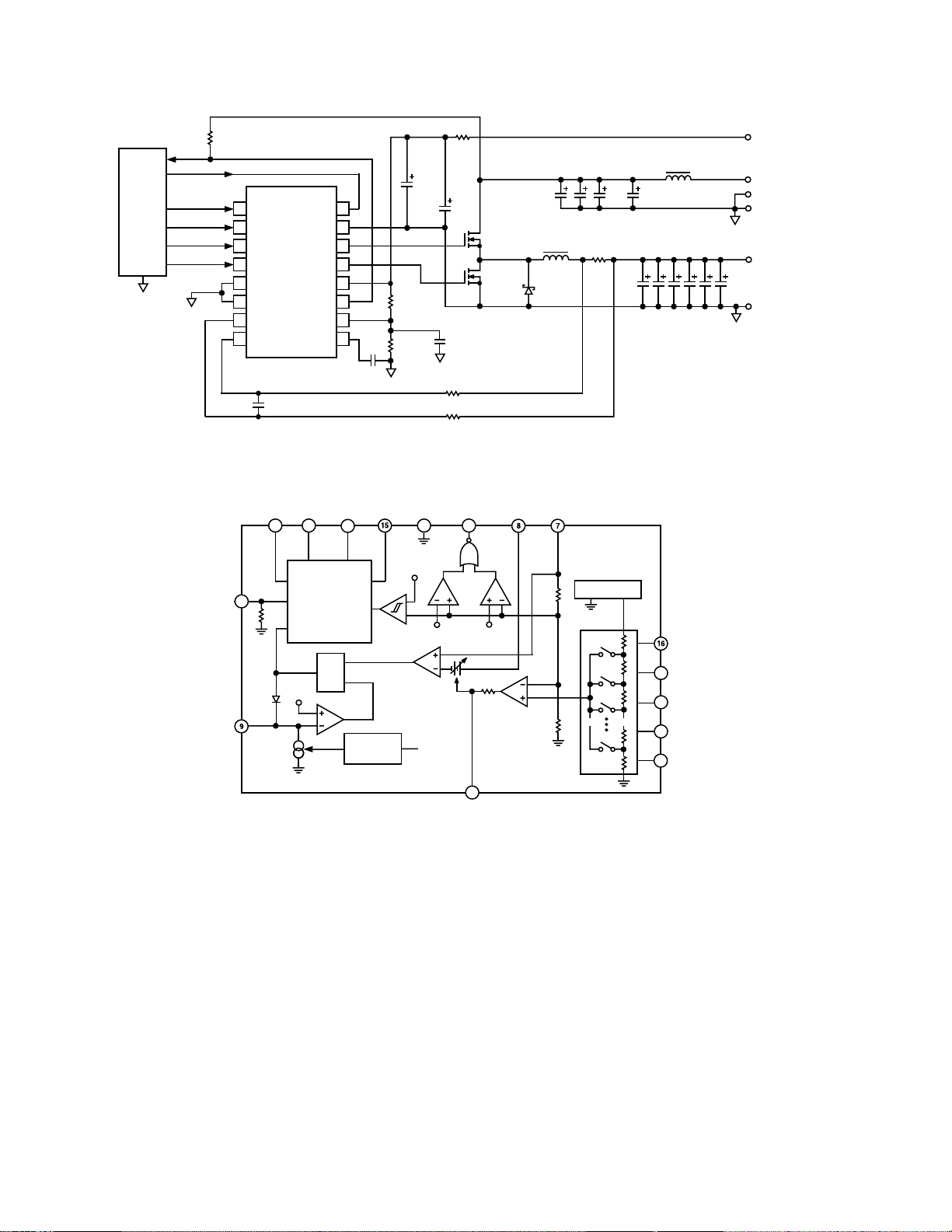
Figure 2. Typical VRM8.2/8.3/8.4 Compliant Core DC/DC Converter Circuit
SD
V
DRIVE1 DRIVE2 PGND
CC
14
12
NONOVERLAP
6
13
DRIVE
CROWBAR
IN
AGND PWRGD
5
V
+15%
REF
V
REF
+5% V
CMPI
S
Q
R
V
T2
CMPT
C
T
OFF-TIME
CONTROL
SENSE–
11
V
REF
T1
DELAY
–5%
SENSE+
g
m
2R
V
REF
SENSE–
ADP3157
REFERENCE
1.20V
R
DAC
L2
1mH
1mF
ESR = 25mV EACH
2200mF 3 6
(25V)
VID0
1
VID1
2
VID2
3
VID3
4
VID4
VCC +12V
VIN +5V
+5V RTN
+12V RTN
V
O
1.3V TO
3.5V
0-19A
RTN
10
CMP
Figure 3. Functional Block Diagram
–4–
REV. A
 Loading...