

a
SW
DRV
FB
IN
GND
COMP
ADP3088
V
OUT
1.8V
3.3H
10.0k
22.4k
20k
4.7pF
1N5817
IN
GND
10F
0.1F
220pF
V
IN
3.3V
10F
1 MHz, 750 mA Buck Regulator
ADP3088
FEATURES
1 MHz PWM Frequency
Automatic PWM to Power Saving Mode at Light Load
Fully Integrated 1 A Power Switch
3% Output Regulation Accuracy over Temperature,
Line, and Load
100% Duty Cycle Operation
Simple Compensation
Output Voltage: 1.25 V to 10.5 V
Small Inductor and MLC Capacitors
Low Quiescent Current while Pulse Skipping
Thermal Shutdown
Fully Integrated Soft Start
Cycle-by-Cycle Current Limit
APPLICATIONS
PDAs and Palmtop Computers
Notebook Computers
PCMCIA Cards
Bus Products
Portable Instruments
GENERAL DESCRIPTION
The ADP3088 is a high frequency, nonsynchronous PWM
stepdown dc-to-dc regulator with an integrated 1 A power switch
in a space-saving MSOP-8 package. It provides high efficiency
and excellent dynamic response and is very simple to use.
The ADP3088’s 1 MHz switching frequency allows for small,
inexpensive external components, and the current mode control
loop is simple to compensate and eases noise filtering. The device
operates in PWM current mode under heavy loads and saves
energy
at lighter loads by switching automatically into power
saving mode. Soft start is integrated completely on-chip, as is
cycle-by-cycle current limit.
the
Capable of operating from 2.5 V to 11 V input, the ADP3088 is
ideal for many applications, including portable, battery-powered
applications where local point-of-use power regulation is
required. Supporting output voltages down to 1.25 V, the
ADP3088 is ideal for generating low voltage rails, providing
the optimal solution in its class for delivering power efficiently,
responsively, and simply with a minimal printed circuit board area.
The device is specified over the industrial temperature range of
–40∞C to +85∞C.
COMP
GND
GND
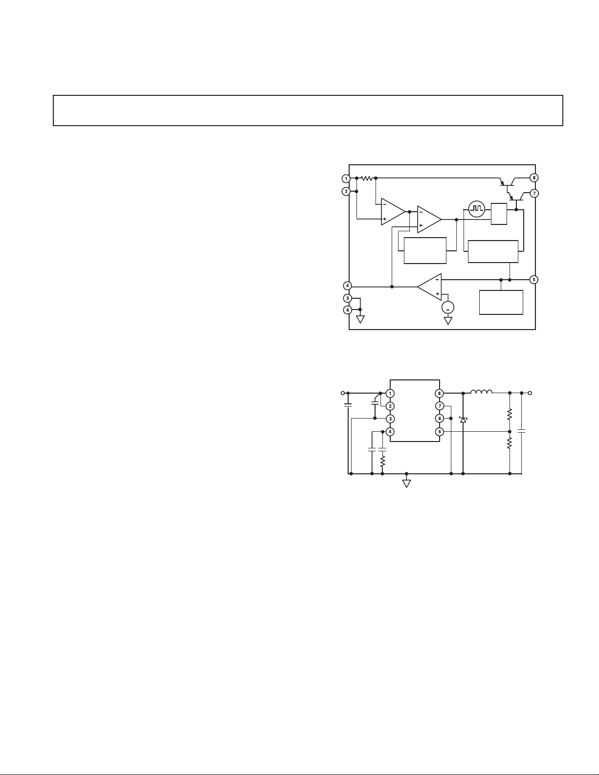
FUNCTIONAL BLOCK DIAGRAM
IN
IN
CURRENT
SENSE
AMP
PROTECTION
ADP3088
PWM
COMPARATOR
LOGIC
(ILI M, OT)
ERROR
AMP
g
m
+
REF
1.245V
1MHz
S
Q
R
RUN/STOP
COMPARATORS
SOFT START
TIMER
SW
DRV
FB
Figure 1. Typical Application
REV. C
Information furnished by Analog Devices is believed to be accurate and
reliable. However, no responsibility is assumed by Analog Devices for its
use, nor for any infringements of patents or other rights of third parties that
may result from its use. No license is granted by implication or otherwise
under any patent or patent rights of Analog Devices. Trademarks and
registered trademarks are the property of their respective owners.
One Technology Way, P.O. Box 9106, Norwood, MA 02062-9106, U.S.A.
Tel: 781/329-4700 www.analog.com
Fax: 781/326-8703 © 2004 Analog Devices, Inc. All rights reserved.

ADP3088–SPECIFICATIONS
Parameter Symbol Conditions Min Typ Max Unit
SUPPLY
Input Voltage Range V
Ground Current, Operating I
Quiescent Current, Operating I
Shutdown I
Thermal Shutdown Threshold T
OSCILLATOR
Oscillator Frequency f
Minimum Sleep Duty Cycle D
Maximum Duty Cycle D
Wake-Up Hysteresis V
OUTPUT SWITCH
Switch-On Voltage V
Current Limit Threshold I
Leakage Current VIN = 12 V 0.5 mA
ERROR AMPLIFIER
Reference Voltage Accuracy V
Reference Voltage Line FB = COMP, 0.02 %/V
Regulation V
Feedback Input Bias Current I
Sink/Source Current I
Short Circuit Current I
Transconductance gm,
MODULATOR
Transconductance gm,
Control Offset Voltage V
Soft Start Time t
Shutdown Threshold Voltage V
Slope Compensation m
NOTES
1
All limits at temperature extremes are guaranteed via correlation using standard Statistical Quality Control (SQC).
2
For higher efficiency operation, tie the DRV pin to the output for IL < 250 mA and VIN > 3 V.
3
VIN – VSW includes voltage drop across internal current sensor.
Specifications subject to change without notice.
IN
2
GND
Q
SD
SD
SW
PSM
MAX
HYST
3
IO
LIM
REF
FB
COMP
COMP, SD
EA
MOD
PWM, OS
SS
COMP, SD
SC
(VIN = 3.3 V, TA = –40C to +85C, unless otherwise noted.)
DRV = GND 2.5 11 V
VIN = 10 V, IL = 500 mA,
DRV = GND 6 mA
DRV = 2 V 2.5 3.6 mA
No Load 150 250 mA
V
= 0 V 15 40 mA
COMP
160 ∞C
0.75 1 1.25 MHz
IL = 500 mA 14 %
100 %
FB Voltage Drops below V
REF
20 30 40 mV
IL = 500 mA, FB = GND, and 0.25 0.4 V
DRV = GND
1.0 1.2 1.4 A
FB = COMP 1.222 1.245 1.265 V
= 3 V to 12 V
IN
Soft Start Expired –50 +1 +50 nA
35 60 85 mA
V
= 0 V, Activating 20 40 mA
COMP
Shutdown
FB = COMP 480 mA/V
V
COMP
to I
L
1 A/V
0.90 V
250 600 ms
340 750 mV
Effectively Summed to I
SW
0.7 A/ms
1
–2–
REV. C
ADP3088
ABSOLUTE MAXIMUM RATINGS *
Input Supply Voltage . . . . . . . . . . . . . . . . . . . –0.3 V to +12 V
Voltage on Any Pin with Respect to GND . . . –0.3 V to +12 V
(Voltage on Any Pin May Not Exceed V
)
IN
Operating Ambient Temperature Range . . . . –40∞C to +85∞C
Operating Junction Temperature . . . . . . . . . . . . . . . . . . 125∞C
(4-Layer Board) . . . . . . . . . . . . . . . . . . . . . . . . . . 116∞C/W
q
JA
qJA (2-Layer Board) . . . . . . . . . . . . . . . . . . . . . . . . . . 159∞C/W
Storage Temperature Range . . . . . . . . . . . . –65∞C to +150∞C
Lead Temperature Range (Soldering 10 sec) . . . . . . . . . 300∞C
Vapor Phase (60 sec) . . . . . . . . . . . . . . . . . . . . . . . . . 215∞C
Infrared (15 sec) . . . . . . . . . . . . . . . . . . . . . . . . . . . . 220∞C
*Stresses above those listed under Absolute Maximum Ratings may cause permanent
damage to the device. This is a stress rating only and functional operation of the
device at these or any other conditions above those listed in the operational sections
of this specification is not implied. Exposure to absolute maximum rating conditions
for extended periods may affect device reliability. Only one absolute maximum
rating may be applied at any one time.
ORDERING GUIDE
Temperature Package
Model Range Option Branding
ADP3088ARM-REEL –40∞C to +85∞CMSOP-8 P0A
ADP3088ARM-REEL7 –40∞C to +85∞CMSOP-8 P0A
PIN CONFIGURATION
8
SW
7
DRV
6
GND
5
FB
GND
COMP
1
IN
2
IN
3
4
ADP3088
TOP VIEW
(Not to Scale)
PIN FUNCTION DESCRIPTIONS
Pin No. Mnemonic Function
1, 2 IN Power Supply Input. Both pins must
be connected.
3, 6 GND Ground. Both pins must be
connected.
4 COMP Feedback Loop Compensation and
Shutdown Input. An open drain or
collector used to pull the pin to
ground will shut down the device.
5FB Feedback Voltage Sense Input. This
pin senses the voltage via an external
resistor divider.
7 DRV This pin provides a separate path for
the drive current to be connected to
ground.
8SWSwitching Output.
CAUTION
ESD (electrostatic discharge) sensitive device. Electrostatic charges as high as 4000 V readily
accumulate on the human body and test equipment and can discharge without detection. Although the
ADP3088 features proprietary ESD protection circuitry, permanent damage may occur on devices
subjected to high energy electrostatic discharges. Therefore, proper ESD precautions are recommended
to avoid performance degradation or loss of functionality.
REV. C
–3–
ADP3088
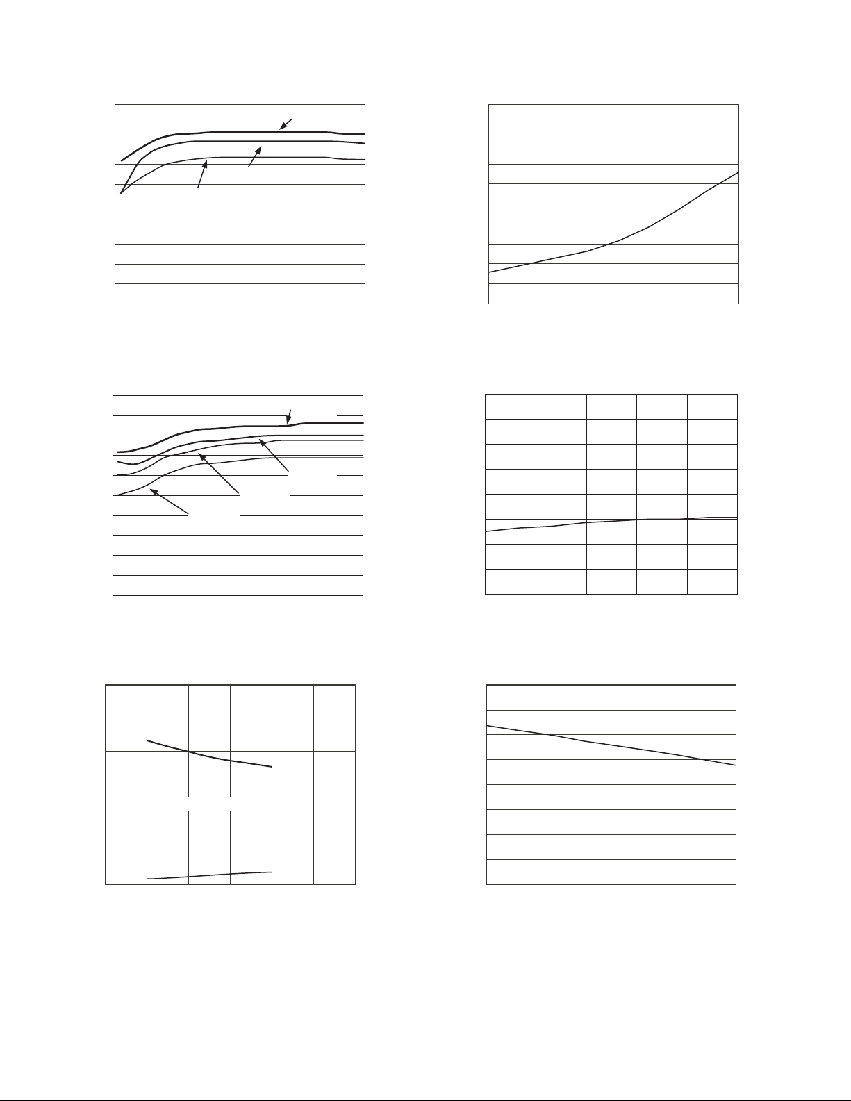
–Typical Performance Characteristics
100
90
80
70
60
50
40
EFFICIENCY (%)
30
VIN = 5V, CIN = C
20
TA = 25C
10
0
0 500100 200 400300
V
OUT
V
OUT
= 1.5V
OUT
= 10F, L = 10H
LOAD CURRENT (mA)
= 2.5V
V
= 3.3V
OUT
TPC 1. Efficiency vs. Load Current and Output Voltage
100
90
80
70
60
50
40
EFFICIENCY (%)
30
20
10
0
V
OUT
V
= 1.5V
OUT
VIN = 10V, CIN = C
TA = 25C
0 500100 200 400300
= 10F, L = 10H
OUT
LOAD CURRENT (mA)
= 2.5V
V
= 5V
OUT
V
= 3.3V
OUT
TPC 2. Efficiency vs. Load Current and Output Voltage
200.00
180.00
160.00
140.00
120.00
STANDBY QUIESCENT CURRENT (A)
100.00
–40 85–15 10 6035
TEMPERATURE (C)
TPC 4. Standby Quiescent Current vs. Temperature
5.00
4.00
I
= 500mA
3.00
GROUND CURRENT (mA)
2.00
1.00
LOAD
V
= 2V
DRV
–40 85–15 10 6035
TEMPERATURE (C)
TPC 5. Ground Current vs. Temperature
100
IL = 500mA
10
V
= 1.5V, CIN = C
OUT
TA = 25C
1
QUIESCENT CURRENT (mA)
0
01024 86
= 10F, DRV = GND
OUT
IL = 0mA
INPUT VOLTAGE (V)
TPC 3. Quiescent Current vs. Input Voltage
1.2438
1.2433
1.2428
FEEDBACK VOLTAGE (V)
1.2423
1.2418
12
–40 85–15 10 6035
TEMPERATURE (C)
TPC 6. Feedback Voltage vs. Temperature
–4–
REV. C
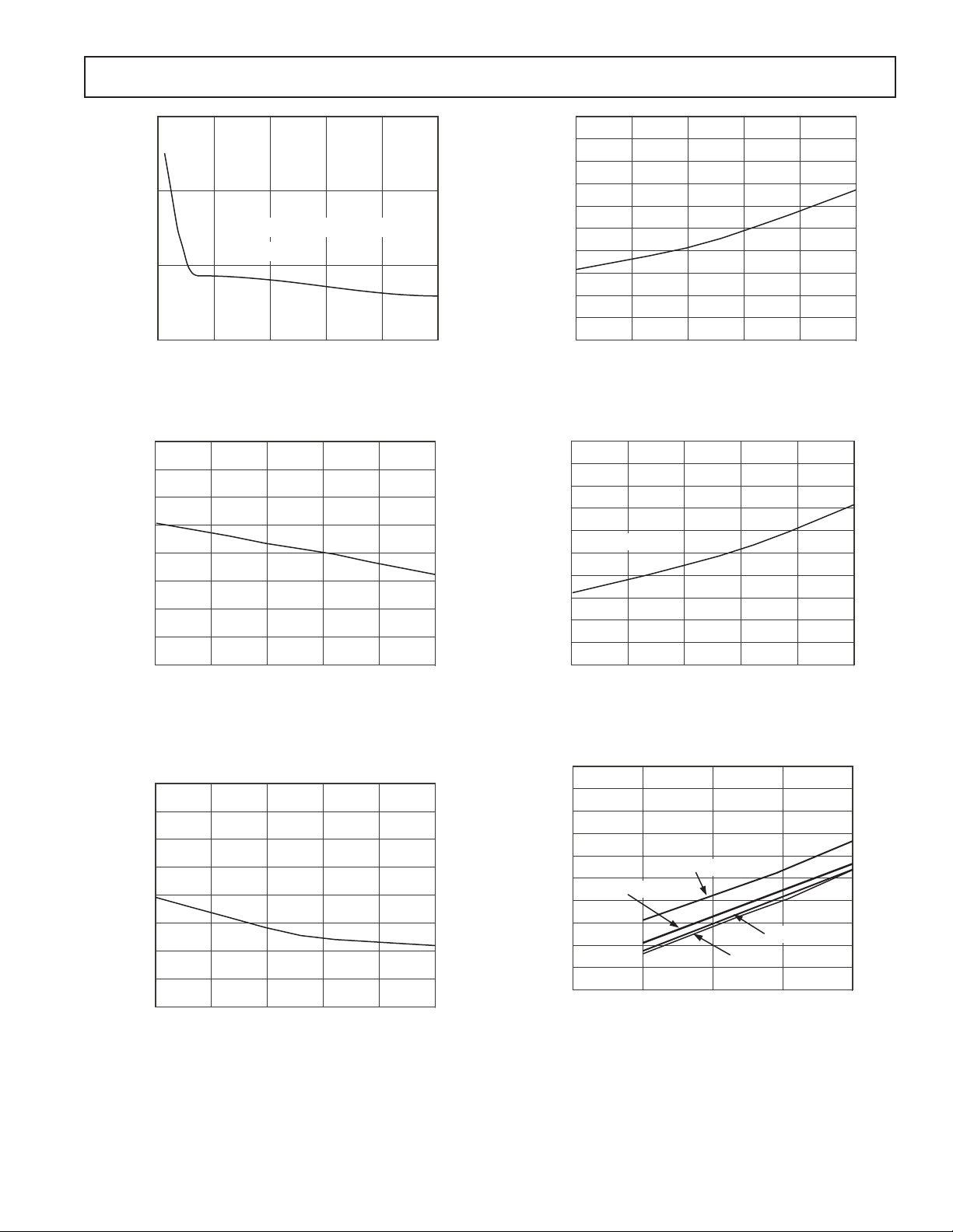
1.515
12.00
–40 85–15 10 6035
TEMPERATURE (C)
14.00
16.00
18.00
SHUTDOWN SUPPLY CURRENT (A)
20.00
10.00
0.220
–40 85–15 10 6035
TEMPERATURE (C)
0.240
0.260
0.280
SWITCH VOLTAGE (V)
0.300
0.200
I
LOAD
= 500mA
0.400
0.00 1.000.25 0.50 0.75
OUTPUT CURRENT (A)
0.500
0.600
0.900
SWITCH SATURATION VOLTAGE (V)
1.000
0.300
0.700
0.800
0.100
0.200
V
IN
= 2.5V
V
IN
= 5V
V
IN
= 12V
V
IN
= 3.3V
TA = 25C
1.505
ADP3088
1.495
OUTPUT VOLTAGE (V)
1.485
0 500100 200 400300
TPC 7. Load Regulation
1.10
1.05
1.00
FREQUENCY (MHz)
0.95
0.90
–40 85–15 10 6035
VIN = 5V, CIN = C
TA = 25C
OUTPUT CURRENT (mA)
TEMPERATURE (C)
= 10F, L = 10H
OUT
TPC 10. Shutdown Supply Current vs. Temperature
TPC 8. Oscillator Frequency vs. Temperature
1.20
1.15
1.10
CURRENT LIMIT (A)
1.05
REV. C
1.00
–40 85–15 10 6035
TPC 9. Current Limit vs. Temperature
TEMPERATURE (C)
TPC 11. Switch-Sense Resistor Voltage vs. Temperature
TPC 12. Switch Saturation Voltage
vs.
Load
Current and Input Voltage
–5–

ADP3088
CH 1: INPUT VOLTAGE, 2V/DIV
2: OUTPUT VOLTAGE, 500mV/DIV
CH
CH 1: INPUT VOLTAGE, 10mv/DIV,
AC-COUPLED
VIN = 5V, V
C
IN
T
A
= 1.5V, LOAD CURRENT = 0mA,
OUT
= C
= 10F, L = 10H
OUT
= 25C
TPC 13. Start-Up Waveform
CH 1: INPUT VOLTAGE, 2V/DIV
CH 2: OUTPUT VOLTAGE, 500mV/DIV
VIN = 5V, V
= C
C
IN
= 25C
T
A
= 1.5V, LOAD CURRENT = 500mA,
OUT
= 10F, L = 10H
OUT
TPC 14. Start-Up Waveform
TA = 25C
V
= 5V, V
IN
VIN = 5V, V
= C
C
IN
TA = 25C
OUT
= 1.5V, LOAD CURRENT = 500mA,
OUT
= 10F, L = 10H
OUT
TPC 16. V
= 1.5V, LOAD CURRENT = 10mA, CIN = C
OUT
Ripple
= 10F, L = 10H
OUT
TPC 17. Power-Saving Mode Waveforms*
CH 1: INPUT VOLTAGE, 2V/DIV
CH 2: OUTPUT VOLTAGE,
500mV/DIV
V
IN
C
IN
= 2.5V, V
= C
= 1.25V, LOAD CURRENT = 250mA,
OUT
= 10F, L = 10H, TA = 25C
OUT
TPC 15. Start-Up Waveform
*NOTES FOR TPCs 17 AND 18
CH 1: Output Voltage, 20mV/DIV, AC-Coupled
CH 2: Switch Node Voltage, 2V/DIV
CH 3: Inductor Current, 100mA/DIV
–6–
TA = 25C
V
= 5V, V
IN
= 1.5V, LOAD CURRENT = 25mA,
OUT
C
= C
= 10F, L = 10H
IN
OUT
TPC 18. Steady-State Waveforms*
REV. C

CH 1: LOAD CURRENT STEP, 167mA/DIV
CH 2: OUTPUT VOLTAGE, 100mV/DIV
ADP3088
VIN = 5V, V
=
T
A
= 1.5V, LOAD CURRENT = 100mA,
OUT
25C
, CIN = C
= 10F, L = 10H
OUT
TPC 19. Steady-State Waveforms*
CH 1: LOAD CURRENT STEP, 167mA/DIV
CH 2: OUTPUT VOLTAGE, 100mV/DIV
= 5V, V
V
IN
T
= 25C,
A
= 1.5V, LOAD CURRENT = 50mA TO 550mA,
OUT
CIN = 10F, C
= 20F, L = 10H
OUT
TPC 20. Load Transient Response
VIN = 5V, V
T
A
= 1.5V, LOAD CURRENT = 50mA TO 550mA TO 50mA,
OUT
= 25C, CIN = 10F, C
= 20F, L = 10H
OUT
TPC 22. Load Transient Response
CH 1: INPUT VOLTAGE, 2V/DIV
CH 2: OUTPUT VOLTAGE, 20mV/DIV
VIN = 3V TO 5V, V
= 25C, CIN = 10F, C
T
A
= 1.5V, LOAD CURRENT = 500mA,
OUT
= 10F, L = 10H
OUT
TPC 23. Line Transient Response
CH 1: LOAD CURRENT STEP, 167mA/DIV
CH 2: OUTPUT VOLTAGE, 100mV/DIV
VIN = 5V, V
= C
C
IN
T
= 25C
A
= 1.5V, LOAD CURRENT = 550mA TO 50mA,
OUT
= 10F, L = 10H
OUT
TPC 21. Load Transient Response
*NOTES FOR TPC 19
CH 1: Output Voltage, 20mV/DIV, AC-Coupled
CH 2: Switch Node Voltage, 2V/DIV
CH 3: Inductor Current, 100mA/DIV
REV. C
–7–

ADP3088
THEORY OF OPERATION
The ADP3088 is a fixed frequency buck switching regulator in
an MSOP-8 package using an external Schottky rectifier. It
features an integrated 1 A power switch and switches at 1 MHz.
The ADP3088 uses PWM operation and incorporates soft start
for controlled start-up sequence and overtemperature switch
protection. The ADP3088 draws low current while running
in power saving mode and even lower current in shutdown.
The system shown in the Functional Block Diagram is configured for a 1.8 V output using a 10 mH inductor. At the beginning
of a cycle, the 1 MHz oscillator enables an SR latch, enabling the
internal 1 A power switch. The current sense amplifier and the
protection logic block monitor the current flowing between the
IN and SW pins. The switch is turned off when the current
reaches a level determined by the protection logic block or
PWM comparator, whichever is lower. The error amplifier
measures the output voltage through an external resistor divider
tied to the FB pin. This amplifier servos the switch current to
regulate the FB pin voltage to 1.245 V. An internal regulator
provides power to the control circuitry. The COMP pin can be
used to shut down the ADP3088. When pulled low, it turns off
the internal regulator, thus biasing down the chip, reducing the
input current, and disconnecting the output from the input.
Antisaturation circuitry is used to drive the switch to the edge of
saturation. This allows the driver to quickly switch at 1 MHz
and maintain good efficiency. For improved efficiency, the DRV
pin may be connected to the output provided that the input
voltage is at least 1 V greater than the output.
If the output load increases, the error amplifier will detect a
lower voltage on the FB pin via the resistor divider on the output
and send a signal to the PWM comparator to increase the on time
of the switch. This in effect increases the duty cycle and provides
more current to drive the increased load during the transient
event until a new operating point is established.
Reference
The ADP3088 incorporates an internal band gap reference,
including curvature correction for an extremely low temperature
coefficient. The reference can be disabled by grounding the
COMP pin, which also turns off the bias for the rest of the chip.
Error Amplifier
The error amplifier provides a control voltage to the PWM stage
to set the peak inductor current that sets the output current of
the regulator. It is a g
the COMP pin.
Protection Logic
The protection logic block provides current limit and
overtemperature protection. The overtemperature protection is
enabled when the temperature of the chip exceeds a specified
preset temperature; the switch will be disabled until the temperature drops below a specified level, then normal operation will
resume. The thermal shutdown only stops switching, but it does
not put the chip into power saving mode, nor does it reinitiate soft
start. As the chip cools slightly, it will rapidly cycle in and out of
thermal shutdown, maintaining the die temperature at 160∞C but
allowing the output voltage and current to swing up and down.
amplifier in that its output is a current to
m
The current limit protection overrides the PWM comparator; if
this occurs, then the switch pulse will be terminated and the soft
start mode will be reset.
Current Sense Amplifier
The voltage on the internal current sense resistor is sensed and
passed to the ramp input of the PWM comparator. This current
sense signal is also passed to the current limit comparator for
peak current limit shutdown. At the current limit, the soft start
capacitor is reset and soft start is reinitiated. The current limit is
nominally 1.2 A. Slope compensation is added to the ADP3088
to stabilize the loop. A generated ramped signal is summed with
the current sense signal to provide slope compensation. Slope
compensation is needed to close the inner loop so subharmonic
oscillation is avoided. The ramp is reset with each clock cycle so
that the ADP3088 is capable of true 100% duty cycle.
Run/Stop Comparators
This block creates the 1 MHz signal sent to the SR latch that is
used for the switching frequency. It also takes the FB voltage
and decides when to go into wake-up mode from power saving
mode. The decision to induce the power saving mode is based
on the duty ratio. During steady-state continuous operation, the
duty ratio of a PWM buck regulator is simply a function of the
input/output voltage ratio, with second-order effects including
the voltage drop of the internal switch and the external diode.
Once the load drops to a certain point, discontinuous operation
occurs, and the duty ratio begins to modulate to maintain
regulation. In the ADP3088, the regulator goes to sleep when
the integrated duty ratio measurements drop to less than half of
the minimum expected integrated duty ratio. The minimum
expected duty ratio occurs at the maximum input voltage and
the minimum output voltage in continuous mode operation.
PWM Comparator
The PWM comparator looks at the signal from the current
sense amplifier and the error amplifier to determine the correct
switch-on time to regulate the output voltage under a given load.
Soft Start Timer
The soft start will prevent saturating the inductor, which could
cause uncontrolled overshoot of the output voltage and electrical
stress to the system at startup. When first powered up, an internal
soft start capacitor is discharged and the soft start circuitry
provides a gradually decaying offset to the error amplifier to
prevent it from saturating and from commanding the maximum
switch current to charge the output capacitor. The output
voltage approaches the final regulation voltage with a smooth
exponential decay. This will reduce electrical stress to the system.
Output
The output stage contains the bipolar power switch and the
circuits necessary to switch it on and off quickly. The pass
switch is driven to the edge of saturation, and the result is a fast
switching response and low switch resistance. For improved
efficiency, the DRV pin may be connected to the output, pro
that the input voltage is at least 1 V higher than the
vided
output.
This will send the current needed to drive the bipolar switch to
the output load instead of routing it to ground. For some V
and I
configurations, the DRV pin must be grounded for
LOAD
IN
reliable operation.
–8–
REV. C

ADP3088
APPLICATION INFORMATION
Output Voltage Setting
In its standard usage, the output voltage of the ADP3088 is
programmed to a desired fixed value by a resistor divider from
the output voltage into the feedback node, the FB pin, at which
node the control loop ensures regulation at the reference level,
. The divider should be designed to satisfy the formula
V
REF
VV
=¥+
OUT REF
Ê
1
Á
Ë
ˆ
R
A
˜
R
¯
B
(1)
where RA is the upper divider resistor (between the output and FB)
is the lower one (between FB and ground). RA and R
and R
B
B
are recommended to have values in the range of 2 kW~200 kW and
are likely to require a 1% tolerance or better to attain acceptable
output voltage tolerance.
In less conventional applications described separately, the resistor
feedback configuration can be modified or tapped with other
resistors to affect current flow into the FB node that, in turn,
influences the output voltage. Even a switched voltage can be
summed into the FB node as long as it is sufficiently integrated
and does not intolerably compromise the transient response. This
latter application is considered further below, for an application for
powering a DSP.
Input Voltage, Power Dissipation Considerations, and Power Savings Mode
The input voltage range is not typically considered a critical
parameter for electrical functionality, but there are several
considerations, upon which there is further elaboration below:
1. V
must never exceed the maximum rated voltage.
IN
2. V
must be within the specified operating range when normal
IN
operation is expected.
3. V
must be greater than V
IN
by at least the specified head-
OUT
room when dc regulation is expected.
4. V
, if not sufficiently greater than V
IN
, may limit the large
OUT
signal transient response of a buck converter.
5. V
, if much greater than V
IN
, may give rise to such a low
OUT
duty ratio that it activates power savings mode even at static
higher load conditions or upon dynamic load changes when
it is not desired.
6. V
affects the device power dissipation (a lower value causes
IN
higher dissipation), which in turn affects die temperature
that must be kept below a maximum rating.
The lowest input voltage together with the maximum output
voltage and maximum current create the conditions for the
maximum power dissipation in the device, which determine the
maximum temperature rise that should be checked against the
maximum junction temperature rating. The formula for maximum
power dissipation in the device is given by
VV
+
@,
P
DMAX
OFIOMAX
=
V
IV
¥¥
,@,
IN
OMAX SW IO MAX
(2)
where VF is the diode forward voltage drop and VSW is the drop
across the internal switch and current sensing resistor that
appears between the V
and SW pins of the ADP3088 during the
IN
on state of the switch. Both of these variables can be approximated
from a combination of worst-case specifications and typical graphs.
Multiply the power dissipation by the thermal resistance from
junction to case or ambient, as desired, to determine the internal
temperature rise.
If the input voltage were so much higher than the output voltage
that it required an average duty ratio less than an internally
preset threshold, then power savings mode (PSM)—which is
characterized by periodic shutdown and wake-up of the device
that reduces average quiescent current—would be active for all
load conditions rather than only at lighter loads, for which it is
intended. PSM operation is characterized by low frequency
ripple on the output that appears similar to the behavior of a
hysteretic regulator. This is usually not a factor for consideration and may be ignored if PSM operation is acceptable for all
load conditions. But in case it is relevant, the following recommendation is offered:
VV
+
IN
<
D
OF
()
PSM MAX
(3)
V
It is not possible to prevent the duty ratio from tending toward
zero in nonsynchronous buck converters below a certain minimum
load current level called “borderline current” or “critical current”
for the power converter. That corresponds to the inductor
ripple current reaching zero at its bottom peak, sometimes called
the “valley current.” If PSM activation strains the lower regulation
limit due to the hysteretic ripple, the output voltage can be offset
slightly upward by readjusting the nominal voltage setpoint with
the resistor divider.
Even though a buck converter may have a low dropout voltage
that allows the static regulation to be maintained as the input
voltage drops near the output voltage, in buck converters, the
slew rate limitation of the inductor current can compromise the
dynamic regulation in response to the load current step increases.
That is because the maximum rate the current can be increased
to in the inductor is proportional to the voltage available to
impress across it, which is compromised as the input voltage
reduces toward the output voltage. This is not a limitation of
the device but of buck converters in general. The limitation is
considered part of the output filter design, although it could
also be considered in terms of a minimum acceptable input
voltage for a given output filter that will ensure that the dynamic
response is acceptably maintained.
Output Filter Components
In most applications, it is desirable to use the smallest inductor
value that does not introduce practical problems, since this tends
to yield the lowest cost inductor. One reason for using an even
larger inductor than the minimum tolerable might be to reduce
the output ripple voltage further. But cost being equal, this is
generally better accomplished with a better quality or proportionally larger output capacitor instead, since a larger inductor
degrades the large signal transient performance capability.
A conservative nominal design target value for the inductor of a
typical application circuit is that which creates a peak-to-peak
ripple current, DIL, for the nominal input voltage that is approximately a third of the nominal 500 mA rating of the ADP3088.
The reason for not basing the ripple current on the maximum
load current is concern about the protection. Scaling the ripple
currents with lower load currents would yield higher inductor
values that might give satisfactory operation. However, in order for
overload operation up to the current limit level of the ADP3088
to be satisfactory, it would be necessary to choose an inductor
REV. C
–9–

ADP3088
rated up to that higher current, which would likely yield an
unsatisfactory inductor size and cost. In any case, having chosen
a target level for DI
, the recommended inductor value is
L
given by
DVV
-¥ +
()( )1
L
=
OF
fI
¥
D
SW L
(4)
where D is the duty ratio, the suffix indicating continuous
inductor current, and is given by
VV
+
D
OF
=
VVV
+-
IN F SW
(5)
VSW and VF are assessed at full load, and fSW is the fixed
switching frequency of the ADP3088. The formula suggests the
calculation of L using a nominal input voltage; for applications
requiring a large range of V
response at V
versus the higher ripple at V
IN(MIN)
, the limitations of transient
IN
IN(MAX)
may
warrant deeper consideration of how to optimize the design. In
applications where load transients are not severe, this conservative
design for L is recommended. A more aggressive minimization of
L is outlined below, but a few restrictions are noted.
As inductance becomes smaller, the ripple current becomes
larger. If the ripple becomes particularly large or, as an additional factor, if the load is particularly dynamic, then there is
an increasing possibility that the peak inductor current will
reach the current limit shutdown threshold, I
, which is not
CL
desirable. This should be avoided by restricting the minimum
inductor value to keep the ripple current moderated. An
alternative way to prevent excessive dynamic overshoot of the
inductor current during a load transient is to reduce the dc
gain of the error amplifier by adding resistive feedback; this
idea is discussed below.
Another important restriction of the minimum inductor value may
apply. The design should ensure against possible subharmonic
oscillation that can occur in all fixed frequency, current-controlled
switching power supplies when switching at high duty ratios.
The subharmonic oscillation phenomenon will not be explained
here (there are many papers written on the subject) except to
say that it is characterized by alternating high and low duty
ratios, i.e., every other cycle, which produces additional ripple
on the output. To prevent subharmonic oscillation, the following restriction for the minimum inductor value is recommended:
H
m
L
>¥+
VV
()
V
OF
The value used for V
VV
+2
OF
¥
V
IN MIN
should be only the minimum input
IN(MIN)
035
– .
()
(6)
voltage for which normal high performance operation must be
ensured. Note that the value returned for L may be negative, in
which case the restriction does not apply. If the preceding formula
yields a lower inductor value than the conservative recommendation given previously, as is likely for most applications, then
one should consider further limitations to see how low the value
can be minimized.
For a given inductor selection, the earlier formula is rearranged
for convenience and skewed to the worst-case input voltage to
determine the maximum inductor ripple current, DI
DI
LMAX
=
()
VVV
IN MAX O SW
()
VVV
IN MAX F SW
()
–
-
–
+
VV
+
OF
¥
fL
¥
SW
.
L
(7)
Performance degradation of the inductor, consisting of some
loss of inductance or excessive power loss, may be encountered
at higher ripple currents, so the ripple current figure, together
with the knowledge of the expected dc current, should be
checked against the specifications of the inductor.
If the ESR of the output capacitor is substantial, as it is likely to
be if an MLC capacitor is not used, then the ripple voltage on
the output, dominated by the ESR, may be substantial and of
concern for regulation specifications. The resistive component
of the output voltage ripple is simply the ripple current multiplied by the ESR, and if it is more than a few millivolts, it will
dominate the output capacitance in contributing to the output
ripple voltage.
The boundary condition of the inductor reaching the borderline
current, I
I
OBL
, can be determined by the formula
O(BL)
VV
OFSWIN O SW
=
()
fL
VVV
+
¥
VVV
-+-2
IN F SW
(8)
Below this output current level, the inductor current will be
discontinuous, and the duty ratio will be modulated to lower
values by factors substantially more than the losses that cause
only a small amount of the modulation in the continuous inductor
current operation. PSM is initiated automatically by a proprietary technique consisting of a duty ratio amplifier with an
internal time constant. As the load current drops well into the
low current region and the duty ratio passes below the threshold
of D
for a sufficient time, PSM is activated. The correspond-
PSM
ing level of output current is given by
VVV
1
=¥
2
2
ID
O(PSM) PSM
+-
IN F SW
VV
OF
+
VVV
--
IN O SW
¥
L
f
¥
SW
(9)
It can be seen in the formula that this current threshold is inversely
proportional to inductance, so although it is usually not a relevant
concern, it is noted that an aggressively low output inductance
should be avoided to keep the PSM threshold current at a desirably low level.
For the user’s reference, when current is below the borderline
level, the duty ratio is modulated according to the formula
DI
=¥¥
2
DO
VVV
IN F SWSWIN O SW
VV
+
OF
+-
fL
¥
VVV
¥
--
(10)
where the suffix indicates that the inductor current is discontinuous.
For controlling the capacitive component of the output ripple
voltage, the following constraint on the minimum output
capacitance should be applied:
I
D
>
fV
SW R
L
D8
(11)
C
O
–10–
REV. C

ADP3088
where ⌬VR is the tolerable ripple voltage. However, this constraint
is rarely relevant, since the typical capacitance requirement is
driven more by dynamic response requirements than by ripple
concerns. In a typical application circuit, a 10 mF capacitor
produces a capacitive output voltage ripple component of only
about 2 mV. 10 mF is usually sufficient for applications that do not
impose particularly high frequency load transients, and imposes
additional constraints that are elaborated upon in the next section.
Load Characterization
Optimization of the compensation, as well as the output filter,
requires some knowledge of a fundamental characteristic of the
load. Qualitatively, there are two types of loads with which we
are concerned: fast slew rate and slow slew rate. These slew
rates are assessed with respect to the minimum (absolute)
inductor (current) slew rate, as given by
È
Ê
ˆ
dI
L
Í
Á
˜
dt
Ë
¯
Í
Î
,
MIN
˘
Ï
VVV
IN MIN SW O
=<
˙
Ì
˙
Ó
˚
--
()
L
MAX
and
+
VV
OF
L
MAX
¸
˝
˛
(12)
where the < sign indicates a selection of whichever bracket term
is lower.
If the slew rate of the load is fast compared to the minimum
inductor slew rate, then the ability of the power converter to
contain the output voltage deviation following a load change is
limited not only by the response of the control loop, i.e., by its
speed to demand zero or maximum duty ratio from the modulator,
but by the power stage as well. In such a case, beginning with
the recognition that output voltage deviation would be substantial
even if the loop response were instantaneous, it can be shown
that one can achieve better overall voltage containment by
degenerating the dc loop gain. As a technical matter, it should be
noted that there will always be some minimum output voltage
deviation downward due to a load step even if the inductor slew is
as fast as the load slew rate. During a switching cycle, the modulator latches its “decision” to turn off the switch. It cannot rescind
that decision, but must instead wait for the next clock cycle to
turn on the switch again and begin slewing the inductor current
upward. This is only a second-order consideration.
Slow slew rate loads may be referred to simply as conventional
loads, since these have been the more prevalent type of load.
Optimally compensating a conventional load is synonymous
with small signal ac considerations; the objective is to maximize
the ac gain up to the crossover frequency, ensure sufficient
phase margin at the unity gain crossover frequency, and keep
the gain rolling off at higher frequencies to avoid gain margin
problems.
Fast slew rate loads may be referred to as digital loads since,
from the perspective of the power converter, they have a digital
characteristic when changing between two extremes, and also
because such fast slew rates tend to characterize modern digital
circuits, which often feature power management interrupts, i.e.,
interrupt signals used to turn circuitry on and off as needed during
normal system operation. Optimally compensating a digital load
is more a task of impedance matching and dc gain determination than a task of ac loop optimization.
Returning to constraints for choosing the output capacitor for
digital loads, another criterion for ensuring sufficient output
capacitance applies.
2
I
D
C
>
O
2
O
È
dI
V
D
Í
O
dt
Í
Î
L
MIN
˘
˙
˙
˚
(13)
where DIO is the maximum high frequency load step. It should
be noted that the formula results strictly from the physical
limitation of the output filter; the compensation must also be
optimized to maximize the response of the control loop to avoid
substantial additional output voltage deviation. The formula
might also be written to describe a maximum inductance for a
given capacitance, but it is generally better practice to choose
the inductor first and add capacitance as needed.
The impedance of the output capacitor together with a digital
load also creates some limiting considerations. Series resistance
(ESR) rather than capacitance can be a dominant design
consideration with non-MLC capacitors. If the load is essentially
digital, then the dynamic deviation of the output voltage cannot
be limited to any better than the dynamic load current step
times the ESR. In a formula,
DDVIESR
≥ ¥
OO
(14)
In such a case, it is often important to choose a capacitor that
controls the ESR to a sufficiently small value. MLC capacitors are
often chosen to practically eliminate the consideration of ESR
entirely.
Closing the Loop—Compensation
The factors determining the response of the power converter
include
the feedback input resistor divider, a lead network if
applicable, the transconductance of the error amplifier, its
frequency response limitation (i.e., as adequately modeled by a
capacitance from output to ground), its external termination
impedance (i.e., the compensation that may or may not include
dc feedback), the modulator transconductance, and the power
converter’s termination impedance (i.e., the output capacitor
and load resistance).
Since the ADP3088 has a current-controlled loop, the particular
inductor value does not by first-order consideration affect small
signal stability. However, slew rate limitations, as discussed
earlier, a large signal limitation consideration, set boundaries
that are often relevant for optimizing compensation of the feedback loop. If the compensation of the current control signal, i.e.,
the COMP pin, is designed to promote a current response that is
faster than the inductor current can slew, then when a step load is
applied, the control signal will tend to initially respond in excess
(of the actual current change that is occurring) and then allow an
overshoot of the current and output voltage since it is delayed in
correcting its excess.
For conventional loads, the following describes how the frequency corners (poles and zeros) are positioned or should be
chosen to optimize the loop gain, beginning in the low
frequency spectrum:
REV. C
–11–

ADP3088
f
kA f k
kA k
C
Z
=
+
()
¥¥
()
¥
150
21
1
1
W
W
1. The dc loop gain is limited by the applied load resistance and
the output resistance of the error amplifier, but it is not important
to determine how high the dc gain is.
2. Two poles in the low frequency spectrum begin to roll off the
gain, one determined by the load resistance and output
capacitor, C
, and the other by the error amplifier’s output
O
resistance and its termination capacitance, the equivalent
feedback capacitance, and the added compensation capacitance C
. Determining the location of these poles is not
HF
relevant to the compensation design. It suffices to know that
both are decades below the crossover frequency.
3. A lead network is especially desirable for a variable output
voltage application in order to keep a fairly constant crossover
frequency and phase margin for all output voltages. If
this lead network simply consists of a capacitor, C
with the upper feedback divider resistor, RA; this
FF
, in
used,
parallel
creates a
closely spaced zero/pole pair that provides a gain boost before
crossover so that, above the pole frequency, the loop gain and
phase are similar for all output voltages. If the lead network is
used for a fixed voltage application, the pole should be chosen
to align with the following described zero; for variable voltage
applications, the maximum frequency of the pole should be
placed as high as is comfortable without substantially degrading the phase margin, e.g., not within an
conservatively, a half-decade of the crossover
octave or, more
frequency.
4. A zero turns the gain roll-off back to one-pole sufficiently in
advance of the crossover frequency to create ample phase
margin, e.g., half a decade; the zero could feasibly be that of
the output capacitor itself, i.e., the zero formed by the ESR
and the capacitance, C
, but that is both unlikely (since the
O
zero frequency will likely be higher than where the loop zero is
desired) and generally imprudent (since the loop performance
would depend on the stability of the ESR, which often is
poor or unknown). As recommended, the zero, f
by an R
series with a capacitor, C
the error amplifier, C
circuit terminating the COMP pin (a resistor, RC, in
C
), while the capacitance terminating
C
, forms a pole, fP, with RC to cancel
HF
, is created
Z
the zero of the output capacitor. Or, if the zero is well above
the crossover frequency, as may be the case when using an
MLC output capacitor, that pole is set high enough above
the crossover frequency, again, for example, half a decade,
so that it doesn’t cut substantially into the phase margin at
crossover but still ensures continued gain roll-off so that the gain
margin is acceptably high; note that the previous guidelines
suggest that C
≥ 10 ¥ CHF.
C
5. The gain crosses 0 dB (unity) at a crossover frequency that is
typically a tenth and advisably not greater than a fourth of
the
switching frequency; one primary reason for this approximate
upper limit being the extra phase margin loss due to the
switching interval that is not predicted by the linear model.
Assuming no lead network is used, the open-loop gain is given by
Ê
ˆ
V
m
Á
A
OL
Ë
ª
ZZ
¥¥600
COMP O
˜
2
W
¯
V
OUT
(15)
where V
is the nominal dc level. This equation together with
OUT
the preceding recommendations should suffice to determine
compensation component selection for users familiar with loop
design. This begins with deciding the crossover frequency, f
,
C
evaluating the impedances at that frequency, and setting the openloop gain, A
Assuming a well chosen C
, to unity. By example, fC = 125 kHz is chosen.
OL
as described previously, in other
HF
words, such that it creates a pole well above crossover or approximately matches the zero of the output capacitor, the following
equation approximates the calculation of the crossover frequency:
(16)
where k1 = CO ¥ V
and fZ = 1/2p RCCC, the zero frequency
OUT/RC
set by the compensation, and the units are shown with the
constants in the equation for clarification.
The preceding equation cannot readily be solved in terms of k
,
1
but it can be solved closely enough by a few iterations beginning
with values for k
the zero about a half-decade below f
choose f
f
Z
~ fC /÷10 = 40 kHz. Using the previously stated values for
Z
and fC, the value of k1 = 800 p (FA) satisfies the equation. R
around 1 ¥ 109 (FA). For the example below, set
1
as previously advised, that is,
C
A
and RB are presumed to be already chosen per earlier guidelines to
set the output voltage. As an example, R
an output voltage of 2.5 V). Similarly, it is presumed that C
chosen; let C
= 15 mF. Then, finally, RC and then also CC can be
O
= RB = 10 kW (implying
A
O
was
determined by rearranging the simple formulas previously given.
The example yields R
~ 47 kW and CC ~ 82 pF. Assuming an
C
MLC output capacitor of reasonable quality, the pole setting
capacitor could be chosen to be C
C
C
470pF
R
C
10k
ADP3088
IN
IN
GND
COMP
SW
DRV
GND
FB
V
IN
5V
MLCC
C
4.7pF
1F
HF
= 4.7 pF.
HF
6.8H
1A
SCHOTTKY
10F
MLCC
V
1.5V
R
A
10k
R
B
48.7k
OUT
Figure 2. 5 V to 1.5 V, General-Purpose Application
Another application circuit features a voltage inversion and
regulation design such that the output voltage is negative (see
Figure 3). Negative output voltages are allowed when the input
plus the output voltage does not exceed the rating of the device.
In the voltage inverting configuration, the ground reference of
the ADP3088 is the negative output voltage, and the conventional
output voltage point is tied to ground. Operation is bootstrapped;
the power converter behaves as if the input voltage were equal to
the actual input voltage plus the magnitude of the output voltage
and as if the output voltage were not inverted. This implies that
it is possible to have the input voltage be less than the magnitude
of the output voltage, provided that the input voltage alone is
sufficient to start the operation of the IC, i.e., before the negative
–12–
REV. C

ADP3088
output voltage has been developed. (The circuit in Figure 3
with a –3.3 V output works well over an input range from 2.5 V
to 7.5 V.) Since the ADP3088 features a current-controlled
loop, the feedback effect of essentially boosting the input voltage
atop the output (with respect to the ground connection of the
ADP3088) is reduced to a negligible second-order effect.
V
IN
5V
1F
MLCC
C
HF
4.7pF
ADP3088
IN
IN
GND
COMP
C
C
220pF
R
C
20k
SW
DRV
GND
FB
4.7H
1A
SCHOTTKY
10F
MLCC
+
R
A
10k
+
R
B
6.04k
V
– 3.3V
OUT
Figure 3. +5 V to –3.3 V, General-Purpose
Inverting Application
Voltage Positioning Designs
For digital loads, a different compensation technique is recommended that involves implementing “voltage positioning,”
which is now commonly used on CPUs but is equally applicable
to any dynamic device. Voltage positioning is the intentional
and controlled variation of the output voltage with the load
current, such that the power supply appears to have a substantial output resistance. The key to voltage positioning
optimization for a digital load is to degenerate the loop gain
just enough so that the static load regulation allows a similar
voltage deviation with the current as would be the peak voltage deviation, ⌬V
, that could not be avoided in the event
O
that a step change of the current were to occur even if the
loop response were instantaneous. The reason for even an
instantaneous response in the control loop allowing an output
voltage deviation is that the slew rate of the current in the
output is limited by the inductor, and a corresponding dynamic
burden is placed on the output capacitor to maintain the output
voltage. Therefore, inductor value minimization is desired both
for concern over its size and cost and also to maximize the slew
rate of the current to the output so that a smaller output capacitor is needed.
To implement voltage positioning, a resistor, RVP, should be placed
between the COMP and FB pins according to the formula
IR
R
where g
VP
MOD
OA
=
gV
¥DD
MOD O
is the modulator gain and ⌬IO must be assessed
(17)
over the entire operating load range as the difference between
the maximum and minimum load. C
large enough to support the targeted ⌬V
must be chosen at least
O
according to the previous
O
formula governing the relationship among the minimum output
capacitance, voltage deviation, and load current. In order to ensure
that the output voltage will be constrained within the limitations
, the limitations noted earlier for PSM hysteretic ripple are
of ⌬V
O
applicable in the operating load range and ESR. Also, an experimental adjustment downward to the value of R
may be needed,
B
since the dc bias point of the COMP node is usually a little
higher than V
, which would result in a slight downward shift
REF
of the nominal output voltage.
Having chosen this design approach, the series RC of the compensation network can be removed, and the single remaining
capacitor, C
C
, should be increased to approximately
HF
C ESR
¥
O
=
HF
R
FB
(18)
If an MLC capacitor is used for CO, the value of CHF might be
calculated to be less than a few picofarads, in which case it is
recommended to use a 4.7 pF~10 pF capacitor. The formula is
derived from a patented design technique called ADOPT
®
,
Analog Devices’ Optimal Positioning Technology. This creates
ac and dc impedance matching, and the increased complexity of
the dc regulation design is moderated by the simplicity of the
frequency compensation.
In this design approach, at higher currents the output voltage
will be appreciably lower than at the lower currents. This is equiva-
to saying that the load regulation appears to be poor.
lent
But, paradoxically perhaps to the user unfamiliar with volt-
positioning, the overall containment of the voltage within a
age
given window will be improved, and that tends to be of particular importance in many highly dynamic loads.
The application circuit in Figure 4 features a 3.3 V input and a
2.5 V output at 100 mA~400 mA, which constrains the output
voltage within a ~100 mV range with only a 4.7 mF output
capacitor, even when the load slew rate is extremely fast. This
does not include the initial tolerance of the voltage setting
that is separately accounted with voltage positioning designs.
Note that the lower resistor, R
, of the feedback divider is
B
reduced from the 10 kW value that one would use for a standard
(nonvoltage-positioned) design that had no voltage positioning
V
IN
MLCC
HF
1F
VP
.
ADP3088
IN
IN
GND
COMP
R
VP
51k
SW
DRV
GND
3.3H
1A
SCHOTTKY
FB
4.7F
MLCC
V
OUT
2.5V
100 mA– 400 mA
R
A
10k
R
B
8.75k
resistor R
3.3V
C
4.7pF
Figure 4. Application Circuit Using Voltage Positioning, Allowing Small Output Capacitance
Extra-Low Voltage Outputs
Some newer power management applications require voltage levels
below the normal adjustable voltage range of the ADP3088, i.e.,
below 1.25 V. Such applications can be accommodated using
the ADP3088 by modifying the application circuit to sum in a
resistor-weighted portion of another regulated system voltage,
e.g., 3.3 V, to the feedback node (FB). The tolerance of the
ADP3088’s output voltage will increase by an amount proportional to the tolerance of the summed in-system voltage times
the ratio of the conductance from that node to that of the output
voltage. The example in Figure 5 shows an implementation
of this technique together with another special implementation
described in the following section. The resistor R
sums from a
TT
REV. C
–13–

ADP3088
2.5 V system voltage to the FB node that will reduce the output voltage according to the formula
R
DVVV
=-
()
OUT REF TT
A
R
TT
(19)
Dynamic Voltage Control
Some newer power management applications also require an
ability to adjust the voltage being delivered to a load during
operation. Although there is no integration of this feature in the
ADP3088, it can readily be accommodated with a few components. Dynamic voltage control can be implemented either by
parallel bus control or by PWM. In both cases, the output voltage
is modified by summing either switched bits with, presumably
binary, weighting resistors or a switched PWM node via a single
resistor into the FB pin. (The switched PWM node refers to an
external PWM control signal, not the switched node of the power
converter itself.) Since the PWM technique modulates a current
into the FB node, it is necessary both to integrate that signal
and to avoid slowing down the response of the power converter
to the output voltage transitions. This can be accomplished by
placing a capacitor between the output voltage and the feedback
node, which serves to provide a zero/pole pair in the main regulation loop and appears as an integration pole to the PWM signal.
The design of either parallel bit or PWM type of voltage control
must consider whether the interface node(s), from parallel
switched bits or a single PWM signal, has an active pull-up state
(in which case it must be to a known voltage) or a passive pull-up
(open drain) that floats up to the FB node voltage, 1.25 V, in its
high state. If at least the lower extreme of the desired output
voltage range must be lower than 1.25 V, either technique can
be combined with the technique for lowering the output voltage
below 1.25 V. Such an example of an application having this
®
requirement is the Blackfin
DSP. Figure 5 shows an implementa-
tion of this technique.
Input Voltage: 4.75 V ~ 7.5 V
Output Voltage: 0.9 V ~ 1.5 V
Dynamic voltage control interface technique: PWM, active
high to V
IO
System voltage used for lowering output voltage below
1.25 V: V
= VIO = 2.5 V
TT
Maximum output current: 700 mA
V
~5V TO 8V
C
HF
10pF
IN
2.2F
MLCC
C
C
470pF
R
C
20k
ADP3088
IN
IN
GND
GND
COMP
SW
DRV
FB
10H@1A
1N5817
C
FF
2.2nF
310F
R
A
10.0k
Figure 5. Blackfin DSP Application
MLCC
R
287k
R
PWM
41.2k
TT
V
OUT
0.9V TO 1.5V
@700 mA
V
2.5V
TT
PWM 0V TO 2.5V
–14–
REV. C

OUTLINE DIMENSIONS
8-Lead Mini Small Outline Package [MSOP]
(RM-8)
Dimensions shown in millimeters
3.00
BSC
ADP3088
3.00
BSC
PIN 1
0.15
0.00
COPLANARITY
0.10
85
1
0.65 BSC
0.38
0.22
COMPLIANT TO JEDEC STANDARDS MO-187AA
4
SEATING
PLANE
4.90
BSC
1.10 MAX
0.23
0.08
8
0
0.80
0.60
0.40
REV. C
–15–

ADP3088
Revision History
Location Page
1/04—Data Sheet changed from REV. B to REV. C.
Changes to SPECIFICATIONS . . . . . . . . . . . . . . . . . . . . . . . . . . . . . . . . . . . . . . . . . . . . . . . . . . . . . . . . . . . . . . . . . . . . . . . . . . . . 2
Changes to TPC 5 . . . . . . . . . . . . . . . . . . . . . . . . . . . . . . . . . . . . . . . . . . . . . . . . . . . . . . . . . . . . . . . . . . . . . . . . . . . . . . . . . . . . . . . 4
Changes to Equation 9 . . . . . . . . . . . . . . . . . . . . . . . . . . . . . . . . . . . . . . . . . . . . . . . . . . . . . . . . . . . . . . . . . . . . . . . . . . . . . . . . . . 10
Changes to Equation 17 . . . . . . . . . . . . . . . . . . . . . . . . . . . . . . . . . . . . . . . . . . . . . . . . . . . . . . . . . . . . . . . . . . . . . . . . . . . . . . . . . 13
Changes to Equation 19 . . . . . . . . . . . . . . . . . . . . . . . . . . . . . . . . . . . . . . . . . . . . . . . . . . . . . . . . . . . . . . . . . . . . . . . . . . . . . . . . . 14
4/03—Data Sheet changed from REV. A to REV. B.
Equation 1 edited . . . . . . . . . . . . . . . . . . . . . . . . . . . . . . . . . . . . . . . . . . . . . . . . . . . . . . . . . . . . . . . . . . . . . . . . . . . . . . . . . . . . . . . 9
10/02—Data Sheet changed from REV. 0 to REV. A.
Equation 6 edited . . . . . . . . . . . . . . . . . . . . . . . . . . . . . . . . . . . . . . . . . . . . . . . . . . . . . . . . . . . . . . . . . . . . . . . . . . . . . . . . . . . . . . 10
Equation 16 edited . . . . . . . . . . . . . . . . . . . . . . . . . . . . . . . . . . . . . . . . . . . . . . . . . . . . . . . . . . . . . . . . . . . . . . . . . . . . . . . . . . . . . 12
Updated OUTLINE DIMENSIONS . . . . . . . . . . . . . . . . . . . . . . . . . . . . . . . . . . . . . . . . . . . . . . . . . . . . . . . . . . . . . . . . . . . . . . . 15
C02832–0–1/04(C)
–16–
REV. C
 Loading...