200 kHz, 1 A High Voltage
FEATURES
Wide input voltage range: 3.6 V to 30 V
Adjustable and fixed (3.3 V, 5 V) output options
Integrated 1 A power switch
Uses small surface-mount components
Cycle-by-cycle current limiting
Peak input voltage (100 ms): 60 V
Configurable as a buck, buck-boost, and SEPIC
regulator
Available in 8-lead SOIC package
APPLICATIONS
Industrial power systems
PC peripheral power systems
Preregulator for linear regulators
Distributed power systems
Automotive systems
Battery chargers
Step-Down Switching Regulator
ADP3050
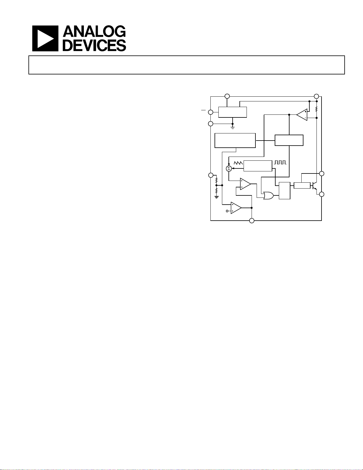
FUNCTIONAL BLOCK DIAGRAM
SD
GND
6
7
AND CURRENT LIMIT
4
FB
BIAS
3
2.50V
REGULATOR
FREQUENCY
FOLDBACK
+
1.2V
g
m
200kHz
OSCILLATOR
CMP
5
COMP
Figure 1.
CURRENT SENSE
AMPLIFIER
CURRENT
LIMIT
SQ
R
ADP3050
DRIVER
IN
8
BOOST
2
1
SWITCH
00125-001
GENERAL DESCRIPTION
The ADP3050 is a current mode monolithic buck (step down)
PWM switching regulator that contains a high current 1 A power
switch and all control, logic, and protection functions. It uses a
unique compensation scheme allowing the use of any type of
output capacitor (tantalum, ceramic, electrolytic, OS-CON).
Unlike some buck regulators, the design is not restricted to using
a specific type of output capacitor or ESR value.
A special boosted drive stage is used to saturate the NPN power
switch, providing a system efficiency higher than conventional
bipolar buck switchers. Further efficiency improvements are
obtained by using the low voltage regulated output to provide
the internal operating current of the device. A high switching
frequency allows the use of small external surface-mount components. A wide variety of standard off-the-shelf devices can be
used, providing a great deal of design flexibility. A complete
regulator design requires only a few external components.
Rev. B
Information furnished by Analog Devices is believed to be accurate and reliable. However, no
responsibility is assumed by Analog Devices for its use, nor for any infringements of patents or other
rights of third parties that may result from its use. Specifications subject to change without notice. No
license is granted by implication or otherwise under any patent or patent rights of Analog Devices.
Trademarks and registered trademarks are the property of their respective owners.
The ADP3050 includes a shutdown input that places the device
in a low power mode, reducing the total supply current to under
20 µA. Internal protection features include thermal shutdown
circuitry and a cycle-by-cycle current limit for the power switch
to provide complete device protection under fault conditions.
The ADP3050 provides excellent line and load regulation,
maintaining typically less than ±3% output voltage accuracy
over temperature and under all input voltage and output
current conditions.
The ADP3050 is specified over the industrial temperature range
of −40°C to +85°C and is available in a thermally enhanced 8-lead
(not Pb-free only) SOIC package and a standard 8-lead (Pb-free
only) RoHS-compliant SOIC package.
One Technology Way, P.O. Box 9106, Norwood, MA 02062-9106, U.S.A.
Tel: 781.329.4700 www.analog.com
Fax: 781.461.3113 ©2008 Analog Devices, Inc. All rights reserved.

ADP3050
TABLE OF CONTENTS
Features .............................................................................................. 1
Applications ....................................................................................... 1
Functional Block Diagram .............................................................. 1
General Description ......................................................................... 1
Revision History ............................................................................... 2
Specifications ..................................................................................... 3
Absolute Maximum Ratings ............................................................ 4
ESD Caution .................................................................................. 4
Pin Configuration and Function Descriptions ............................. 5
Typical Performance Characteristics ............................................. 6
Theory of Operation ...................................................................... 10
Setting the Output Voltage ........................................................ 10
Applications Information .............................................................. 11
Inductor Selection ...................................................................... 11
Output Capacitor Selection ....................................................... 12
Catch Diode Selection ............................................................... 14
Input Capacitor Selection .......................................................... 14
Discontinous Mode Ringing ..................................................... 15
Setting the Output Voltage ........................................................ 15
Frequency Compensation ......................................................... 15
Current Limit/Frequency Foldback ......................................... 16
Bias Pin Connection .................................................................. 16
Boosted Drive Stage ................................................................... 16
Start-Up/Minimum Input Voltage ........................................... 16
Thermal Considerations ............................................................ 16
Board Layout Guidelines ............................................................... 18
Typical Applications ................................................................... 18
Inverting (Buck Boost) Regulator ............................................ 19
Outline Dimensions ....................................................................... 21
Ordering Guide .......................................................................... 21
REVISION HISTORY
3/08—Rev. A to Rev. B
Updated Format .................................................................. Universal
Changes to General Description Section ...................................... 1
Changes to Figure 3 and Figure 5 ................................................... 6
Changes to Table 2 ............................................................................ 4
Deleted Table 4 ................................................................................ 14
Changes to Table 5 .......................................................................... 15
Deleted Table 8 ................................................................................ 15
Deleted Table 7 ................................................................................ 16
Deleted Table 9 ................................................................................ 16
Changes to Boosted Drive Stage Section and Thermal
Considerations Sections ............................................................ 19
Changes to Figure 27 ...................................................................... 20
Changes to Ordering Guide .......................................................... 23
Rev. B | Page 2 of 24

ADP3050
SPECIFICATIONS
VIN = 10 V, TA = −40°C to +85°C, unless otherwise noted.
Table 1.
Parameter1 Symbol Conditions Min Typ Max Unit
FEEDBACK
Feedback Voltage VFB Over line and temperature
ADP3050 1.16 1.20 1.24 V
ADP3050-3.3 3.20 3.30 3.40 V
ADP3050-5 4.85 5.00 5.15 V
Line Regulation VIN = 10 V to 30 V, no load 0.005 %/V
Load Regulation I
ADP3050AR-3.3, ADP3050AR-5 −0.5 +0.1 +0.5 %/A
Input Bias Current IFB ADP3050AR only 0.65 2 μA
ERROR AMPLIFIER
Transconductance
Voltage Gain
2
2
A
gm 1250 μMho
300 V/V
VOL
Output Current
ADP3050 COMP = 1.0 V, FB = 1.1 V to 1.3 V ±115 μA
ADP3050-3.3 COMP = 1.0 V, FB = 3.0 V to 3.6 V ±120 μA
ADP3050-5 COMP = 1.0 V, FB = 4.5 V to 5.5 V ±135 μA
OSCILLATOR
Oscillator Frequency3 f
Minimum Duty Cycle D
Maximum Duty Cycle D
170 200 240 kHz
OSC
10 %
MIN
90 %
MAX
SWITCH
Average Output Current Limit
4
I
CL(AVG)
ADP3050 BOOST = 15 V, FB = 1.1 V 1.0 1.25 1.5 A
ADP3050-3.3 BOOST = 15 V, FB = 3.0 V 1.0 1.25 1.5 A
ADP3050-5 BOOST = 15 V, FB = 4.5 V 1.0 1.25 1.5 A
Peak Switch Current Limit5 I
1.5 1.7 2.1 A
CL(PEAK)
Saturation Voltage BOOST = 15 V, I
Leakage Current 50 nA
SHUTDOWN
Input Voltage Low 0.4 V
Input Voltage High 2.0 V
SUPPLY
Input Voltage Range
Minimum BIAS Voltage V
Minimum BOOST Voltage V
6
VIN 3.6 30 V
3.0 V
BIAS
3.0 V
BOOST
IN Supply Current IQ
Normal Mode BIAS = 5.0 V 0.7 1.5 mA
Shutdown Mode
BIAS Supply Current I
BOOST Supply Current I
BIAS = 5.0 V 4.0 6.0 mA
BIAS
BOOST = 15 V, ISW = 0.5 A 18 mA
BOOST
BOOST = 15 V, ISW = 1.0 A 20 40 mA
1
All limits at temperature extremes are guaranteed via correlation using standard statistical quality control (SQC).
2
Transconductance and voltage gain measurements refer to the internal amplifier without the voltage divider. To calculate the transconductance and gain of the fixed
voltage parts, divide the values shown by FB/1.20.
3
The switching frequency is reduced when the feedback pin is lower than 0.8 × FB.
4
See Figure 24 for typical application circuit.
5
Switch current limit is measured with no diode, no inductor, and no output capacitor.
6
Minimum input voltage is not measured directly, but is guaranteed by other tests. The actual minimum input voltage needed to keep the output in regulation
depends on output voltage and load current.
= 100 mA to 1 A, ADP3050AR only −1.0 +0.1 +1.0 %/A
LOAD
= 1 A 0.65 0.95 V
LOAD
= 0 V, VIN ≤ 30 V
SD
15 40 μA
Rev. B | Page 3 of 24
ADP3050
ABSOLUTE MAXIMUM RATINGS
Table 2.
Parameter Rating
IN Voltage
Continuous −0.3 V to +40 V
Peak (<100 ms) −0.3 V to +60 V
BOOST Voltage
Continuous −0.3 V to +45 V
Peak (<100 ms) −0.3 V to +65 V
SD, BIAS Voltage
FB Voltage −0.3 V to +8 V
COMP Voltage −0.3 V to IN + 0.3 V
SWITCH Voltage −0.3 V to IN + 0.3 V
Operating Ambient Temperature Range −40°C to +85°C
Operating Junction Temperature Range −40°C to +125°C
Storage Temperature Range −65°C to +150°C
θJA (4-Layer PCB)1 60.6°C/W
θJA (4-Layer PCB)2 87.5°C/W
Lead Temperature (Soldering, 60 sec) 300°C
1
Applied to all models that are not Pb-free.
2
Applied to all Pb-free models.
−0.3 V to IN + 0.3 V
Stresses above those listed under Absolute Maximum Ratings
may cause permanent damage to the device. This is a stress
rating only; functional operation of the device at these or any
other conditions above those indicated in the operational
section of this specification is not implied. Exposure to absolute
maximum rating conditions for extended periods may affect
device reliability.
ESD CAUTION
Rev. B | Page 4 of 24
ADP3050
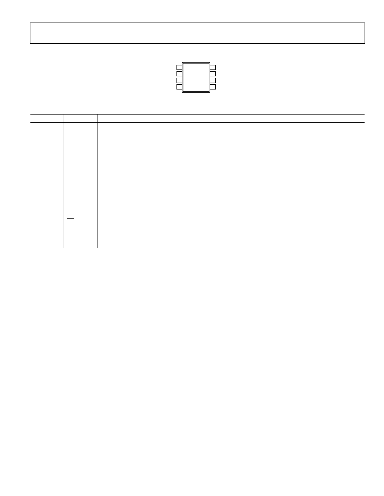
PIN CONFIGURATION AND FUNCTION DESCRIPTIONS
SWITCH
1
FB
ADP3050
2
3
TOP VIEW
(Not to Scale)
4
BOOST
BIAS
Figure 2. Pin Configuration
Table 3. Pin Function Descriptions
Pin No. Mnemonic Description
1 SWITCH
2 BOOST
Switch Node. This pin is the emitter of the internal NPN power switch. The voltage at this pin switches between
and approximately −0.5 V.
V
IN
Boost Pin. This pin is used to provide a boosted voltage (higher than V
switch. With the higher drive voltage, the power switch can be saturated, greatly reducing the switch power
losses.
3 BIAS
Bias Input Pin. Connect this pin to the regulated output voltage to maximize system efficiency. When this pin is
above 2.7 V, most of the ADP3050 operating current is taken from the output instead of the input supply. Leave
unconnected if not used.
4 FB
Feedback Pin. This feedback pin senses the regulated output voltage. Connect this pin directly to the output
(fixed output versions).
5 COMP
Compensation Node. This pin is used to compensate the regulator with an external resistor and capacitor. This
pin is also used to override the control loop. However, the voltage on this pin should not exceed 2 V, because
the pin is internally clamped to ensure a fast transient response. Use a pull-up resistor if this pin is to be pulled
higher than 2 V.
6
SD
Shutdown Pin. Use this pin to turn the device on and off. If this feature is not needed, tie this pin directly to IN.
7 GND Ground Pin. Connect this pin to local ground plane.
8 IN
Power Input. Connect this pin to the input supply voltage. An input bypass capacitor must be placed close to
this pin to ensure proper regulator operation.
8
7
6
5
IN
GND
SD
COMP
00125-002
) for the drive stage of the NPN power
IN
Rev. B | Page 5 of 24
ADP3050
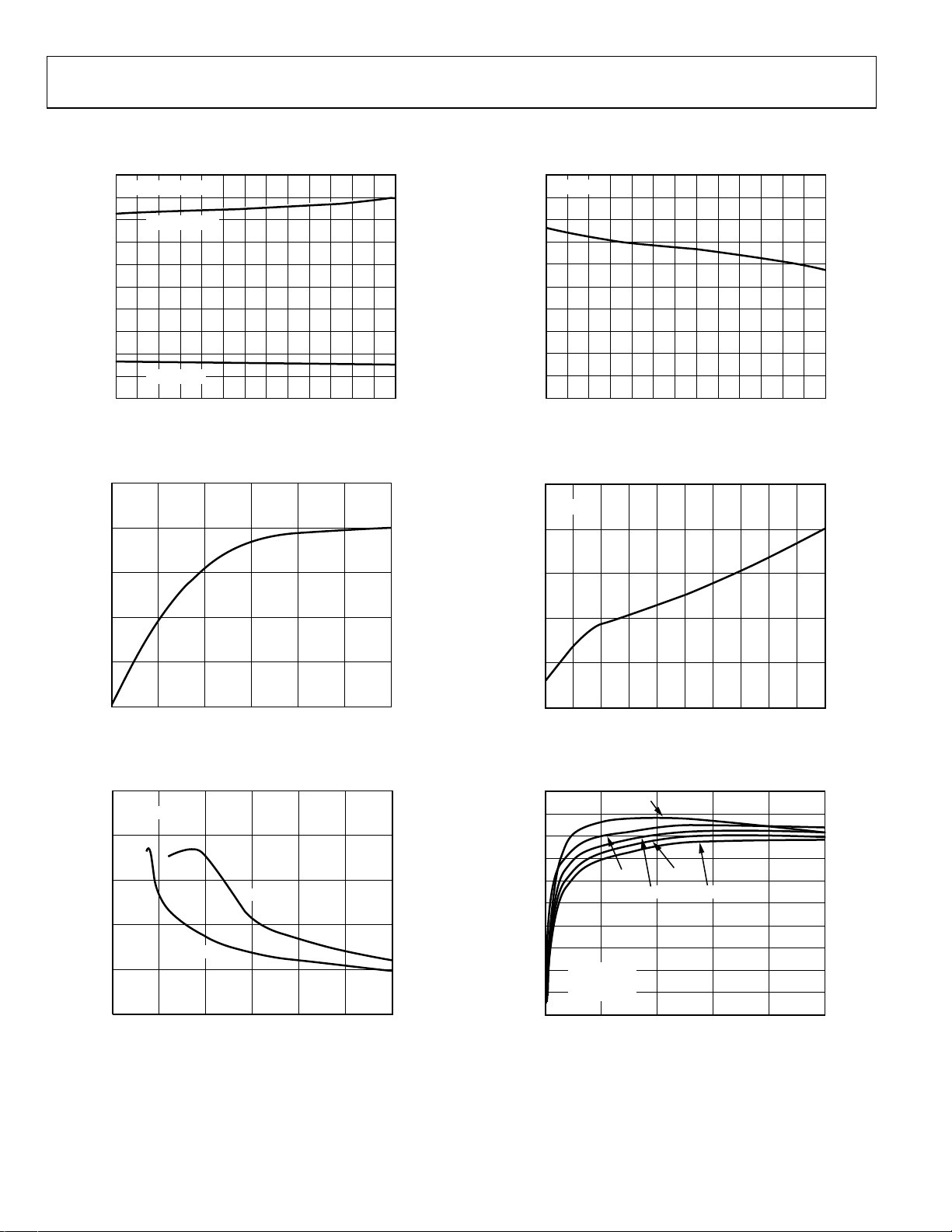
TYPICAL PERFORMANCE CHARACTERISTICS
5.0
VIN = 10V, NO L OAD
4.5
4.0
3.5
3.0
2.5
2.0
1.5
1.0
QUIESCENT O PERATING CURRENT (mA)
0.5
INTO BIAS PIN
INTO IN PIN
0
–45 –35
–25 –15 –5 5 15 25 35 45 55 65 75 85
TEMPERATURE ( °C)
Figure 3. Quiescent Operating Current vs. Temperature
25
20
15
10
2.0
VIN = 10V
1.8
1.6
1.4
1.2
1.0
0.8
0.6
0.4
AVERAGE OUTP UT CURRENT (A)
0.2
0
00125-003
–45 –35 –25 –15 –5 5 15 25 35 45 55 65 75 85
TEMPERATURE (° C)
00125-006
Figure 6. Average Output Current Limit vs. Temperature
25
VIN = 10V
20
15
10
5
SHUTDOWN QUI ESCENT CURRENT (µA)
0
5 10152025
SUPPLY VOLTAGE (V)
Figure 4. Shutdown Quiescent Current vs. Supply Voltage
10
BIAS TIED T O V
8
6
4
2
QUIESCENT O PERATING CURRENT (mA)
0
OUT
V
= 3.3V
OUT
SUPPLY VOLTAGE (V)
V
= 5V
OUT
Figure 5. Quiescent Operating Current vs. Supply Voltage
BOOST CURRENT (mA)
5
300
00125-004
0
0
0.1 0.2
0.3 0.4 0.5 0.6 0.7 0.8 0.9 1.0
LOAD CURRENT (A)
00125-007
Figure 7. Boost Current vs. Load Current
100
90
80
70
60
50
40
EFFICIE NCY (%)
30
20
10
300 5 10 15 20 25
00125-005
0
0 200 400 600 800
L = 33µH
C
= 22µF
IN
C
= 100µF
OUT
VIN = 6V
VIN = 24V
= 12V
V
IN
V
= 18V
IN
OUTPUT CURRENT (mA)
VIN = 30V
k1
00125-008
Figure 8. 5 V Output Efficiency
Rev. B | Page 6 of 24

ADP3050
100
90
80
70
60
50
40
EFFICIENCY (%)
30
20
10
0
VIN = 12V
L = 33µH
C
= 22µF
IN
= 100µF
C
OUT
V
= 5V
IN
VIN = 24V
VIN = 18V
OUTPUT CURRENT (mA)
V
= 30V
N
Figure 9. 3.3 V Output Efficiency
0.5
VIN = 10V
0.4
I
= 1A
LOAD
0.3
0.2
0.1
0
–0.1
–0.2
–0.3
OUTPUT VO LTAGE CHANGE (%)
–0.4
–0.5
–45 –35 –25 –15 –5 5 15 25 35 45 55 65 75 85
TEMPERATURE ( °C)
Figure 10. Output Voltage Change vs. Temperature
0.6
V
= 5V
OUT
0.4
0.2
= 1A
I
0
0.2
OUTPUT VO LTAGE CHANGE (%)
0.4
0.6
0
LOAD
= 100mA
I
LOAD
10 20 30
INPUT VOLTAGE (V)
Figure 11. 5 V Output Voltage Change vs. Input Voltage
0.6
V
= 3.3V
OUT
0.4
0.2
I
= 100mA
0
0.2
OUTPUT VO LTAGE CHANGE (%)
0.4
1k0 200 400 600 800
00125-009
0.6
0
LOAD
= 1A
I
LOAD
10 20 30
INPUT VOLTAGE (V)
00125-012
Figure 12. 3.3 V Output Voltage Change vs. Input Voltage
8
7
V
= 5V
6
5
4
MINIMUM INPUT VOLTAGE (V)
3
2
0
00125-010
0.1 0.2 0.3 0.4 0.5 0.6 0.7 0.8 0.9 1. 0
OUT
V
= 3.3V
OUT
LOAD CURRENT (A)
00125-013
Figure 13. Minimum Input Voltage vs. Load Current
0
–0.02
–0.04
–0.06
–0.08
–0.10
–0.12
–0.14
OUTPUT VO LTAGE CHANGE (%)
–0.16
–0.18
00125-011
VIN = 10V
0
0.10.20.30.40.50.60.70.80.91.0
LOAD CURRENT(A)
0125-014
Figure 14. Load Regulation
Rev. B | Page 7 of 24
ADP3050
A
A
0.8
0.7
0.6
VIN = 10V
VSW = 5V/DIV
0.5
0.4
0.3
0.2
SWITCH SATURATION VOLTAGE (V)
0.1
0
0.1 0.2 0.3 0.4 0.5 0.6 0.7 0.8 0.9 1.0
LOAD CURRENT (A)
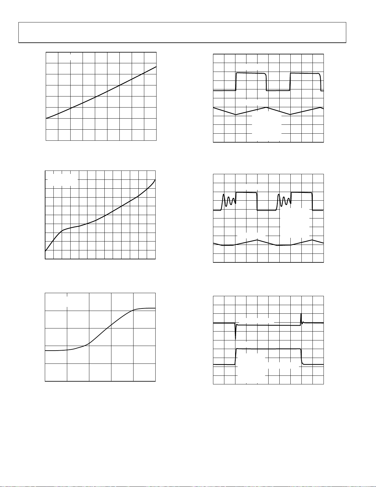
Figure 15. Switch Saturation Voltage vs. Load Current
210
VIN = 10V
208
I
= 250µA
LOAD
206
204
202
200
198
196
194
SWITCHING FREQUENCY (kHz)
192
190
–45 –35 –25 –15 –5 5 15 25 35 45 55 65 75 85
AMBIENT TEM PERATURE (°C)
Figure 16. Switching Frequency vs. Temperature
0V
= 500mA/DIV
I
L
VIN = 10V
V
= 5V
OUT
I
= 800mA
0
00125-015
LOAD
L = 33µH
C
= 22µF
IN
C
= 100µF
OUT
TIME (1µs/DIV)
00125-018
Figure 18. Continuous Conduction Mode Waveforms
VSW = 5V/DIV
0V
I
= 500mA/DIV
L
VIN = 10V
= 5V
V
OUT
= 100mA
I
LOAD
L = 33µH
= 22µF
C
IN
= 100µF
C
OUT
0
0125-016
TIME (1µs/DIV)
00125-019
Figure 19. Discontinuous Conduction Mode Waveforms
250
200
150
100
SWITCHING FREQUENCY (kHz)
50
0
0
VIN = 10V
COMP = 0.4V
NORMALIZE D FEEDBACK VOLTAGE (V)
Figure 17. Frequency Foldback
1.00.2 0.4 0.6 0.8
00125-017
Rev. B | Page 8 of 24
V
= 200mV/DIV
5V
1A
0A
OUT
I
LOAD
VIN = 10V
= 5V
V
OUT
= 100mA TO 1A SW ITCHED
I
LOAD
L = 33µH
= 22µF
C
IN
= 100µF
C
OUT
TIME (400µ s/DIV)
00125-020
Figure 20. Transient Response
 Loading...