Analog Devices ADP3050 Datasheet

200 kHz, 1 A High-Voltage
a
FEATURES
Wide Input Voltage Range: 3.6 V to 30 V
Adjustable and Fixed (3.3 V, 5 V) Output Options
Integrated 1 A Power Switch
Uses Small Surface-Mount Components
Cycle-By-Cycle Current Limiting
Peak Input Voltage (100 ms): 60 V
Thermally Enhanced 8-Lead SOIC Package
Configurable as a Buck, Buck-Boost and SEPIC
Regulator
APPLICATIONS
Industrial Power Systems
PC Peripheral Power Systems
Preregulator for Linear Regulators
Distributed Power Systems
Automotive Systems
Battery Chargers
Step-Down Switching Regulator
ADP3050
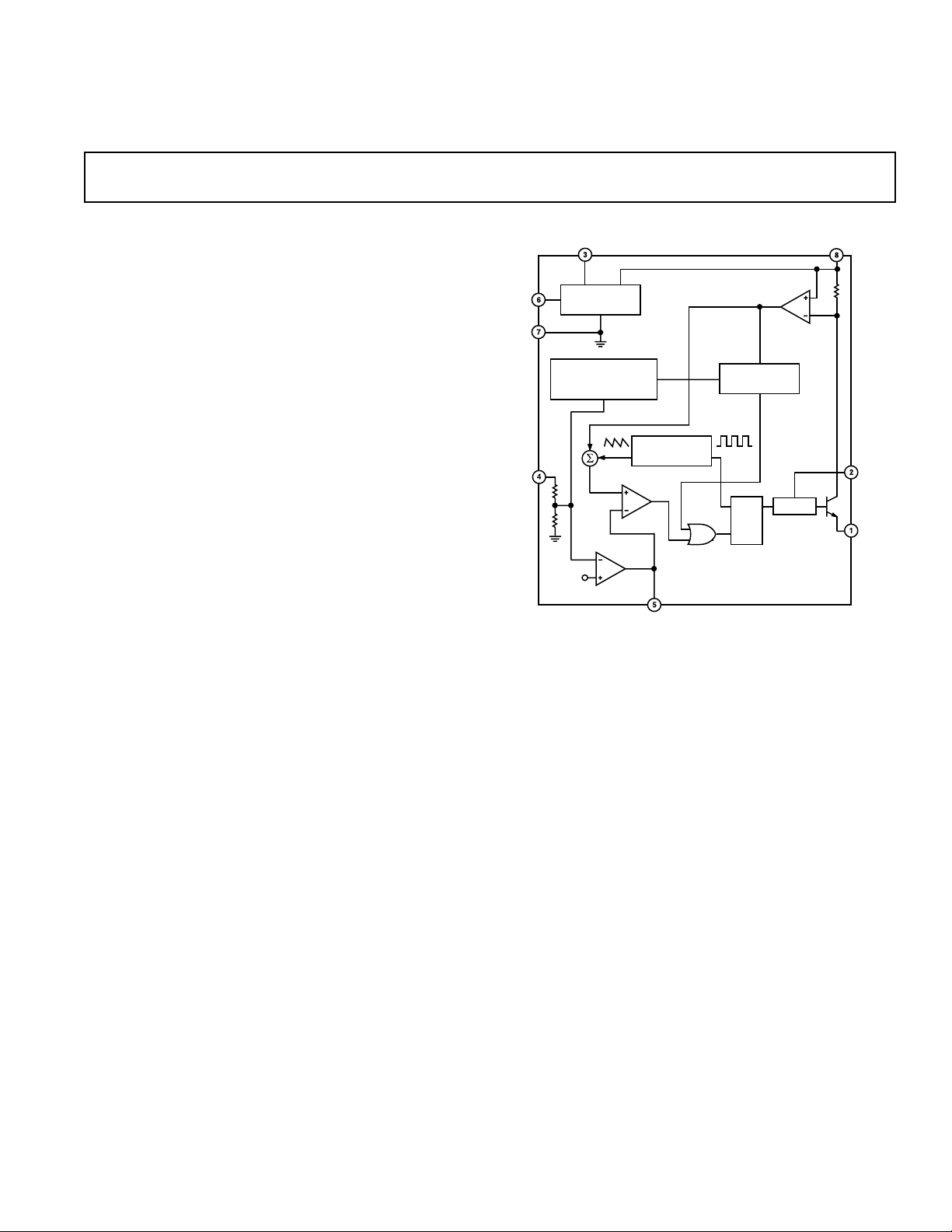
FUNCTIONAL BLOCK DIAGRAM
GND
SD
FB
BIAS
2.5V
REGULATOR
FREQUENCY
AND CURRENT LIMIT
FOLDBACK
+
g
1.2V
m
200kHz
OSCILLATOR
CMP
CURRENT SENSE
AMPLIFIER
CURRENT
LIMIT
SQ DRIVER
R
ADP3050
IN
BOOST
SWITCH
GENERAL DESCRIPTION
The ADP3050 is a current-mode monolithic buck (step-down)
PWM switching regulator that contains a high current 1 A power
switch and all control, logic, and protection functions. It uses a
unique compensation scheme that allows the use of any type of
output capacitor (tantalum, ceramic, electrolytic, OS-CON).
Unlike some buck regulators, the design is not restricted to using
a specific type of output capacitor or ESR value.
A special boosted drive stage is used to saturate the NPN power
switch, providing a system efficiency higher than conventional
bipolar buck switchers. Further efficiency improvements are obtained by using the low voltage regulated output to provide the
device's internal operating current. A high switching frequency
allows the use of small external surface-mount components. A
wide variety of standard off-the-shelf devices can be used, providing a great deal of design flexibility. A complete regulator
design requires only a few external components.
COMP
The ADP3050 includes a shutdown input that places the device
in a low-power mode, reducing the total supply current to under
20 µA. Internal protection features include thermal shutdown
circuitry and a cycle-by-cycle current-limit for the power switch
to provide complete device protection under fault conditions.
The ADP3050 provides excellent line and load regulation,
maintaining typically less than ±3% output voltage accuracy
over temperature and under all input voltage and output current
conditions.
The ADP3050 is specified over the industrial temperature range of
–40°C to +85°C and is available in a thermally enhanced 8-lead
SOIC package.
REV. 0
Information furnished by Analog Devices is believed to be accurate and
reliable. However, no responsibility is assumed by Analog Devices for its
use, nor for any infringements of patents or other rights of third parties
which may result from its use. No license is granted by implication or
otherwise under any patent or patent rights of Analog Devices.
One Technology Way, P.O. Box 9106, Norwood, MA 02062-9106, U.S.A.
Tel: 781/329-4700 World Wide Web Site: http://www.analog.com
Fax: 781/326-8703 © Analog Devices, Inc., 2000

1
ADP3050–SPECIFICATIONS
Parameter Symbol Conditions Min Typ Max Unit
FEEDBACK
Feedback Voltage V
ADP3050 1.16 1.20 1.24 V
ADP3050-3.3 3.20 3.30 3.40 V
ADP3050-5 4.85 5.00 5.15 V
Line Regulation V
Load Regulation I
Input Bias Current I
ERROR AMPLIFIER
Transconductance
Voltage Gain
2
2
Output Current
ADP3050 COMP = 1.0 V, FB = 1.1 V to 1.3 V ±115 µA
ADP3050-3.3 COMP = 1.0 V, FB = 3.0 V to 3.6 V ±120 µA
ADP3050-5 COMP = 1.0 V, FB = 4.5 V to 5.5 V ±135 µA
OSCILLATOR
Oscillator Frequency
3
Minimum Duty Cycle D
Maximum Duty Cycle D
SWITCH
Average Output Current Limit4I
ADP3050 BOOST = 15 V, FB = 1.1 V 1.0 1.25 1.5 A
ADP3050-3.3 BOOST = 15 V, FB = 3.0 V 1.0 1.25 1.5 A
ADP3050-5 BOOST = 15 V, FB = 4.5 V 1.0 1.25 1.5 A
Peak Switch Current Limit
5
Saturation Voltage BOOST = 15 V, I
Leakage Current 50 nA
SHUTDOWN
Input Voltage Low 0.4 V
Input Voltage High 2.0 V
SUPPLY
Minimum Input Voltage
6
Minimum BIAS Voltage V
Minimum BOOST Voltage V
IN Supply Current I
Normal Mode BIAS = 5.0 V 0.7 1.5 mA
Shutdown Mode SD = 0 V, V
BIAS Supply Current I
BOOST Supply Current I
NOTES
1
All limits at temperature extremes are guaranteed via correlation using standard Statistical Quality Control (SQC).
2
Transconductance and voltage gain measurements refer to the internal amplifier without the voltage divider. To calculate the transconductance and gain of the fixed
voltage parts, divide the values shown by FB/1.20.
3
The switching frequency is reduced when the feedback pin is lower than 0.8 ⫻ FB.
4
See Figure 22 for test circuit.
5
Switch current limit is measured with no diode, no inductor, and no output capacitor.
6
Minimum input voltage is not measured directly, but is guaranteed by other tests. The actual minimum input voltage needed to keep the output in regulation will
depend on output voltage and load current.
Specifications subject to change without notice.
FB
FB
g
m
A
VOL
f
OSC
MIN
MAX
CL(AVG)
I
CL(PEAK)
V
IN
BIAS
BOOST
Q
BIAS
BOOST
(VIN = 10 V, TA = –40ⴗC to +85ⴗC, unless otherwise noted)
Over Line and Temperature
= 10 V to 30 V, no load 0.005 %/V
IN
= 100 mA to 1 A,
LOAD
ADP3050AR Only –1.0 +0.1 +1.0 %/A
ADP3050AR-3.3, ADP3050AR-5 –0.5 +0.1 +0.5 %/A
ADP3050AR Only 0.65 2 µA
1250 µMho
300 V/V
170 200 240 kHz
10 %
90 %
1.5 1.7 2.1 A
= 1 A 0.65 0.95 V
LOAD
3.6 V
3.0 V
3.0 V
≤ 30 V 15 40 µA
IN
BIAS = 5.0 V 4.0 6.0 mA
BOOST = 15 V, ISW = 0.5 A 18 mA
BOOST = 15 V, ISW = 1.0 A 20 40 mA
–2–
REV. 0

ADP3050
ABSOLUTE MAXIMUM RATINGS*
IN Voltage
Steady State . . . . . . . . . . . . . . . . . . . . . . . . –0.3 V to +30 V
Peak (<100 ms) . . . . . . . . . . . . . . . . . . . . . –0.3 V to +60 V
BOOST Voltage
Steady State . . . . . . . . . . . . . . . . . . . . . . . . –0.3 V to +45 V
Peak (<100 ms) . . . . . . . . . . . . . . . . . . . . . –0.3 V to +65 V
SD, BIAS Voltage . . . . . . . . . . . . . . . . . –0.3 V to IN + 0.3 V
FB Voltage . . . . . . . . . . . . . . . . . . . . . . . . . . . . –0.3 V to +8 V
COMP Voltage . . . . . . . . . . . . . . . . . . . –0.3 V to IN + 0.3 V
SWITCH Voltage . . . . . . . . . . . . . . . . . –0.3 V to IN + 0.3 V
Operating Ambient Temperature Range . . . . –40°C to +85°C
Operating Junction Temperature Range . . . –40°C to +125°C
Storage Temperature Range . . . . . . . . . . . . –65°C to +150°C
(2-Layer PCB) . . . . . . . . . . . . . . . . . . . . . . . . . . 108°C/W
θ
JA
(4-Layer PCB) . . . . . . . . . . . . . . . . . . . . . . . . . . . 81°C/W
θ
JA
Lead Temperature Range (Soldering, 60 sec.) . . . . . . . . 300°C
*This is a stress rating only; operation beyond these limits can cause the device to
be permanently damaged. Unless otherwise specified, all voltages are referenced
to GND
ORDERING GUIDE
Output Temperature
Model Voltage Range Package*
°
ADP3050AR ADJ –40
ADP3050AR-3.3 3.3 V –40
C to +85°C SO-8
°
C to +85°C SO-8
ADP3050AR-5 5.0 V –40°C to +85°C SO-8
*SO = Small Outline Package
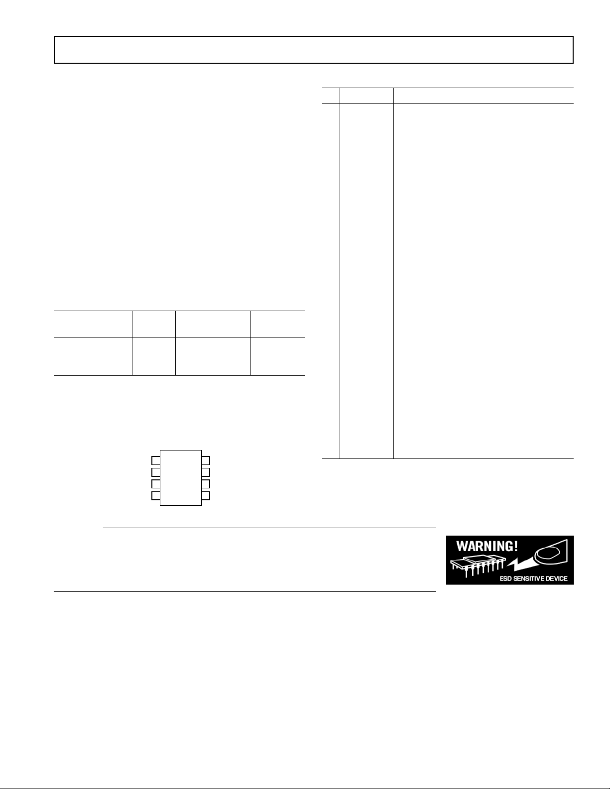
PIN CONFIGURATION
8-Lead SOIC
(R-Suffix)
SWITCH
BOOST
BIAS
FB
1
ADP3050
2
TOP VIEW
3
(Not to Scale)
4
8
7
6
5
IN
GND
SD
COMP
PIN FUNCTION DESCRIPTION
Pin Name Function
1 SWITCH This is the emitter of the internal NPN
power switch. The voltage at this pin switches
between V
and approximately –0.5 V.
IN
2 BOOST This pin is used to provide a boosted voltage
(higher than V
) for the drive stage of the
IN
NPN power switch. With the higher drive
voltage, the power switch can be saturated,
greatly reducing the switch power losses.
3 BIAS Connect this pin to the regulated output
voltage to maximize system efficiency.
When this pin is above 2.7 V, most of the
ADP3050 operating current will be taken
from the output instead of the input supply.
Leave unconnected if not used.
4 FB This feedback pin senses the regulated output
voltage. Connect this pin directly to the output (fixed output versions).
5 COMP This pin is used to compensate the regulator
with an external resistor and capacitor. This
pin can be used to override the control loop,
but the voltage on this pin should not exceed
about 2 V, as the pin is internally clamped to
ensure a fast transient response. Use a pull-up
resistor if this pin is to be pulled higher than 2 V.
6 SD Use this pin to turn the device on and off. If
this feature is not needed, tie this pin directly
.
to V
IN
7 GND Connect this pin to local ground plane.
8 IN Connect this pin to the input supply voltage.
An input bypass capacitor must be placed
close to this pin to ensure proper regulator
operation.
CAUTION
ESD (electrostatic discharge) sensitive device. Electrostatic charges as high as 4000 V readily
accumulate on the human body and test equipment and can discharge without detection.
Although this device features proprietary ESD protection circuitry, permanent damage may occur
on devices subjected to high energy electrostatic discharges. Therefore, proper ESD
precautions are recommended to avoid performance degradation or loss of functionality.
REV. 0
–3–

ADP3050
– Typical Characteristics
5.0
VIN = 10V, NO LOAD
4.5
4.0
3.5
3.0
2.5
2.0
1.5
1.0
QUIESCENT OPERATING CURRENT – mA
0.5
0
ⴚ4585ⴚ35
INTO BIAS PIN
INTO VIN PIN
ⴚ25 ⴚ15 ⴚ5
5 152535455565 75
TEMPERATURE – ⴗC
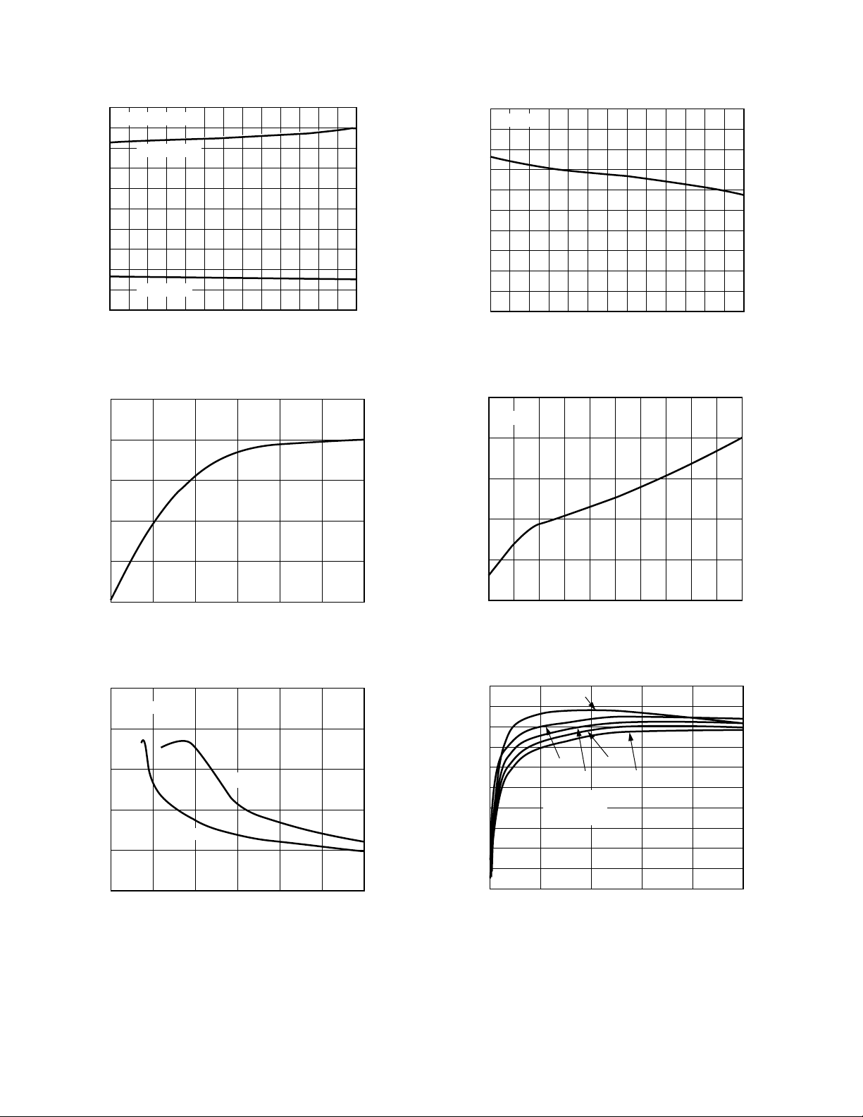
Figure 1. Quiescent Operating Current vs. Temperature
25
20
15
2.0
VIN = 10V
1.8
1.6
1.4
1.2
1.0
0.8
0.6
0.4
AVERAGE OUTPUT CURRENT – A
0.2
0
ⴚ25 ⴚ15 ⴚ5
ⴚ4585ⴚ35
5 152535455565 75
TEMPERATURE – ⴗC
Figure 4. Average Output Current Limit vs. Temperature
25
VIN = 10V
20
15
10
5
SHUTDOWN QUIESCENT CURRENT – A
0
030
10 15 20 25
5
SUPPLY VOLTAGE – V
Figure 2. Shutdown Quiescent Current vs. Supply Voltage
10
BIAS TIED TO V
8
6
4
2
QUIESCENT OPERATING CURRENT – mA
0
030
OUT
V
OUT
V
= 3.3V
OUT
10 15 20 25
5
SUPPLY VOLTAGE – V
= 5V
Figure 3. Quiescent Operating Current vs. Supply Voltage
10
BOOST CURRENT – mA
5
0
0
0.2 0.3 0.4 0.5 0.6 0.7 0.8 0.9
LOAD CURRENT – A
Figure 5. Boost Current vs. Load Current
100
90
80
70
60
50
40
EFFICIENCY – %
30
20
10
0
01k200 400 600 800
VIN = 6V
VIN = 24V
= 12V
V
IN
VIN = 18V
L = 33H
C
IN
C
OUT
VIN = 30V
= 22F
= 100F
OUTPUT CURRENT – mA
Figure 6. 5 V Output Efficiency
1.00.1
–4–
REV. 0

ADP3050
INPUT VOLTAGE – V
0
OUTPUT VOLTAGE CHANGE – %
10 20 30
0.6
0.2
0.4
0
ⴚ0.6
ⴚ0.4
ⴚ0.2
V
OUT
= 3.3V
I
LOAD
= 1A
I
LOAD
= 100mA
100
90
80
70
60
50
40
EFFICIENCY – %
30
20
10
0
01k200 400 600 800
= 5V
V
IN
VIN = 12V
VIN = 24V
VIN = 18V
L = 33H
C
= 22F
IN
= 100F
C
OUT
OUTPUT CURRENT – mA
V
IN
= 30V
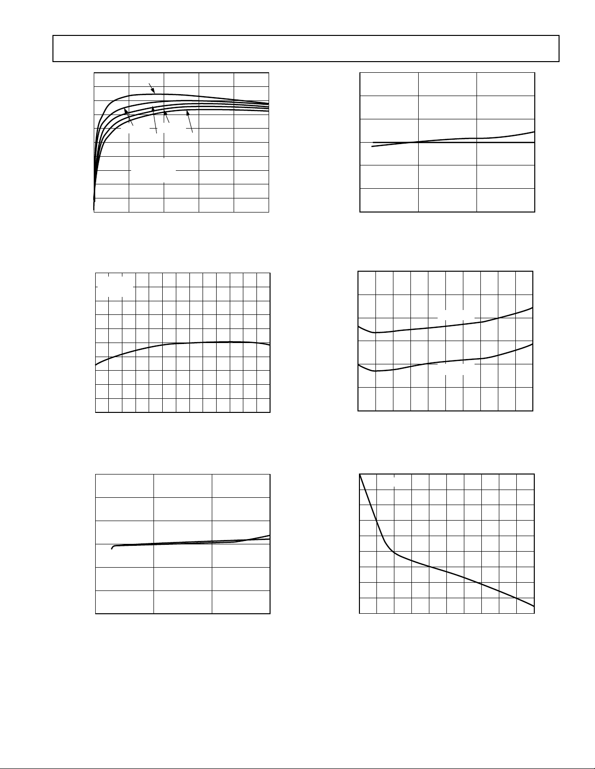
Figure 7. 3.3 V Output Efficiency
0.5
VIN = 10V
ⴚ0.1
ⴚ0.2
ⴚ0.3
OUTPUT VOLTAGE CHANGE – %
ⴚ0.4
ⴚ0.5
0.4
0.3
0.2
0.1
I
LOAD
0
ⴚ4585ⴚ35
= 1A
ⴚ25 ⴚ15 ⴚ5
5 152535455565 75
TEMPERATURE – ⴗC
Figure 8. Output Voltage Change vs. Temperature
Figure 10. 3.3 V Output Voltage Change vs. Input Voltage
8
7
V
= 5V
6
5
4
MINIMUM INPUT VOLTAGE – V
3
2
0
0.2 0.3 0.4 0.5 0.6 0.7 0.8 0.9
OUT
V
= 3.3V
OUT
LOAD CURRENT – A
1.00.1
Figure 11. Minimum Input Voltage vs. Load Current
ⴚ0.02
ⴚ0.04
ⴚ0.06
ⴚ0.08
ⴚ0.10
ⴚ0.12
ⴚ0.14
OUTPUT VOLTAGE CHANGE – %
ⴚ0.16
ⴚ0.18
0
VIN = 10V
01.00.1 0.2 0.3 0.4 0.5 0.6 0.7 0.8 0.9
LOAD CURRENT – A
Figure 12. Load Regulation
0.6
V
= 5V
OUT
0.4
0.2
I
= 1A
0.0
ⴚ0.2
OUTPUT VOLTAGE CHANGE – %
ⴚ0.4
ⴚ0.6
0
LOAD
I
= 100mA
LOAD
10
INPUT VOLTAGE – V
20 30
Figure 9. 5 V Output Voltage Change vs. Input Voltage
REV. 0
–5–
 Loading...