ANALOG DEVICES ADP3041 Service Manual

查询ADP3041供应商查询ADP3041供应商
TFT LCD Panel Power Module
ADP3041
FEATURES
600 kHz PWM Frequency
Fully Integrated 1.5 A Power Switch
3% Output Regulation Accuracy
Simple Compensation
Small Inductor and MLC Capacitors
300 A Quiescent Supply Current
90% Efficiency
Undervoltage Lockout
5 Buffers
TSSOP 20-Lead Package
Pb-Free Part
APPLICATIONS
TFT LCD Bias Supplies
GENERAL DESCRIPTION
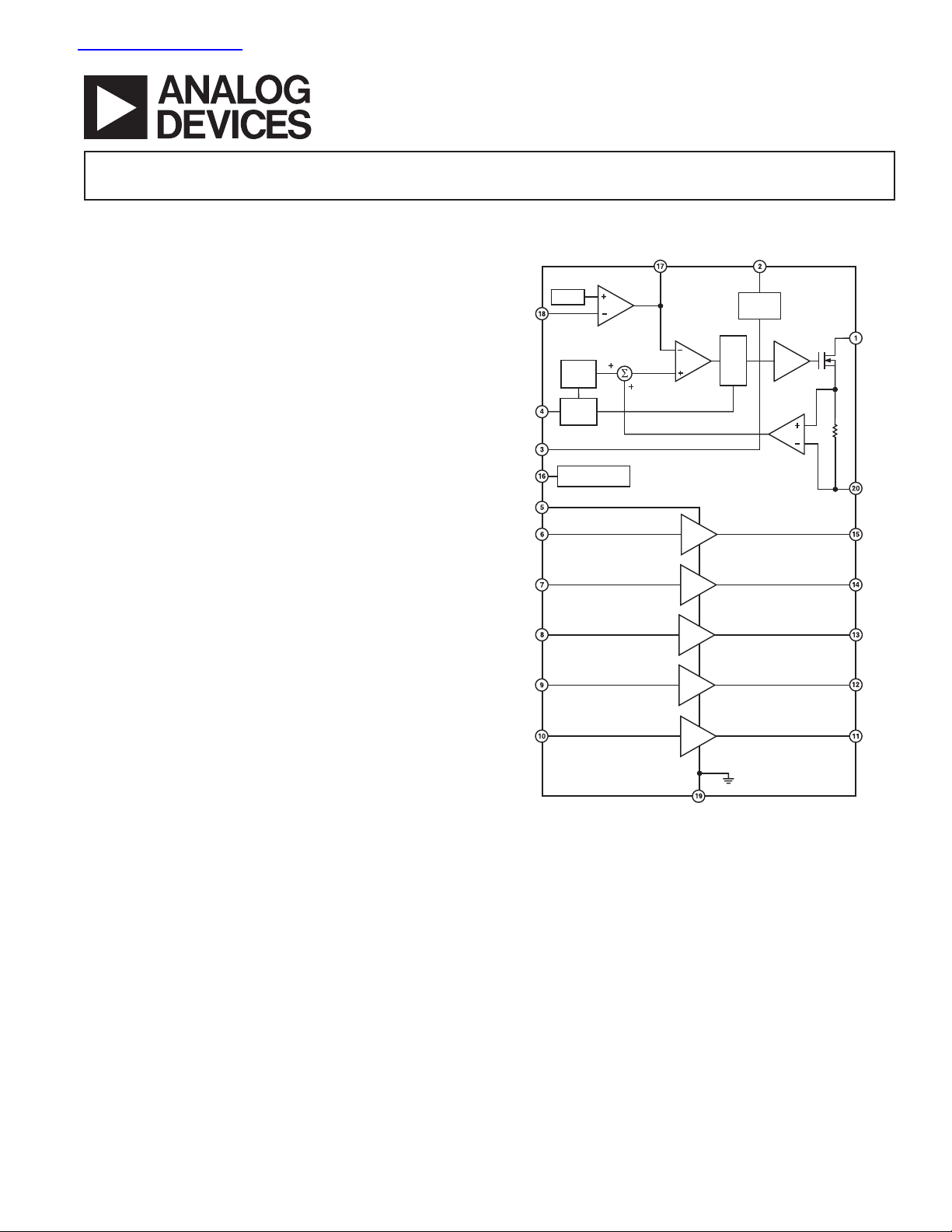
The ADP3041 is a fixed frequency, PWM step-up dc-to-dc
switching regulator with five buffers capable of 12 V boosted
output voltage in a TSSOP 20-lead package. It provides high
efficiency, low noise operation, and excellent dynamic response,
and is easy to use. The high switching frequency allows for small,
cost-saving, external inductive and capacitive components. The
ADP3041 operates in PWM current mode. The current limit
and the power switch are integrated completely on-chip.
Capable of operating from 2.5 V to 5.5 V input, the ADP3041
is ideal for thin-film transistor (TFT) liquid crystal display
(LCD) module applications, where local point-of-use power
regulation is required. Supporting output voltages down to 4.5 V,
the ADP3041 is ideal to generate today’s low voltage rails, providing the optimal solution in its class for delivering power
efficiently, responsively, and simply with minimal printed circuit
board area.
The ADP3041 integrates five buffers. Each buffer can deliver
35 mA output current and has rail-to-rail input and output
capability.
FB
NC
SD
SS
AVCC
VCMI
G1I
G2I
G3I
G4I
FUNCTIONAL BLOCK DIAGRAM
REF
RAMP
GEN
OSC
SOFT START
g
m
ERROR
AMP
COMP
COMPARATOR
AGND
IN
BIAS
F/F
R
Q
S
ADP3041
DRIVER
CURRENT
SENSE
AMPLIFIER
SW
PGND
VCMO
G1O
G2O
G3O
G4O
REV. D
Information furnished by Analog Devices is believed to be accurate and
reliable. However, no responsibility is assumed by Analog Devices for its
use, nor for any infringements of patents or other rights of third parties that
may result from its use. No license is granted by implication or otherwise
under any patent or patent rights of Analog Devices. Trademarks and
registered trademarks are the property of their respective owners.
One Technology Way, P.O. Box 9106, Norwood, MA 02062-9106, U.S.A.
Tel: 781/329-4700 www.analog.com
Fax: 781/326-8703 © 2003 Analog Devices, Inc. All rights reserved.

1
ADP3041–SPECIFICATIONS
Parameter Symbol Conditions Min Typ Max Unit
SUPPLY
Input Voltage V
Operating Current
2
Quiescent Current I
Shutdown Current I
ERROR AMPLIFIER
Feedback Voltage Accuracy V
Line Regulation V
FB Bias Current 100 nA
Overall Regulation Line, Temperature –3 +3 %
OUTPUT SWITCH
On Resistance R
Output Load Current I
Leakage Current V
Efficiency I
OSCILLATOR
Oscillator Frequency f
Maximum Duty Cycle D
Minimum Duty Cycle D
SOFT START
Charge Current VSS = 3.3 V, CSS = 1 nF 2.5 µA
SHUTDOWN
Input Voltage Low 0.8 V
Input Voltage High 2.2 V
CURRENT LIMIT
Peak Switch Current I
COMPENSATION
Transconductance g
Gain A
UNDERVOLTAGE LOCKOUT
UVLO Threshold 2.2 2.4 2.5 V
UVLO Hysteresis 130 mV
OUTPUT
Voltage Range V
Load Regulation I
IN
I
QSW
Q
SD
FB
DS (ON)
LOAD
OSC
MAX
MIN
CL
m
V
OUT
(VIN = 3.3 V, TA = –40ⴗC to +85ⴗC, unless otherwise noted.)
2.5 3.3 5.5 V
f = 600 kHz, No Load, 1 5 mA
AVCC = Open
Not Switching, AVCC = Open 270 500 µA
AVCC = Open 10 µA
1.215 1.233 1.251 V
= 2.5 V to 5.5 V –0.15 +0.15 %/V
IN
At 1.5 A, VIN = 3.3 V 300 mΩ
Continuous Operation,
= 3.3 V, V
V
IN
SWITCH
= 200 mA, V
LOAD
I
= 100 mA, V
LOAD
= 12 V, SD = 0 V 5 µA
= 10 V 300 mA
OUT
= 10 V 90 %
OUT
= 10 V 90 %
OUT
0.4 0.6 0.9 MHz
COMP = Open, FB = 1 V 80 90 %
COMP = Open, FB = 1 V 40 %
1.5 1.8 A
100 µA/V
1000 V/V
VIN = 2.5 V to 5.5 V 4.5 12 V
= 10 mA to 150 mA,
LOAD
V
= 10 V 0.05 mV/mA
OUT
REV. D–2–

ADP3041
Parameter Symbol Conditions Min Typ Max Unit
BUFFER INPUT
CHARACTERISTICS
Offset Voltage V
Offset Voltage Drift ⌬V
Input Bias Current I
OS
/⌬T –40°C ≤ TA ≤ +85°C5µV/°C
OS
B
–40°C ≤ T
≤ +85°C 800 nA
A
Input Voltage Range –0.5 V
Input Impedance Z
Input Capacitance C
IN
IN
OUTPUT CHARACTERISTICS
Output Voltage High V
Output Voltage Low V
Continuous Output Current I
Peak Output Current I
OH
OL
OUT
PK
IL = 100 µAV
V
= 12 V, IL = 5 mA 11.85 11.94 V
S
–40°C ≤ T
= 4.5 V, IL = 5 mA 4.2 4.38 V
V
S
–40°C ≤ T
≤ +85°C 11.75 V
A
≤ +85°C 4.1 V
A
IL = 100 µA5mV
= 12 V, IL = 5 mA 42 150 mV
V
S
–40°C ≤ T
V
= 4.5 V, IL = 5 mA 95 300 mV
S
≤ +85°C 250 mV
A
VS = 12 V 250 mA
TRANSFER CHARACTERISTICS
Gain AVCL R
Gain Linearity NL R
= 2 kΩ 0.995 0.9985 1.005 V/V
L
–40°C ≤ T
= 2 kΩ,
L
≤ +85°C 0.995 0.9985 1.005 V/V
A
VO = 0.5 to (VS – 0.5 V) 0.01 %
POWER SUPPLY
Supply Voltage V
S
Power Supply Rejection Ratio PSRR V
Supply Current/Amplifier I
SY
= 4 V to 12 V,
S
–40°C ≤ T
≤ +85°C7090 dB
A
VO = VS/2, No Load 780 1000 µA
4.5 12 V
–40°C ≤ TA ≤ +85°C 1.2 mA
DYNAMIC PERFORMANCE
Slew Rate SR RL = 10 kΩ, CL = 200 pF 4.5 8 V/µs
Bandwidth BW –3 dB, R
Phase Margin mR
L
= 10 kΩ, CL = 10 pF 8 MHz
L
= 10 kΩ, CL = 10 pF 65 Degrees
NOISE PERFORMANCE
Voltage Noise Density e
Current Noise Density i
NOTES
1
All limits at temperature extremes are guaranteed via correlation and characterization using standard Statistical Quality Control (SQC).
2
This is the average current while switching.
Specifications subject to change without notice.
n
e
n
n
f = 1 kHz 27 nV/√Hz
f = 10 kHz 25 nV/√Hz
f = 10 kHz 0.8 pA/√Hz
210mV
80 600 nA
+ 0.5 V
S
400 kΩ
1pF
– 0.005 V
S
400 mV
35 mA
REV. D
–3–

ADP3041
SS
COMP
SW
FB
IN
PGND
SD
VCMO
G1O
AGND
G2O
G3O
G4O
G1I
G2I
G3I
G4I
VCMI
AVCC
NC
TOP VIEW
(Not to Scale)
20
19
18
17
16
15
14
13
12
11
NC = NO CONNECT
1
2
3
4
5
6
7
8
9
10
ADP3041
ABSOLUTE MAXIMUM RATINGS*
Input Voltage . . . . . . . . . . . . . . . . . . . . . . . . . . –0.3 V to + 6 V
Buffer Input Voltage . . . . . . . . . . . . . –0.5 V to AVCC + 0.5 V
SW Voltage . . . . . . . . . . . . . . . . . . . . . . . . . . . . . . . . . . . . 14 V
COMP Voltage . . . . . . . . . . . . . . . . . . . . . . . –0.3 V to +2.5 V
FB Voltage . . . . . . . . . . . . . . . . . . . . . . . . . . . –0.3 V to +1.3 V
SD Voltage . . . . . . . . . . . . . . . . . . . . . . . . . . . . –0.3 V to +6 V
PGND to GND . . . . . . . . . . . . . . . . . . . . . . . . . . . . . ±200 mV
Operating Ambient Temperature Range . . . . .–40°C to +85°C
Operating Junction Temperature Range . . . . –40°C to +125°C
Storage Temperature Range . . . . . . . . . . . . .–65°C to +150°C
2-Layer . . . . . . . . . . . . . . . . . . . . . . . . . . . . . . . . . 143°C/W
JA
4-Layer . . . . . . . . . . . . . . . . . . . . . . . . . . . . . . . . . 112°C/W
JA
Lead Temperature Range (Soldering 60 sec) . . . . . . . . . 300°C
*Stresses above those listed under Absolute Maximum Ratings may cause perma-
nent damage to the device. This is a stress rating only; functional operation of the
device at these or any other conditions above those listed in the operational
sections of this specification is not implied. Exposure to absolute maximum ratings
for extended periods may affect device reliability.
ORDERING GUIDE
Temperature Voltage Package
Model Range Output Option
ADP3041ARU –40°C to +85°C 4.5 V to 12 V TSSOP-20
ADP3041ARUZ* –40°C to +85°C 4.5 V to 12 V TSSOP-20
*Z = Pb-free part.
D1
R1
C
OUT
L1
SW
V
IN
C
IN
R
SD
ADP3041
IN
SD
NC
AVCC
VCMI
G1I
G2I
G3I
G4I
PGND
AGND
FB
COMP
SS
VCMO
G1O
G2O
G3O
G4O
R2
C
C
R
C
C
SS
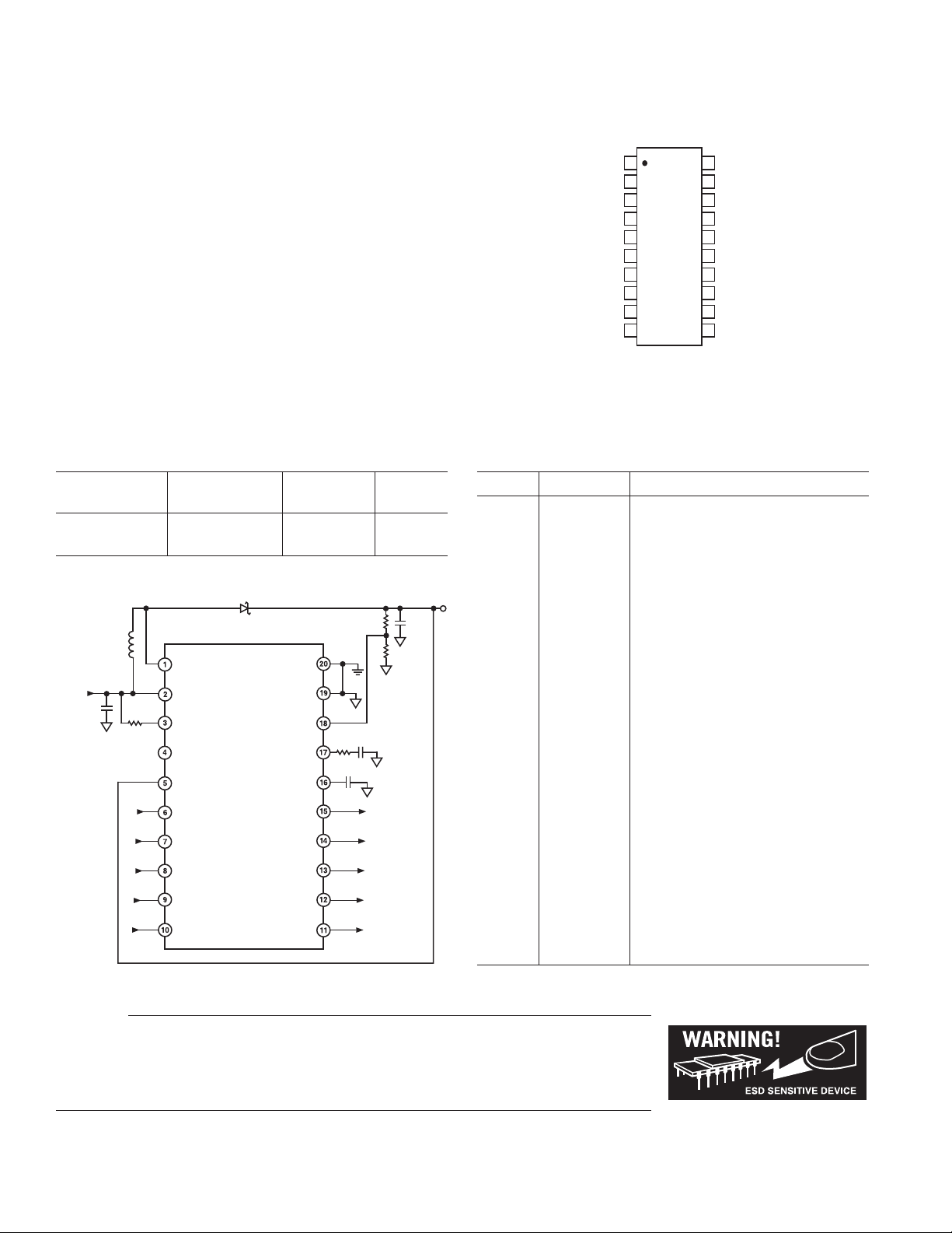
PIN CONFIGURATION
PIN FUNCTION DESCRIPTIONS
Pin No. Mnemonic Function
1SWSwitching Output
2INMain Power Supply Input
3 SD Shutdown Input
4NCNo Connection
5 AVCC Buffers Power Supply Input
6 VCMI VCOM Buffer Input
7 G1I Gamma 1 Buffer Input
8 G2I Gamma 2 Buffer Input
9 G3I Gamma 3 Buffer Input
10 G4I Gamma 4 Buffer Input
11 G4O Gamma 4 Buffer Output
12 G3O Gamma 3 Buffer Output
13 G2O Gamma 2 Buffer Output
14 G1O Gamma 1 Buffer Output
15 VCMO VCOM Buffer Output
16 SS Soft Start Capacitor Timer Set
17 COMP Compensation Input
18 FB Feedback Voltage Sense Input
19 AGND Analog Signal Ground
20 PGND Ground Return for Power Transistor
Figure 1. Typical Application
CAUTION
ESD (electrostatic discharge) sensitive device. Electrostatic charges as high as 4000 V readily
accumulate on the human body and test equipment and can discharge without detection. Although the
ADP3041 features proprietary ESD protection circuitry, permanent damage may occur on devices
subjected to high energy electrostatic discharges. Therefore, proper ESD precautions are recommended
to avoid performance degradation or loss of functionality.
REV. D–4–

Typical Performance Characteristics–
TEMPERATURE (ⴗC)
5
–5
–40
INPUT OFFSET CURRENT (nA)
25 85
–2
–3
–4
VS = 16V
VS = 4.5V
–1
4
3
2
1
0
ADP3041
100
TA = 25ⴗC
90
80
70
60
50
40
30
QUANTITY (Amplifiers)
20
10
0
–12 –9
4.5V < V
< 16V
S
–6 –3 0 3 6 9 12
INPUT OFFSET VOLTAGE (mV)
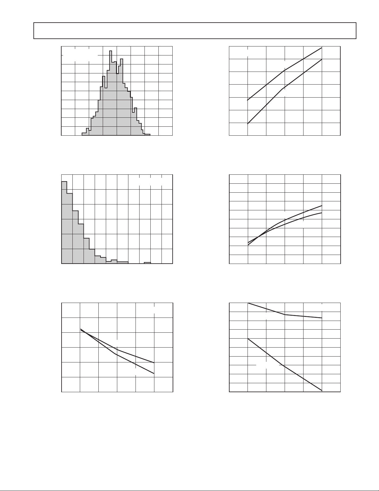
TPC 1. Input Offset Voltage Distribution
300
4.5V < VS < 16V
250
200
150
0
VCM = VS/2
–50
–100
–150
–200
–250
INPUT BIAS CURRENT (nA)
–300
–350
–40
VS = 16V
VS = 4.5V
25 85
TEMPERATURE (ⴗC)
TPC 4. Input Bias Current vs. Temperature
QUANTITY (Amplifiers)
–0.25
–0.50
–0.75
–1.00
INPUT OFFSET VOLTAGE (mV)
–1.25
–1.50
REV. D
100
50
0
0 10010
20 30 40 50 60 70 80 90
TCVOS (V/ⴗC)
TPC 2. Input Offset Voltage Drift Distribution
0
VCM = VS/2
VS = 16V
VS = 4.5V
–40
25 85
TEMPERATURE (ⴗC)
TPC 3. Input Offset Voltage vs. Temperature
–5–
TPC 5. Input Offset Current vs. Temperature
15.96
15.95
15.94
15.93
15.92
15.91
15.90
15.89
OUTPUT VOLTAGE SWING (V)
15.88
15.87
15.86
VS = 16V
VS = 4.5V
–40
25 85
TEMPERATURE (ⴗC)
I
LOAD
= 5mA
TPC 6. Output Voltage Swing vs. Temperature
4.46
4.45
4.44
4.43
4.42
4.41
4.40
4.39
4.38
4.37
4.36
 Loading...