Analog Devices ADP3026 Datasheet

High Efficiency Dual
FEATURES
Wide input voltage range: 5.5 V to 25 V
High conversion efficiency > 96%
Integrated current sense—no external resistor required
Low shutdown current: 19 µA (typical)
Voltage mode PWM with input feed-forward for fast line
transient response
Dual synchronous buck controllers
Built-in gate drive boost circuit for driving external
N-channel MOSFETs
2 fixed output voltages: 3.3 V and 5 V
PWM frequency: 200 kHz
Extensive circuit protection functions
APPLICATIONS
Portable instruments
General-purpose dc-to-dc converters
Power Supply Controller
ADP3026
GENERAL DESCRIPTION
The ADP3026 is a highly efficient dual synchronous buck
switching regulator controller optimized for converting a
battery or adapter input into multiple supply voltages. The
ADP3026 provides accurate and reliable short-circuit protection
using an internal current sense circuit, which reduces cost and
increases overall efficiency. Other protection features include
programmable soft start, UVLO, and integrated output
undervoltage/overvoltage protection.
The ADP3026 is specified over the 0°C to 70°C commercial
temperature range and is available in a 28-lead TSSOP package.
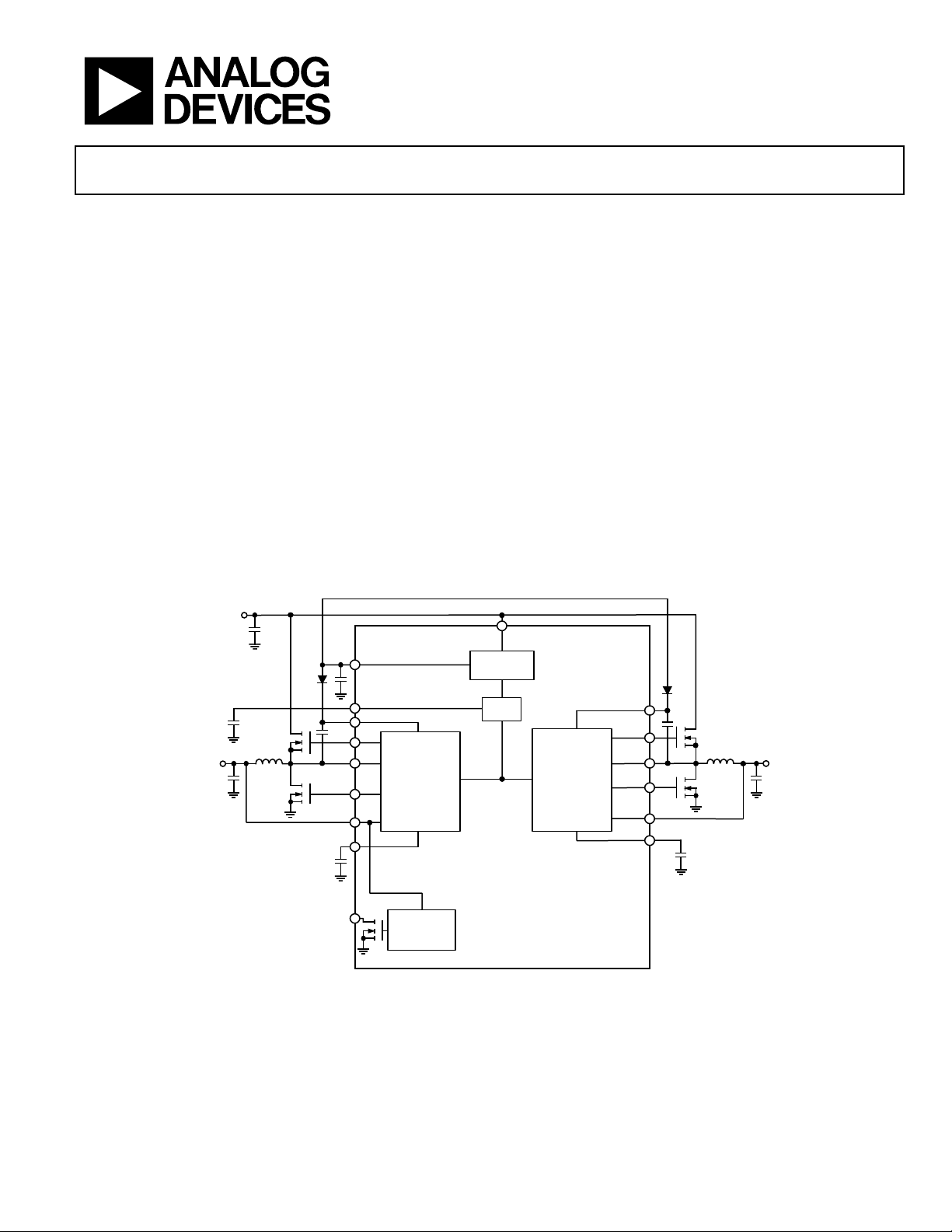
FUNCTIONAL BLOCK DIAGRAM
V
IN
5.5V TO 25V
5V LINEAR
REF
SS3
Q1
Q2
L1
3.3V
02950-001
Q3
5V
L2
Q4
SS5
PWRGD
5V
SMPS
POWER-ON
RESET
ADP3026
Figure 1.
3.3V
3.3V
SMPS
Rev. 0
Information furnished by Analog Devices is believed to be accurate and reliable.
However, no responsibility is assumed by Analog Devices for its use, nor for any
infringements of patents or other rights of third parties that may result from its use.
Specifications subject to change without notice. No license is granted by implication
or otherwise under any patent or patent rights of Analog Devices. Trademarks and
registered trademarks are the property of their respective owners.
One Technology Way, P.O. Box 9106, Norwood, MA 02062-9106, U.S.A.
Tel: 781.329.4700
Fax: 781.326.8703
www.analog.com
© 2004 Analog Devices, Inc. All rights reserved.

ADP3026
TABLE OF CONTENTS
Specifications..................................................................................... 3
Circuit Description .................................................................... 10
Absolute Maximum Ratings............................................................ 5
ESD Caution.................................................................................. 5
Pin Configuration and Function Descriptions............................. 6
Typical Performance Characteristics ............................................. 8
Theory of Operation ...................................................................... 10
REVISION HISTORY
10/04—Revision 0: Initial Version
Application Information ........................................................... 11
Layout Considerations............................................................... 16
Outline Dimensions....................................................................... 18
Ordering Guide .......................................................................... 18
Rev. 0 | Page 2 of 20

ADP3026
SPECIFICATIONS
@ TA = 0°C to 70°C, VIN = 12 V, SS5 = SS3 = INTVCC, INTVCC Load = 0 mA, REF Load = 0 mA, SD = 5 V, unless otherwise noted.
All limits at temperature extremes are guaranteed via correlation using standard Statistical Quality Control (SQC) methods.
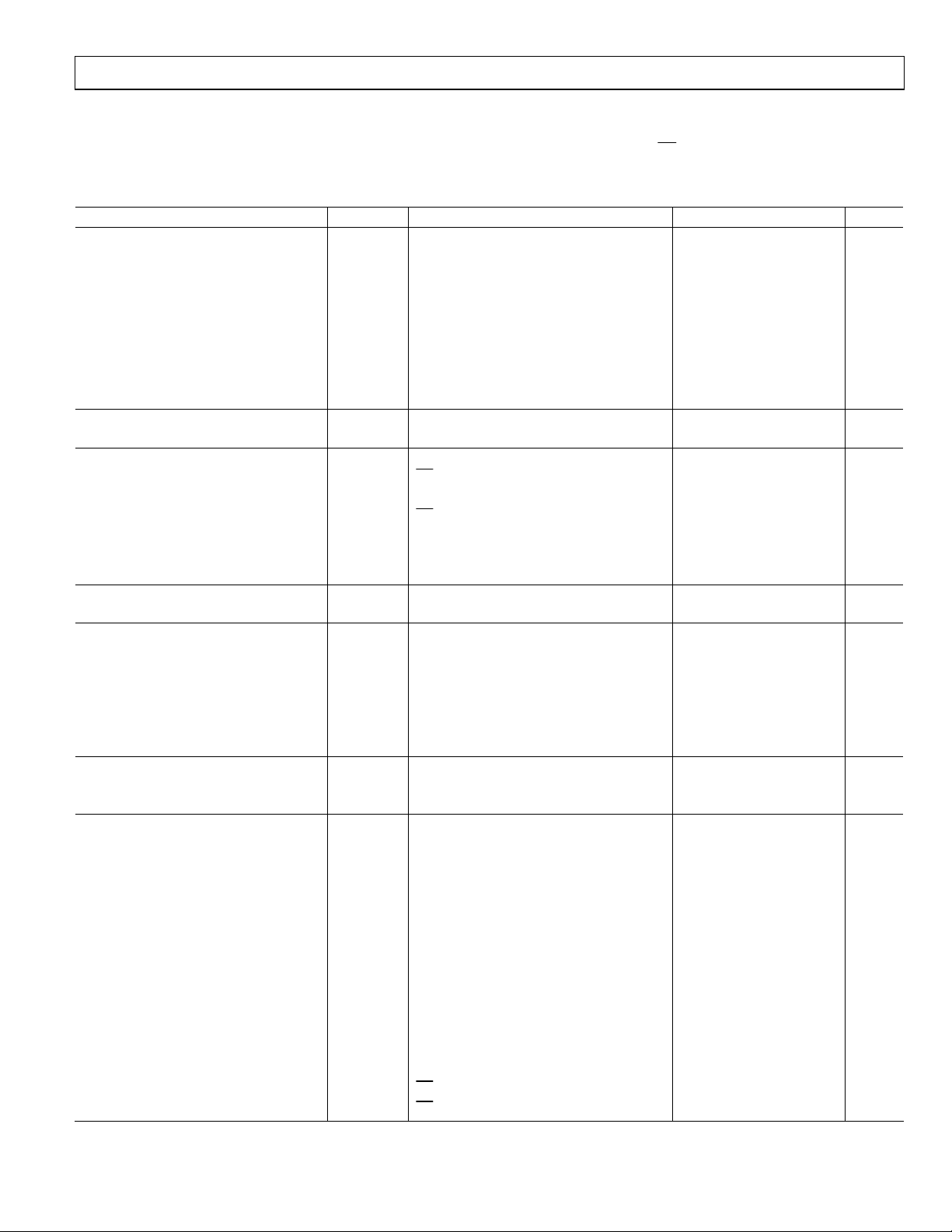
Table 1.
Parameter Symbol Conditions Min Typ Max Unit
INTERNAL 5 V REGULATOR INTVCC
Input Voltage Range 5.5 25 V
5 V Voltage TA = 25°C 4.95 5.02 5.15 V
Line Regulation 5.5 V ≤ VIN ≤ 25 V 1.0 mV/V
Total Variation Line, temperature 4.8 5.2 V
Undervoltage Lockout INTVCC falling 4.05 4.25 4.5 V
Threshold Voltage
Undervoltage Lockout 270 mV
Hysteresis
REFERENCE
Output Voltage1 REF 5.5 V ≤ VIN ≤ 25 V 784 800 816 V
SUPPLY CURRENT IQ
Shutdown Current
SD
= 0 V
Standby Current SS3 = SS5 = 0 V 120 200 µA
SD
= 5 V
Quiescent Current No loads 1.3 1.9 mA
SS3 = SS5 = 5 V
FB5 = 5.05 V, FB3 = 3.33 V
OSCILLATOR
Frequency f
5.5 V ≤ VIN ≤ 25 V 165 200 235 kHz
OSC
POWER GOOD PWRGD
Output Voltage in Regulation 10 kΩ pull-up to 5 V 4.8 V
Output Voltage out of Regulation 10 kΩ pull-up to 5 V 0.4 V
FB5 < 90% of nominal output value
PWRGD Trip Threshold FB5 rising −6 −3.7 −1.5 %
PWRGD Hysteresis FB5 falling 4 %
CPOR Pull-Up Current CPOR = 1.2 V −3 −1 −0.3 µA
ERROR AMPLIFIER
DC Gain2 47 dB
Gain-Bandwidth Product2 GBW 10 MHz
MAIN SMPS CONTROLLERS
Fixed 5 V Output Voltage FB5 5.5 V ≤ VIN ≤25 V 4.90 5.0 5.10 V
Fixed 3.3 V Output Voltage FB3 5.5 V ≤ VIN ≤25 V 3.234 3.3 3.366 V
Current Limit Threshold
CLSET5 = CLSET3 = Floating 5.5 V ≤ VIN ≤ 25 V, TA = 25°C 54 72 90 mV
CLSET5 = CLSET3 = 0 V 5.5 V ≤ VIN ≤ 25 V, TA = 25°C 240 300 360 mV
Soft-Start Current SS3 = SS5 = 3 V 0.7 2.1 3.8 µA
Soft-Start Turn-On Threshold SS5, SS3 0.4 0.6 0.8 V
Transition Time (DRVL)
Rise tR(DRVL) C
Fall tF(DRVL) C
= 3000 pF, 10% to 90% 40 70 ns
LOAD
= 3000 pF, 90% to 10% 45 70 ns
LOAD
Transition Time (DRVH)
Rise tR(DRVH) C
Fall tF(DRVH) C
Logic Input Low Voltage
Logic Input High Voltage
= 3000 pF, 10% to 90% 50 100 ns
LOAD
= 3000 pF, 90% to 10% 50 100 ns
LOAD
SD
SD
19 50 µA
0.6 V
2.9 V
Rev. 0 | Page 3 of 20

ADP3026
Parameter Symbol Conditions Min Typ Max Unit
FAULT PROTECTION
Output Overvoltage Trip Threshold With respect to nominal output 115 120 125 %
Output Undervoltage Lockout Threshold With respect to nominal output 70 80 90 %
1
The reference’s line regulation error is insignificant. The reference cannot be used for external load.
2
Guaranteed by design, not tested in production.
Rev. 0 | Page 4 of 20

ADP3026
ABSOLUTE MAXIMUM RATINGS
Table 2.
Parameter Rating
VIN to AGND −0.3 V to +27 V
AGND to PGND ±0.3 V
INTVCC AGND − 0.3 V to +6 V
BST5, BST3 to PGND −0.3 V to +32 V
BST5 to SW5 −0.3 V to +6 V
BST3 to SW3 −0.3 V to +6 V
CS5, CS3 AGND − 0.3 V to VIN
SW3, SW5 to PGND −2 V to VIN + 0.3 V
SD
DRVL5/3 to PGND −0.3 V to INTVCC + 0.3 V
DRVH5/3 to SW5/3 −0.3 V to INTVCC + 0.3 V
All Other Inputs and Outputs AGND − 0.3 V to INTVCC + 0.3 V
θ
JA
Operating Ambient
Temperature Range
Junction Temperature Range 0°C to 150°C
Storage Temperature Range −65°C to +150°C
Lead Temperature Range
(Soldering 10 s) 300°C
AGND − 0.3 V to +27 V
98°C/W
0°C to 70°C
Stresses above those listed under Absolute Maximum Ratings
may cause permanent damage to the device. This is a stress
rating only; functional operation of the device at these or any
other conditions above those listed in the operational sections
of this specification is not implied. Exposure to absolute
maximum rating conditions for extended periods may affect
device reliability. Absolute maximum ratings apply individually
only, not in combination. Unless otherwise specified, all other
voltages are referenced to GND.
ESD CAUTION
ESD (electrostatic discharge) sensitive device. Electrostatic charges as high as 4000 V readily accumulate on
the human body and test equipment and can discharge without detection. Although this product features
proprietary ESD protection circuitry, permanent damage may occur on devices subjected to high energy
electrostatic discharges. Therefore, proper ESD precautions are recommended to avoid performance
degradation or loss of functionality.
Rev. 0 | Page 5 of 20

ADP3026
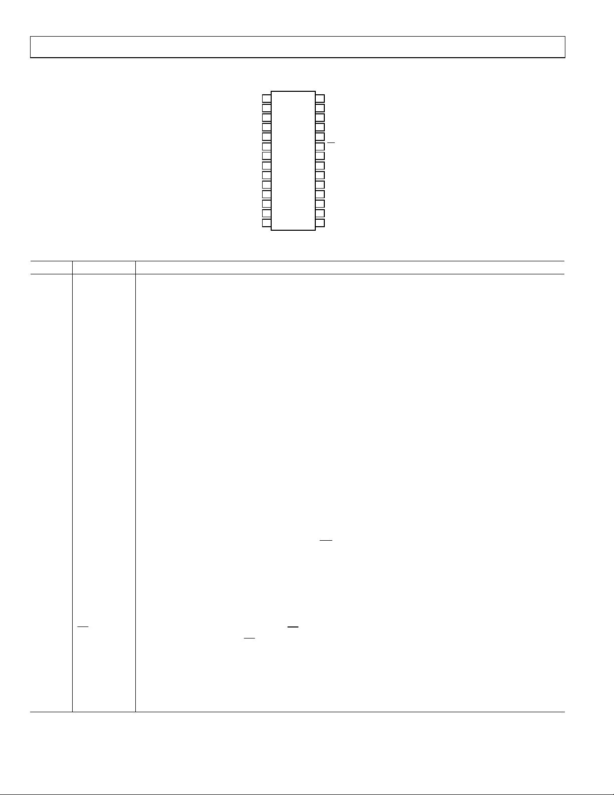
PIN CONFIGURATION AND FUNCTION DESCRIPTIONS
1
CS5
FB5
2
EAN5
3
EAO5
4
ADP3026
5
SS5
CLSET5
REF
AGND
CLSET3
SS3
EAO3
EAN3
FB3
CS3
TOP VIEW
6
(Not to Scale)
7
8
9
10
11
12
13
14
Figure 2. 28-Lead TSSOP Pin Configuration
Table 3. Pin Function Descriptions
Pin No. Mnemonic Function
1 CS5
Current Sense Input for the Top N-Channel MOSFET of the 5 V Buck Converter. Connect to the drain of the top
N-channel MOSFET.
2 FB5 Feedback Input for the 5 V Buck Converter. Connect to the output sense point in fixed output mode.
3 EAN5 Inverting Input of the Error Amplifier of the 5 V Buck Converter. Use for external loop compensation.
4 EAO5 Error Amplifier Output for the 5 V Buck Converter.
5 SS5 Soft Start for the 5 V Buck Converter. Also used as an on/off pin.
6 CLSET5
Current Limit Setting. A resistor can be connected from AGND to CLSET5. A minimum current limit is obtained
by leaving it unconnected. A maximum current limit is obtained by connecting it to AGND.
7 REF
800 mV Band Gap Reference. Bypass it with a capacitor (22 nF typical) to AGND. REF cannot be used directly
with an external load.
8 AGND Analog Signal Ground.
9 CLSET3
Current Limit Setting. A resistor can be connected from AGND to CLSET3. A minimum current limit is obtained
by leaving it unconnected. A max current limit is obtained by connecting it to AGND.
10 SS3 Soft Start for the 3.3 V Buck Converter. Also used as an on/off pin.
11 EAO3 Error Amplifier Output for the 3.3 V Buck Converter.
12 EAN3 Error Amplifier Inverting Input of the 3.3 V Buck Converter. Use for external loop compensation.
13 FB3 Feedback Input for the 3.3 V Buck Converter. Connect to output sense point.
14 CS3
Current Sense Input for the Top N-Channel MOSFET of the 3.3 V Buck Converter. It should be connected to the
drain of the N-channel MOSFET.
15 PWRGD
Power Good Output. PWRGD goes low with no delay whenever the 5 V output drops 7% below its nominal
value. When the 5 V output is within −3% of its nominal value, PWRGD will be released after a time delay
determined by the timing capacitor on the CPOR pin.
16 CPOR
Connect a capacitor between CPOR and AGND to set the delay time for the PWRGD pin. A 1 µA pull-up current
is used to charge the capacitor. A manual reset (
17 BST3 Boost Capacitor Connection for High-Side Gate Driver of the 3.3 V Buck Converter.
18 DRVH3 High-Side Gate Driver for the 3.3 V Buck Converter.
19 SW3 Switching Node (Inductor) Connection of the 3.3 V Buck Converter.
20 DRVL3 Low-Side Gate Driver of the 3.3 V Buck Converter.
21 VIN Main Supply Input (5.5 V to 25 V).
22 INTVCC Linear Regulator Bypass for the internal 5 V LDO. Bypass this pin with a 4.7 µF capacitor to AGND.
23
SD
Shutdown Control Input, Active Low. If
SD
automatic startup, connect
to VIN directly.
24 PGND Power Ground.
25 DRVL5 Low-Side Driver for the 5 V Buck Converter.
26 SW5 Switching Node (Inductor) Connection for the 5 V Buck Converter.
27 DRVH5 High-Side Gate Driver for the 5 V Buck Converter.
28 BST5 Boost Capacitor Connection for the High-Side Gate Driver of the 5 V Buck Converter.
28
BST5
DRVH5
27
SW5
26
DRVL5
25
24
PGND
23
SD
INTVCC
22
VIN
21
DRVL3
20
19
SW3
18
DRVH3
BST3
17
CPOR
16
PWRGD
15
MR
SD
= 0 V, the chip is in shutdown with very low quiescent current. For
02950-002
) function can also be implemented by grounding this pin.
Rev. 0 | Page 6 of 20
 Loading...