Analog Devices ADP3025 a Datasheet
High Efficiency Dual Output
FEATURES
Wide input voltage range: 5.5 V to 25 V
High conversion efficiency > 96%
Integrated current sense—no external resistor required
Low shutdown current: 19 µA (typical)
Voltage mode PWM with input feed-forward for fast line
transient response
Dual synchronous buck controllers
Built-in gate drive boost circuit for driving external high-side
N-channel MOSFET
2 independently programmable output voltages:
Fixed 3.3 V or adjustable (800 mV to 6.0 V)
Fixed 5 V or adjustable (800 mV to 6.0 V)
Programmable PWM frequency
Integrated linear regulator controller
Extensive circuit protection functions
APPLICATIONS
Portable instruments
General-purpose dc-to-dc converters
Power Supply Controller
ADP3025
GENERAL DESCRIPTION
The ADP3025 is a highly efficient, dual synchronous buck
switching regulator controller optimized for converting a
battery or adapter input into the supply voltage required in
portable products and industrial systems. The oscillator
frequency can be programmed for 200 kHz or 300 kHz
operation, or can be synchronized to an external clock signal of
up to 350 kHz.
The ADP3025 provides accurate and reliable short-circuit
protection by using an internal current sense circuit that
reduces cost and increases overall efficiency. Other protection
features include programmable soft start, UVLO, and integrated
output undervoltage/overvoltage protection. The ADP3025
contains a linear regulator controller designed to drive an
external N-channel MOSFET. The linear regulator output is
adjustable and can be used to generate auxiliary supply voltages.
The ADP3025 is specified over the 0°C to 70°C commercial
temperature range and is available in a 38-lead TSSOP package.
V
5.5V TO 25V
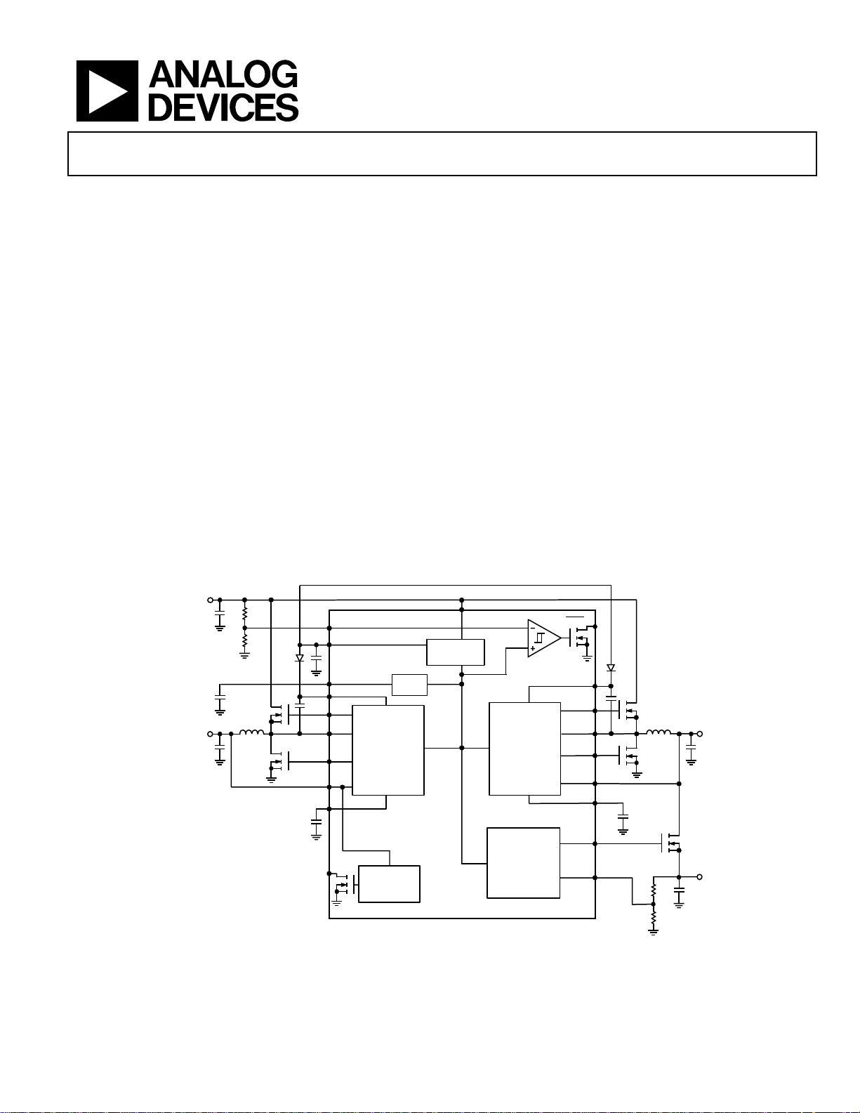
SIMPLIFIED FUNCTIONAL BLOCK DIAGRAM
IN
PFO
5V LINEAR
REGULATOR
REF
Q3
5V
L2
Q4
SS5
PWRGD
5V
SWITCHING
CONTROLLER
POWER-ON
RESET
ADP3025
Figure 1.
800mV
3.3V
3.3V
SWITCHING
SWITCHING
CONTROLLER
CONTROLLER
LINEAR
CONTROLLER
SS3
Q1
L1
Q2
3.3V
Q5
2.5V
02699-0-001
Rev. A
Information furnished by Analog Devices is believed to be accurate and reliable.
However, no responsibility is assumed by Analog Devices for its use, nor for any
infringements of patents or other rights of third parties that may result from its use.
Specifications subject to change without notice. No license is granted by implication
or otherwise under any patent or patent rights of Analog Devices. Trademarks and
registered trademarks are the property of their respective owners.
One Technology Way, P.O. Box 9106, Norwood, MA 02062-9106, U.S.A.
Tel: 781.329.4700
Fax: 781.326.8703 © 2004 Analog Devices, Inc. All rights reserved.
www.analog.com

ADP3025
TABLE OF CONTENTS
Specifications..................................................................................... 3
Output Voltage Adjustment ...................................................... 13
Absolute Maximum Ratings............................................................ 5
ESD Caution.................................................................................. 5
Pin Configuration and Function Descriptions............................. 6
Typical Performance Characteristics ............................................. 9
Theory of Operation ...................................................................... 11
Internal 5 V Supply (INTVCC) ................................................ 11
Reference (REF).......................................................................... 11
Boosted High-Side Gate Drive Supply (BST)......................... 11
Synchronous Rectifier (DRVL) ................................................11
Oscillator Frequency and Synchronization (SYNC).............. 11
Shutdown SD............................................................................... 11
Soft Start and Power-Up Sequencing (SS) .............................. 11
Current Limiting (CLSET)........................................................ 12
Output Undervoltage Protection.............................................. 12
Output Overvoltage and Reverse Voltage Protection............ 12
Application Information ........................................................... 13
Input Voltage Range ................................................................... 13
Maximum Output Current and MOSFET Selection............. 14
Nominal Inductor Value............................................................ 15
Inductor Selection...................................................................... 15
CIN and C
Power MOSFET Selection......................................................... 16
Soft Start ...................................................................................... 17
Fixed or Adjustable Output Voltage......................................... 17
Efficiency Enhancement............................................................ 17
Transient Response Considerations......................................... 18
Feedback Loop Compensation................................................. 18
Compensation Loop Design and Test Method ...................... 19
Recommended Applications..................................................... 19
Layout Considerations............................................................... 19
Selection............................................................... 16
OUT
Power Good Output (PWRGD)............................................... 12
Linear Regulator Controller...................................................... 12
Outline Dimensions....................................................................... 21
Ordering Guide .......................................................................... 21
REVISION HISTORY
Revision A
4/04—Data Sheet changed from Rev. 0 to Rev. A
Change Page
Changes to Features...................................................................... 1
Changes to Specifications............................................................ 3
Changes to Figures 4 and 5.......................................................... 9
Changes to Theory of Operation section ................................11
Changes to Output Voltage Adjustment section .................... 13
Changes to Table 5...................................................................... 13
Changes to Table 6...................................................................... 15
Changes to Table 8...................................................................... 16
Changes to Table 9...................................................................... 17
1/04—Revision 0: Initial Version
Rev. A | Page 2 of 24
ADP3025
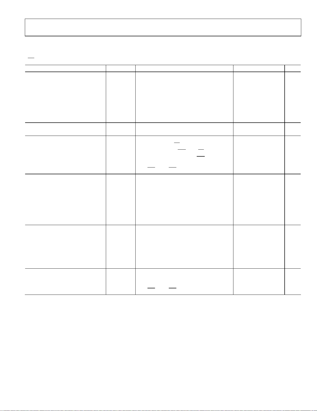
SPECIFICATIONS1
Table 1. TA = 0°C to 70°C, V
= 5 V, unless otherwise noted
SD
Parameter Symbol Conditions Min Typ Max Unit
INTERNAL 5 V REGULATOR INTVCC
Input Voltage Range 5.5 25 V
Output Voltage TA = 25°C 4.95 5.02 5.15 V
Line Regulation 5.5 V ≤ VIN ≤ 25 V 1.0 mV/V
Total Variation Full VIN and temperature range 4.8 5.2 V
VIN Undervoltage Lockout V
Threshold Voltage 4.05 4.25 4.5 V
Hysteresis 270 mV
REFERENCE
Output Voltage2 REF 5.5 V ≤ VIN ≤ 25 V 784 800 816 mV
SUPPLY IQ
Shutdown Current
Standby Current
Quiescent Current
OSCILLATOR
Frequency f
SYNC = INTVCC, 5.5 V ≤ VIN ≤ 25 V 250 300 350 kHz
SYNC Input
Frequency Range 230 350 kHz
Input Low Voltage3 t
Input High Voltage3 t
Input Current SYNC = 5 V 0.5 µA
POWER GOOD PWRGD
Output Voltage in Regulation 10 kΩ pull-up to 5 V 4.8 V
Output Voltage out of Regulation
PWRGD Trip Threshold FB5 rising; with respect to nominal output –6.0 –3.7 –1.5 %
PWRGD Hysteresis FB5 falling; with respect to nominal output 4 %
CPOR Pull-Up Current CPOR = 1.2 V –3.0 –1 –0.3 µA
ERROR AMPLIFIER
DC Gain3 47 dB
Gain-Bandwidth Product3 GBW 10 MHz
Input Leakage Current I
= 12 V, SS5 = SS3 = INTVCC, INTVCC Load = 0 mA, REF Load = 0 mA, SYNC = 0 V,
IN
INTVCC falling
UVLO
5.5 V ≤ VIN ≤ 25 V, SD
SS3 = SS5 = COMP2/SD2
= 0 V
= 0 V, SD = 5 V
No loads, SS3 = SS5 = COMP2/SD2
= 4 V,
19 70 µA
120 200 µA
1.3 1.9 mA
FB5 = 810 mV, FB3 = 810 mV, FB2 = 810 mV,
ADJ/FX5
SYNC = AGND, 5.5 V ≤ VIN ≤ 25 V 175 210 245 kHz
OSC
10 kΩ pull-up to 5 V, FB5 < 90% of nominal
= ADJ/FX3 = 5 V
≤ 200 ns 0.4 V
F
≤ 200 ns 2.8 V
R
0.4 V
output value
EAN
ADJ/FX5
= ADJ/FX3 = 5 V
200 nA
Rev. A | Page 3 of 24
ADP3025
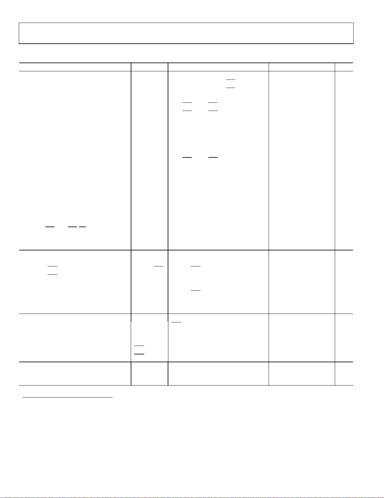
SPECIFICATIONS (continued)
Parameter Symbol Conditions Min Typ Max Unit
MAIN SMPS CONTROLLERS
Fixed 5 V Output Voltage FB5
Fixed 3.3 V Output Voltage FB3
Adjustable Output Voltage FB5, FB3
Output Voltage Adjustment Range3
5.5 V ≤ VIN ≤ 25 V, ADJ/FX5
5.5 V ≤ VIN ≤ 25 V, ADJ/FX3
5.5 V ≤ VIN ≤ 25 V,
ADJ/FX5
ADJ/FX5
= ADJ/FX3 = 5 V
= ADJ/FX3 = 5 V
= 0 V
= 0 V
Current Limit Threshold
CLSET5 = CLSET3 = Floating 5.5 V = VIN = 25 V, TA = 25°C 54 72 90 mV
CLSET5 = CLSET3 = 0 V 5.5 V ≤ VIN ≤ 25 V, TA = 25°C 240 300 360 mV
Soft Start Current SS3 = SS5 = 3 V 0.7 2.1 3.8 µA
Soft Start Turn-On Threshold SS5, SS3 0.4 0.6 0.8 V
Feedback Input Leakage Current IFB
Maximum Duty Cycle3 D
VIN = 5.5 V, SYNC = AGND 94 99 %
MAX
ADJ/FX5
= ADJ/FX3 = 5 V, FB = 800 mV
Transition Time (DRVL)
Rise tR(DRVL) C
Fall tF(DRVL) C
= 3000 pF, 10% to 90% 40 70 ns
LOAD
= 3000 pF, 90% to 10% 45 70 ns
LOAD
Transition Time (DRVH)
Rise tR(DRVH) C
Fall tF(DRVH) C
= 3000 pF, 10% to 90% 50 100 ns
LOAD
= 3000 pF, 90% to 10% 50 100 ns
LOAD
Logic Input Voltage
ADJ/FX3, ADJ/FX5, SD
Logic Low VIL 0.6 V
Logic High VIH 2.9 V
LINEAR REGULATOR CONTROLLER
Feedback Threshold FB2 776 800 824 mV
COMP2/SD2 Pull-Up Current COMP2/SD2 COMP2/SD2 = 0 V
COMP2/SD2 Threshold
0.5 0.85 1.1 V
DC Gain3 62 dB
Transconductance g
3
m
COMP2/SD2
= 3 V
Gain-Bandwidth Product3 GBW 20 MHz
FB2 Input Leakage Current I
FB2 = 800 mV 20 nA
FB2
POWER-FAIL COMPARATOR
PFI Input Threshold PFI
from high to low
PFO
PFI Input Hysteresis 14 mV
PFI Input Current I
PFO High Voltage
PFO Low Voltage
500 nA
PFI
PFO
PFO
H
L
10 kΩ pull-up to 5 V 4.8 V
10 kΩ pull-up to 5 V 0.4 V
FAULT PROTECTION
Output Overvoltage Trip Threshold With respect to nominal output 115 120 125 %
Output Undervoltage Lockout Threshold With respect to nominal output 70 80 90 %
1
All limits at temperature extremes are guaranteed via correlation using standard statistical quality control (SQC) methods.
2
The reference’s line regulation error is insignificant. The reference is not supposed to be loaded externally.
3
Guaranteed by design, not tested in production.
4.90 5.0 5.10 V
3.234 3.3 3.366 V
776 800 824 mV
0.800 6.0 V
600 nA
2.8 µA
0.3 ms
776 800 824 mV
Rev. A | Page 4 of 24
ADP3025
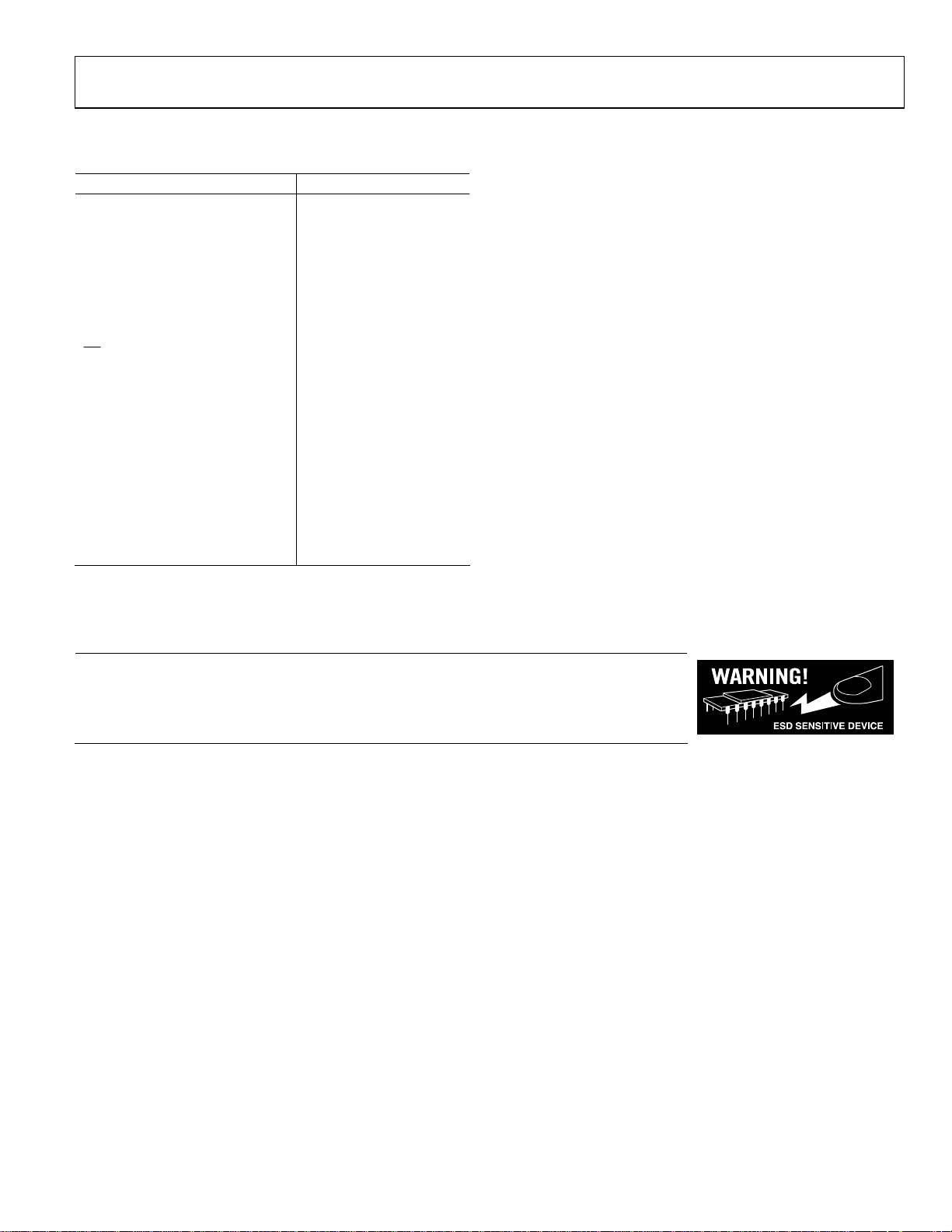
ABSOLUTE MAXIMUM RATINGS
Table 2. ADP3025 Stress Ratings
Parameter Rating
VIN to AGND –0.3 V to +27 V
AGND to PGND ±0.3 V
INTVCC AGND – 0.3 V to +6 V
BST5, BST3 to PGND –0.3 V to +32 V
BST5 to SW5 –0.3 V to +6 V
BST3 to SW3 –0.3 V to +6 V
CS5, CS3 AGND – 0.3 V to VIN
SW3, SW5 to PGND –2 V to VIN + 0.3 V
SD
DRVL5/3 to PGND –0.3 V to INTVCC + 0.3 V
DRVH5/3 to SW5/3 –0.3 V to INTVCC + 0.3 V
All Other Inputs and Outputs
θ
JA
Operating Ambient Temperature
Range 0°C to 70°C
Junction Temperature Range 0°C to 150°C
Storage Temperature Range –65°C to +150°C
Lead Temperature Range
(Soldering 10 sec) 300°C
AGND – 0.3 V to +27 V
AGND – 0.3 V to
INTVCC + 0.3 V
98°C/W
Stresses above those listed under Absolute Maximum Ratings
may cause permanent damage to the device. This is a stress
rating only; functional operation of the device at these or any
other conditions above those listed in the operational sections
of this specification is not implied. Exposure to absolute
maximum rating conditions for extended periods may affect
device reliability.
ESD CAUTION
ESD (electrostatic discharge) sensitive device. Electrostatic charges as high as 4000 V readily
accumulate on the human body and test equipment and can discharge without detection. Although
this product features proprietary ESD protection circuitry, permanent damage may occur on devices
subjected to high energy electrostatic discharges. Therefore, proper ESD precautions are
recommended to avoid performance degradation or loss of functionality.
Rev. A | Page 5 of 24
ADP3025
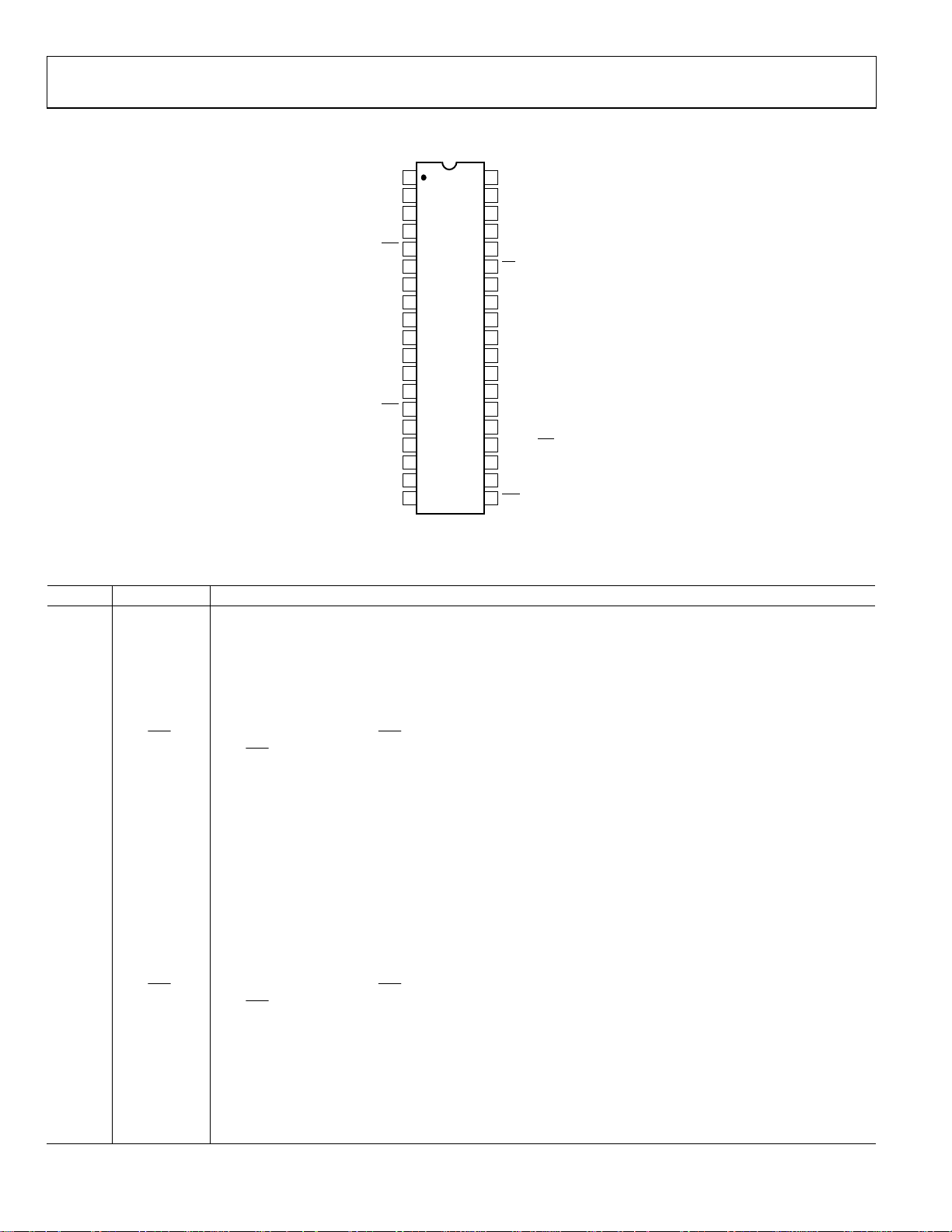
PIN CONFIGURATION AND FUNCTION DESCRIPTIONS
CS5
FB5
EAN5
EAO5
ADJ/FX5
SS5
CLSET5
REF
AGND
CLSET3
INTVCC2
SYNC
SS3
ADJ/FX3
EAO3
EAN3
FB3
CS3
PFI
1
2
3
4
5
6
ADP3025
7
TOP VIEW
8
(Not to Scale)
9
10
11
12
13
14
15
16
17
18
19
BST5
38
DRVH5
37
36
SW5
35
DRVL5
34
PGND1
33
SD
32
PGND2
31
INTVCC1
30
VIN
29
DRVL3
28
SW3
27
DRVH3
26
BST3
25
DRV2
24
FB2
COMP2/SD2
23
22
CPOR
21
PWRGD
20
PFO
02699-0-002
Figure 2. 38-Lead TSSOP Pin Configuration
Table 3. Pin Function Descriptions
Pin No. Mnemonic Function
1 CS5
Current Sense Input for the Top N-Channel MOSFET of the 5 V Buck Converter. Connect to the drain of the top
N-channel MOSFET.
2 FB5
Feedback Input for the 5 V Buck Converter. Connect to the output sense point in fixed output mode. Connect to
an external resistor divider in adjustable output mode.
3 EAN5
Inverting Input of the Error Amplifier of the 5 V Buck Converter. Use for external loop compensation only in
fixed output mode. In adjustable output mode, connect to the external resistor divider.
4 EAO5 Error Amplifier Output for the 5 V Buck Converter.
5
FX5 TTL Logic Input. When ADJ/FX5 = 0 V, fixed output mode, connect FB5 to the output sense point. When
ADJ/
FX5 = 5 V, adjustable output mode, connect FB5 to the external resistor divider.
ADJ/
6 SS5 Soft Start for the 5 V Buck Converter. Also used as an ON/OFF pin.
7 CLSET5
Current Limit Setting. A resistor can be connected from AGND to CLSET5. A minimum current limit is obtained
by leaving it open. A maximum current limit is obtained by connecting it to AGND.
8 REF 800 mV Reference. Bypass it with a capacitor (22 nF typical) to AGND. REF cannot be loaded externally.
9 AGND Analog Signal Ground.
10 CLSET3
Current Limit Setting. A resistor can be connected from AGND to CLSET3. A minimum current limit is obtained
by leaving it open. A maximum current limit is obtained by connecting it to AGND.
11, 31 INTVCC2, 1
Linear Regulator Bypass for the Internal 5 V LDO. Bypass this pin with a 4.7 µF capacitor to AGND. Pins 11 and 31
must be connected for proper operation.
12 SYNC
Oscillator Synchronization and Frequency Select. f
= 200 kHz when SYNC = 0 V; select f
OSC
= 300 kHz, when
OSC
SYNC = 5 V. The oscillator can be synchronized with an external source through the SYNC pin.
13 SS3 Soft Start for the 3.3 V Buck Converter. Also used as an ON/OFF pin.
14
FX3 TTL Logic Input. When ADJ/FX3 = 0 V, fixed output mode, connect FB3 to the output sense point. When
ADJ/
ADJ/
FX3 = 5 V, adjustable output mode, connect FB3 to the external resistor divider.
15 EAO3 Error Amplifier Output for the 3.3 V Buck Converter.
16 EAN3
Error Amplifier Inverting Input of the 3.3 V Buck Converter. Use for external loop compensation only in fixed
output mode. In adjustable output mode, connect to an external resistor divider.
17 FB3
Feedback Input for the 3.3 V Buck Converter. Connect to output sense point in fixed output mode. Connect to
an external resistor divider in adjustable output mode.
18 CS3
Current Sense Input for the Top N-Channel MOSFET of the 3.3 V Buck Converter. CS3 should be connected to
the drain of the N-channel MOSFET.
Rev. A | Page 6 of 24

ADP3025
Pin No. Mnemonic Function
19 PFI
20
21 PWRGD
22 CPOR
23
24 FB2 Feedback for the Linear Regulator Controller.
25 DRV2 NMOS Gate Drive Output for the Linear Regulator Controller.
26 BST3 Boost Capacitor Connection for High-Side Driver of the 3.3 V Buck Converter.
27 DRVH3 High-Side Gate Drive for the 3.3 V Buck Converter.
28 SW3 Switching Node (Inductor) Connection of the 3.3 V Buck Converter.
29 DRVL3 Low-Side Gate Drive of the 3.3 V Buck Converter.
30 VIN Main Supply Input (5.5 V to 25 V).
32, 34 PGND2, 1 Power Ground. Pins 32 and 34 must be connected together for proper operation.
33
35 DRVL5 Low-Side Gate Drive for the 5 V Buck Converter.
36 SW5 Switching Node (Inductor) Connection for the 5 V Buck Converter.
37 DRVH5 High-Side Gate Drive for the 5 V Buck Converter.
38 BST5 Boost Capacitor Connection for the High-Side Driver of the 5 V Buck Converter.
PFO Power Failure Output, Open Drain Output. This pin sinks current when the PFI pin is lower than 800 mV.
COMP2/
SD Shutdown Control Input, Active Low. If SD = 0 V, the chip is in shutdown mode with very low quiescent current.
SD2 Compensation Input for the Linear Regulator Controller. Connect an RC network to GND for stable operation.
Negative Input of a Comparator that can be Used as a Power-Fail Detector. The positive input is connected to
the 800 mV reference. There is a 14 mV hysteresis for this comparator.
Otherwise,
Power Good Output. PWRGD goes low with no delay whenever the 5 V output drops 7% below its nominal
value. When the 5 V output is within –3% of its nominal value, PWRGD is released after a time delay determined
by the timing capacitor on the CPOR pin.
Power-On Reset Capacitor. Connect a capacitor between CPOR and AGND to set the delay time for the PWRGD
pin. A 1 µA pull-up current is used to charge the capacitor. A manual reset (
by pulling this pin low.
This pin is also used as an ON/OFF pin of the linear regulator controller.
For automatic startup, connect
PFO is floating.
MR) function can also be achieved
SD to VIN via a resistor.
Rev. A | Page 7 of 24
ADP3025
2
INPUT
5V
.5V
3.3V
COMP2/SD2
SD
INTVCC1
INTVCC2
REF
AGND
PFO
PFI
SYNC
PWRGD
CPOR
DRV2
FB2
PGND
33
31
11
8
9
20
19
12
21
22
25
24
23
0.8V
0.8V
LINEAR REG
800mV
REF
–
+
200kHz/
300kHz/
OSC
POWER-
ON
RESET
1µA
–
g
m
+
+5V
UVLO
FB5
×1
SHUTDOWN
S
Q
R
VIN
30
ADP3025
CONTROL
LOGIC
OC
OC
EA
816mV
+
–
800mV
+
–
+
792mV
–
–
800mV
+
960mV
+
–
640mV
+
–
1.8V
–
+
+
–
INTVCC
0.6V
72mV
–
+
+
–
14mV
–
+
+
–
+
–
–3mV
0.7µA
2.1µA
1
CLSET5
7
38
37
36
35
34
32
2
3
4
5
6
CS5
BST5
DRVH5
SW5
DRVL5
PGND1
PGND2
FB5
EAN5
EAO5
ADJ/FX5
SS5
V
5V
OUT5
DUPLICATE FOR SECOND CONTROLLER
02699-0-003
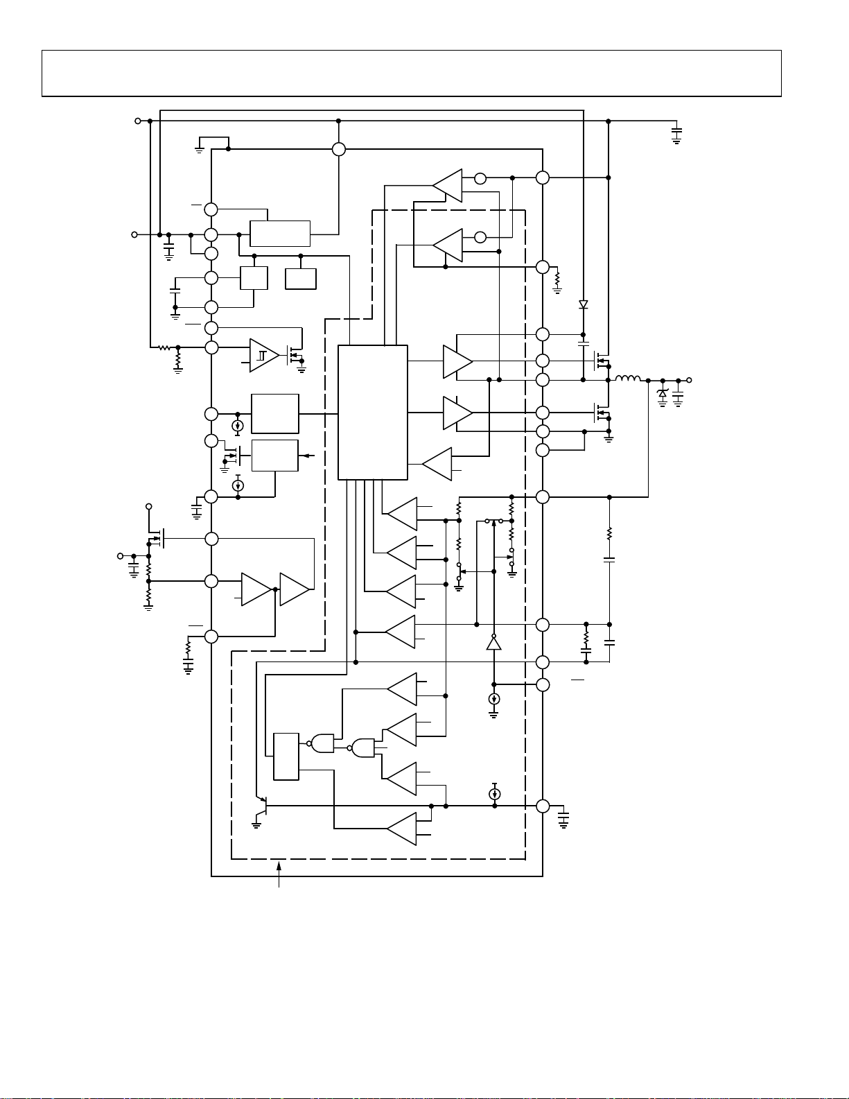
Figure 3. Block Diagram (All Switches and Components Shown for Fixed Output Operation)
Rev. A | Page 8 of 24
 Loading...