

High Efficiency Dual Output
FEATURES
Wide input voltage range: 5.5 V to 25 V
High conversion efficiency > 96%
Integrated current sense—no external resistor required
Low shutdown current: 19 µA (typical)
Voltage mode PWM with input feed-forward for fast line
transient response
Dual synchronous buck controllers
Built-in gate drive boost circuit for driving external high-side
N-channel MOSFET
2 independently programmable output voltages:
Fixed 3.3 V or adjustable (800 mV to 6.0 V)
Fixed 5 V or adjustable (800 mV to 6.0 V)
Programmable PWM frequency
Integrated linear regulator controller
Extensive circuit protection functions
APPLICATIONS
Portable instruments
General-purpose dc-to-dc converters
Power Supply Controller
ADP3025
GENERAL DESCRIPTION
The ADP3025 is a highly efficient, dual synchronous buck
switching regulator controller optimized for converting a
battery or adapter input into the supply voltage required in
portable products and industrial systems. The oscillator
frequency can be programmed for 200 kHz or 300 kHz
operation, or can be synchronized to an external clock signal of
up to 350 kHz.
The ADP3025 provides accurate and reliable short-circuit
protection by using an internal current sense circuit that
reduces cost and increases overall efficiency. Other protection
features include programmable soft start, UVLO, and integrated
output undervoltage/overvoltage protection. The ADP3025
contains a linear regulator controller designed to drive an
external N-channel MOSFET. The linear regulator output is
adjustable and can be used to generate auxiliary supply voltages.
The ADP3025 is specified over the 0°C to 70°C commercial
temperature range and is available in a 38-lead TSSOP package.
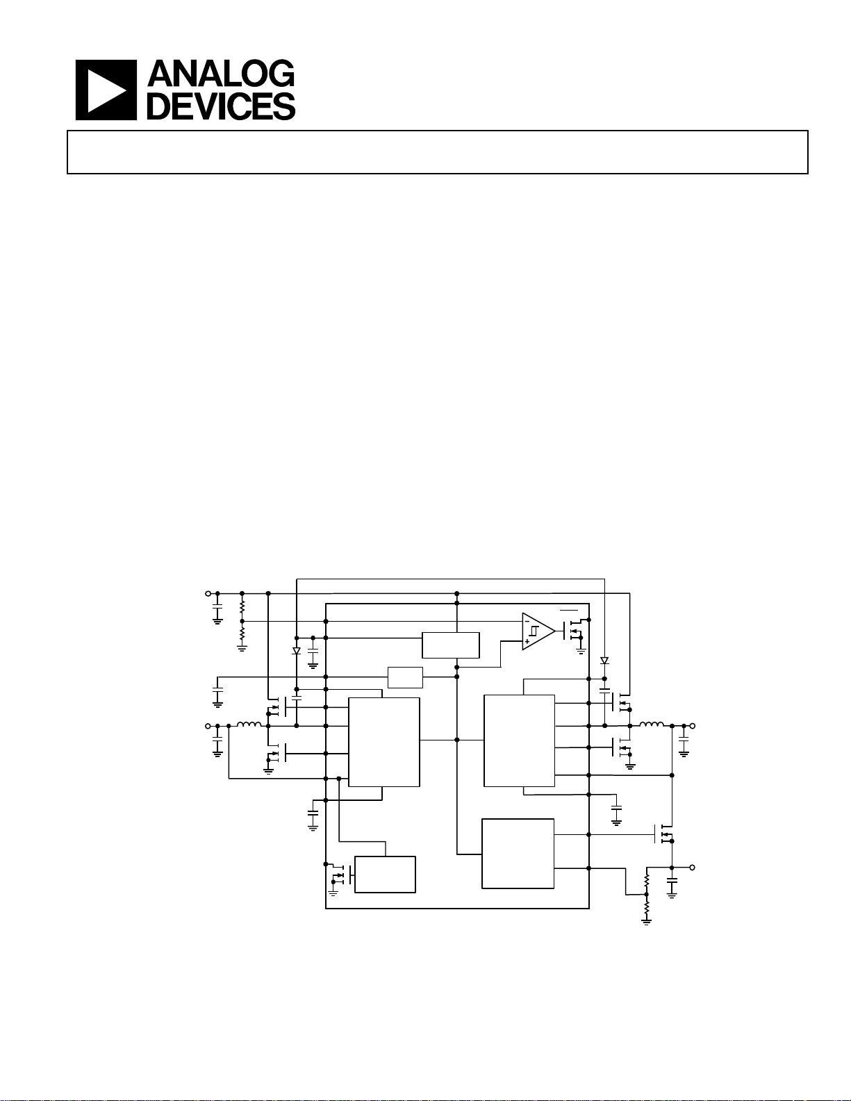
V
5.5V TO 25V
SIMPLIFIED FUNCTIONAL BLOCK DIAGRAM
IN
PFO
5V LINEAR
REGULATOR
REF
Q3
5V
L2
Q4
SS5
PWRGD
5V
SWITCHING
CONTROLLER
POWER-ON
RESET
ADP3025
Figure 1.
800mV
3.3V
3.3V
SWITCHING
SWITCHING
CONTROLLER
CONTROLLER
LINEAR
CONTROLLER
SS3
Q1
L1
Q2
3.3V
Q5
2.5V
02699-0-001
Rev. A
Information furnished by Analog Devices is believed to be accurate and reliable.
However, no responsibility is assumed by Analog Devices for its use, nor for any
infringements of patents or other rights of third parties that may result from its use.
Specifications subject to change without notice. No license is granted by implication
or otherwise under any patent or patent rights of Analog Devices. Trademarks and
registered trademarks are the property of their respective owners.
One Technology Way, P.O. Box 9106, Norwood, MA 02062-9106, U.S.A.
Tel: 781.329.4700
Fax: 781.326.8703 © 2004 Analog Devices, Inc. All rights reserved.
www.analog.com

ADP3025
TABLE OF CONTENTS
Specifications..................................................................................... 3
Output Voltage Adjustment ...................................................... 13
Absolute Maximum Ratings............................................................ 5
ESD Caution.................................................................................. 5
Pin Configuration and Function Descriptions............................. 6
Typical Performance Characteristics ............................................. 9
Theory of Operation ...................................................................... 11
Internal 5 V Supply (INTVCC) ................................................ 11
Reference (REF).......................................................................... 11
Boosted High-Side Gate Drive Supply (BST)......................... 11
Synchronous Rectifier (DRVL) ................................................11
Oscillator Frequency and Synchronization (SYNC).............. 11
Shutdown SD............................................................................... 11
Soft Start and Power-Up Sequencing (SS) .............................. 11
Current Limiting (CLSET)........................................................ 12
Output Undervoltage Protection.............................................. 12
Output Overvoltage and Reverse Voltage Protection............ 12
Application Information ........................................................... 13
Input Voltage Range ................................................................... 13
Maximum Output Current and MOSFET Selection............. 14
Nominal Inductor Value............................................................ 15
Inductor Selection...................................................................... 15
CIN and C
Power MOSFET Selection......................................................... 16
Soft Start ...................................................................................... 17
Fixed or Adjustable Output Voltage......................................... 17
Efficiency Enhancement............................................................ 17
Transient Response Considerations......................................... 18
Feedback Loop Compensation................................................. 18
Compensation Loop Design and Test Method ...................... 19
Recommended Applications..................................................... 19
Layout Considerations............................................................... 19
Selection............................................................... 16
OUT
Power Good Output (PWRGD)............................................... 12
Linear Regulator Controller...................................................... 12
Outline Dimensions....................................................................... 21
Ordering Guide .......................................................................... 21
REVISION HISTORY
Revision A
4/04—Data Sheet changed from Rev. 0 to Rev. A
Change Page
Changes to Features...................................................................... 1
Changes to Specifications............................................................ 3
Changes to Figures 4 and 5.......................................................... 9
Changes to Theory of Operation section ................................11
Changes to Output Voltage Adjustment section .................... 13
Changes to Table 5...................................................................... 13
Changes to Table 6...................................................................... 15
Changes to Table 8...................................................................... 16
Changes to Table 9...................................................................... 17
1/04—Revision 0: Initial Version
Rev. A | Page 2 of 24
ADP3025
SPECIFICATIONS1
Table 1. TA = 0°C to 70°C, V
= 5 V, unless otherwise noted
SD
Parameter Symbol Conditions Min Typ Max Unit
INTERNAL 5 V REGULATOR INTVCC
Input Voltage Range 5.5 25 V
Output Voltage TA = 25°C 4.95 5.02 5.15 V
Line Regulation 5.5 V ≤ VIN ≤ 25 V 1.0 mV/V
Total Variation Full VIN and temperature range 4.8 5.2 V
VIN Undervoltage Lockout V
Threshold Voltage 4.05 4.25 4.5 V
Hysteresis 270 mV
REFERENCE
Output Voltage2 REF 5.5 V ≤ VIN ≤ 25 V 784 800 816 mV
SUPPLY IQ
Shutdown Current
Standby Current
Quiescent Current
OSCILLATOR
Frequency f
SYNC = INTVCC, 5.5 V ≤ VIN ≤ 25 V 250 300 350 kHz
SYNC Input
Frequency Range 230 350 kHz
Input Low Voltage3 t
Input High Voltage3 t
Input Current SYNC = 5 V 0.5 µA
POWER GOOD PWRGD
Output Voltage in Regulation 10 kΩ pull-up to 5 V 4.8 V
Output Voltage out of Regulation
PWRGD Trip Threshold FB5 rising; with respect to nominal output –6.0 –3.7 –1.5 %
PWRGD Hysteresis FB5 falling; with respect to nominal output 4 %
CPOR Pull-Up Current CPOR = 1.2 V –3.0 –1 –0.3 µA
ERROR AMPLIFIER
DC Gain3 47 dB
Gain-Bandwidth Product3 GBW 10 MHz
Input Leakage Current I
= 12 V, SS5 = SS3 = INTVCC, INTVCC Load = 0 mA, REF Load = 0 mA, SYNC = 0 V,
IN
INTVCC falling
UVLO
5.5 V ≤ VIN ≤ 25 V, SD
SS3 = SS5 = COMP2/SD2
= 0 V
= 0 V, SD = 5 V
No loads, SS3 = SS5 = COMP2/SD2
= 4 V,
19 70 µA
120 200 µA
1.3 1.9 mA
FB5 = 810 mV, FB3 = 810 mV, FB2 = 810 mV,
ADJ/FX5
SYNC = AGND, 5.5 V ≤ VIN ≤ 25 V 175 210 245 kHz
OSC
10 kΩ pull-up to 5 V, FB5 < 90% of nominal
= ADJ/FX3 = 5 V
≤ 200 ns 0.4 V
F
≤ 200 ns 2.8 V
R
0.4 V
output value
EAN
ADJ/FX5
= ADJ/FX3 = 5 V
200 nA
Rev. A | Page 3 of 24
ADP3025
SPECIFICATIONS (continued)
Parameter Symbol Conditions Min Typ Max Unit
MAIN SMPS CONTROLLERS
Fixed 5 V Output Voltage FB5
Fixed 3.3 V Output Voltage FB3
Adjustable Output Voltage FB5, FB3
Output Voltage Adjustment Range3
5.5 V ≤ VIN ≤ 25 V, ADJ/FX5
5.5 V ≤ VIN ≤ 25 V, ADJ/FX3
5.5 V ≤ VIN ≤ 25 V,
ADJ/FX5
ADJ/FX5
= ADJ/FX3 = 5 V
= ADJ/FX3 = 5 V
= 0 V
= 0 V
Current Limit Threshold
CLSET5 = CLSET3 = Floating 5.5 V = VIN = 25 V, TA = 25°C 54 72 90 mV
CLSET5 = CLSET3 = 0 V 5.5 V ≤ VIN ≤ 25 V, TA = 25°C 240 300 360 mV
Soft Start Current SS3 = SS5 = 3 V 0.7 2.1 3.8 µA
Soft Start Turn-On Threshold SS5, SS3 0.4 0.6 0.8 V
Feedback Input Leakage Current IFB
Maximum Duty Cycle3 D
VIN = 5.5 V, SYNC = AGND 94 99 %
MAX
ADJ/FX5
= ADJ/FX3 = 5 V, FB = 800 mV
Transition Time (DRVL)
Rise tR(DRVL) C
Fall tF(DRVL) C
= 3000 pF, 10% to 90% 40 70 ns
LOAD
= 3000 pF, 90% to 10% 45 70 ns
LOAD
Transition Time (DRVH)
Rise tR(DRVH) C
Fall tF(DRVH) C
= 3000 pF, 10% to 90% 50 100 ns
LOAD
= 3000 pF, 90% to 10% 50 100 ns
LOAD
Logic Input Voltage
ADJ/FX3, ADJ/FX5, SD
Logic Low VIL 0.6 V
Logic High VIH 2.9 V
LINEAR REGULATOR CONTROLLER
Feedback Threshold FB2 776 800 824 mV
COMP2/SD2 Pull-Up Current COMP2/SD2 COMP2/SD2 = 0 V
COMP2/SD2 Threshold
0.5 0.85 1.1 V
DC Gain3 62 dB
Transconductance g
3
m
COMP2/SD2
= 3 V
Gain-Bandwidth Product3 GBW 20 MHz
FB2 Input Leakage Current I
FB2 = 800 mV 20 nA
FB2
POWER-FAIL COMPARATOR
PFI Input Threshold PFI
from high to low
PFO
PFI Input Hysteresis 14 mV
PFI Input Current I
PFO High Voltage
PFO Low Voltage
500 nA
PFI
PFO
PFO
H
L
10 kΩ pull-up to 5 V 4.8 V
10 kΩ pull-up to 5 V 0.4 V
FAULT PROTECTION
Output Overvoltage Trip Threshold With respect to nominal output 115 120 125 %
Output Undervoltage Lockout Threshold With respect to nominal output 70 80 90 %
1
All limits at temperature extremes are guaranteed via correlation using standard statistical quality control (SQC) methods.
2
The reference’s line regulation error is insignificant. The reference is not supposed to be loaded externally.
3
Guaranteed by design, not tested in production.
4.90 5.0 5.10 V
3.234 3.3 3.366 V
776 800 824 mV
0.800 6.0 V
600 nA
2.8 µA
0.3 ms
776 800 824 mV
Rev. A | Page 4 of 24
ADP3025
ABSOLUTE MAXIMUM RATINGS
Table 2. ADP3025 Stress Ratings
Parameter Rating
VIN to AGND –0.3 V to +27 V
AGND to PGND ±0.3 V
INTVCC AGND – 0.3 V to +6 V
BST5, BST3 to PGND –0.3 V to +32 V
BST5 to SW5 –0.3 V to +6 V
BST3 to SW3 –0.3 V to +6 V
CS5, CS3 AGND – 0.3 V to VIN
SW3, SW5 to PGND –2 V to VIN + 0.3 V
SD
DRVL5/3 to PGND –0.3 V to INTVCC + 0.3 V
DRVH5/3 to SW5/3 –0.3 V to INTVCC + 0.3 V
All Other Inputs and Outputs
θ
JA
Operating Ambient Temperature
Range 0°C to 70°C
Junction Temperature Range 0°C to 150°C
Storage Temperature Range –65°C to +150°C
Lead Temperature Range
(Soldering 10 sec) 300°C
AGND – 0.3 V to +27 V
AGND – 0.3 V to
INTVCC + 0.3 V
98°C/W
Stresses above those listed under Absolute Maximum Ratings
may cause permanent damage to the device. This is a stress
rating only; functional operation of the device at these or any
other conditions above those listed in the operational sections
of this specification is not implied. Exposure to absolute
maximum rating conditions for extended periods may affect
device reliability.
ESD CAUTION
ESD (electrostatic discharge) sensitive device. Electrostatic charges as high as 4000 V readily
accumulate on the human body and test equipment and can discharge without detection. Although
this product features proprietary ESD protection circuitry, permanent damage may occur on devices
subjected to high energy electrostatic discharges. Therefore, proper ESD precautions are
recommended to avoid performance degradation or loss of functionality.
Rev. A | Page 5 of 24
ADP3025
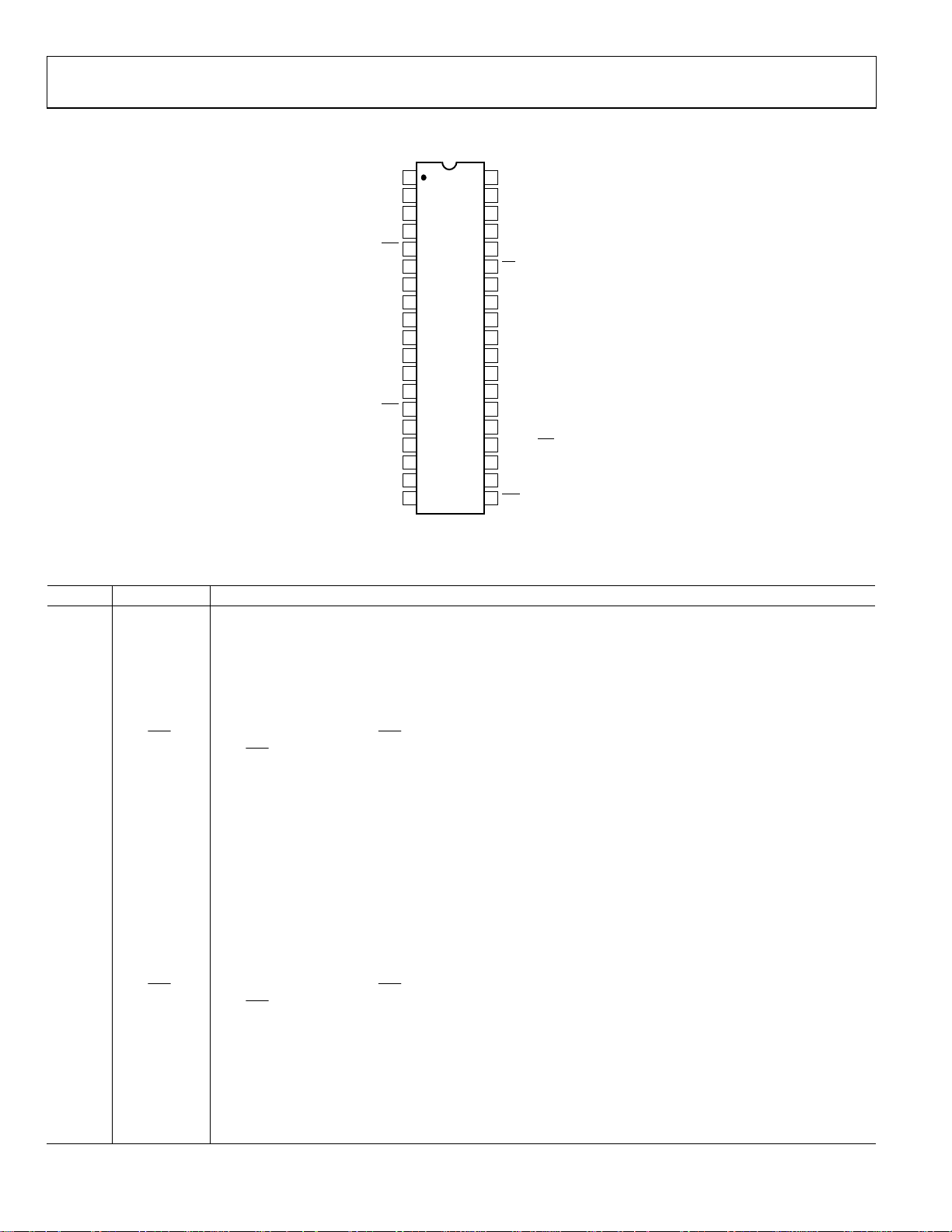
PIN CONFIGURATION AND FUNCTION DESCRIPTIONS
CS5
FB5
EAN5
EAO5
ADJ/FX5
SS5
CLSET5
REF
AGND
CLSET3
INTVCC2
SYNC
SS3
ADJ/FX3
EAO3
EAN3
FB3
CS3
PFI
1
2
3
4
5
6
ADP3025
7
TOP VIEW
8
(Not to Scale)
9
10
11
12
13
14
15
16
17
18
19
BST5
38
DRVH5
37
36
SW5
35
DRVL5
34
PGND1
33
SD
32
PGND2
31
INTVCC1
30
VIN
29
DRVL3
28
SW3
27
DRVH3
26
BST3
25
DRV2
24
FB2
COMP2/SD2
23
22
CPOR
21
PWRGD
20
PFO
02699-0-002
Figure 2. 38-Lead TSSOP Pin Configuration
Table 3. Pin Function Descriptions
Pin No. Mnemonic Function
1 CS5
Current Sense Input for the Top N-Channel MOSFET of the 5 V Buck Converter. Connect to the drain of the top
N-channel MOSFET.
2 FB5
Feedback Input for the 5 V Buck Converter. Connect to the output sense point in fixed output mode. Connect to
an external resistor divider in adjustable output mode.
3 EAN5
Inverting Input of the Error Amplifier of the 5 V Buck Converter. Use for external loop compensation only in
fixed output mode. In adjustable output mode, connect to the external resistor divider.
4 EAO5 Error Amplifier Output for the 5 V Buck Converter.
5
FX5 TTL Logic Input. When ADJ/FX5 = 0 V, fixed output mode, connect FB5 to the output sense point. When
ADJ/
FX5 = 5 V, adjustable output mode, connect FB5 to the external resistor divider.
ADJ/
6 SS5 Soft Start for the 5 V Buck Converter. Also used as an ON/OFF pin.
7 CLSET5
Current Limit Setting. A resistor can be connected from AGND to CLSET5. A minimum current limit is obtained
by leaving it open. A maximum current limit is obtained by connecting it to AGND.
8 REF 800 mV Reference. Bypass it with a capacitor (22 nF typical) to AGND. REF cannot be loaded externally.
9 AGND Analog Signal Ground.
10 CLSET3
Current Limit Setting. A resistor can be connected from AGND to CLSET3. A minimum current limit is obtained
by leaving it open. A maximum current limit is obtained by connecting it to AGND.
11, 31 INTVCC2, 1
Linear Regulator Bypass for the Internal 5 V LDO. Bypass this pin with a 4.7 µF capacitor to AGND. Pins 11 and 31
must be connected for proper operation.
12 SYNC
Oscillator Synchronization and Frequency Select. f
= 200 kHz when SYNC = 0 V; select f
OSC
= 300 kHz, when
OSC
SYNC = 5 V. The oscillator can be synchronized with an external source through the SYNC pin.
13 SS3 Soft Start for the 3.3 V Buck Converter. Also used as an ON/OFF pin.
14
FX3 TTL Logic Input. When ADJ/FX3 = 0 V, fixed output mode, connect FB3 to the output sense point. When
ADJ/
ADJ/
FX3 = 5 V, adjustable output mode, connect FB3 to the external resistor divider.
15 EAO3 Error Amplifier Output for the 3.3 V Buck Converter.
16 EAN3
Error Amplifier Inverting Input of the 3.3 V Buck Converter. Use for external loop compensation only in fixed
output mode. In adjustable output mode, connect to an external resistor divider.
17 FB3
Feedback Input for the 3.3 V Buck Converter. Connect to output sense point in fixed output mode. Connect to
an external resistor divider in adjustable output mode.
18 CS3
Current Sense Input for the Top N-Channel MOSFET of the 3.3 V Buck Converter. CS3 should be connected to
the drain of the N-channel MOSFET.
Rev. A | Page 6 of 24

ADP3025
Pin No. Mnemonic Function
19 PFI
20
21 PWRGD
22 CPOR
23
24 FB2 Feedback for the Linear Regulator Controller.
25 DRV2 NMOS Gate Drive Output for the Linear Regulator Controller.
26 BST3 Boost Capacitor Connection for High-Side Driver of the 3.3 V Buck Converter.
27 DRVH3 High-Side Gate Drive for the 3.3 V Buck Converter.
28 SW3 Switching Node (Inductor) Connection of the 3.3 V Buck Converter.
29 DRVL3 Low-Side Gate Drive of the 3.3 V Buck Converter.
30 VIN Main Supply Input (5.5 V to 25 V).
32, 34 PGND2, 1 Power Ground. Pins 32 and 34 must be connected together for proper operation.
33
35 DRVL5 Low-Side Gate Drive for the 5 V Buck Converter.
36 SW5 Switching Node (Inductor) Connection for the 5 V Buck Converter.
37 DRVH5 High-Side Gate Drive for the 5 V Buck Converter.
38 BST5 Boost Capacitor Connection for the High-Side Driver of the 5 V Buck Converter.
PFO Power Failure Output, Open Drain Output. This pin sinks current when the PFI pin is lower than 800 mV.
COMP2/
SD Shutdown Control Input, Active Low. If SD = 0 V, the chip is in shutdown mode with very low quiescent current.
SD2 Compensation Input for the Linear Regulator Controller. Connect an RC network to GND for stable operation.
Negative Input of a Comparator that can be Used as a Power-Fail Detector. The positive input is connected to
the 800 mV reference. There is a 14 mV hysteresis for this comparator.
Otherwise,
Power Good Output. PWRGD goes low with no delay whenever the 5 V output drops 7% below its nominal
value. When the 5 V output is within –3% of its nominal value, PWRGD is released after a time delay determined
by the timing capacitor on the CPOR pin.
Power-On Reset Capacitor. Connect a capacitor between CPOR and AGND to set the delay time for the PWRGD
pin. A 1 µA pull-up current is used to charge the capacitor. A manual reset (
by pulling this pin low.
This pin is also used as an ON/OFF pin of the linear regulator controller.
For automatic startup, connect
PFO is floating.
MR) function can also be achieved
SD to VIN via a resistor.
Rev. A | Page 7 of 24
ADP3025
2
INPUT
5V
.5V
3.3V
COMP2/SD2
SD
INTVCC1
INTVCC2
REF
AGND
PFO
PFI
SYNC
PWRGD
CPOR
DRV2
FB2
PGND
33
31
11
8
9
20
19
12
21
22
25
24
23
0.8V
0.8V
LINEAR REG
800mV
REF
–
+
200kHz/
300kHz/
OSC
POWER-
ON
RESET
1µA
–
g
m
+
+5V
UVLO
FB5
×1
SHUTDOWN
S
Q
R
VIN
30
ADP3025
CONTROL
LOGIC
OC
OC
EA
816mV
+
–
800mV
+
–
+
792mV
–
–
800mV
+
960mV
+
–
640mV
+
–
1.8V
–
+
+
–
INTVCC
0.6V
72mV
–
+
+
–
14mV
–
+
+
–
+
–
–3mV
0.7µA
2.1µA
1
CLSET5
7
38
37
36
35
34
32
2
3
4
5
6
CS5
BST5
DRVH5
SW5
DRVL5
PGND1
PGND2
FB5
EAN5
EAO5
ADJ/FX5
SS5
V
5V
OUT5
DUPLICATE FOR SECOND CONTROLLER
02699-0-003
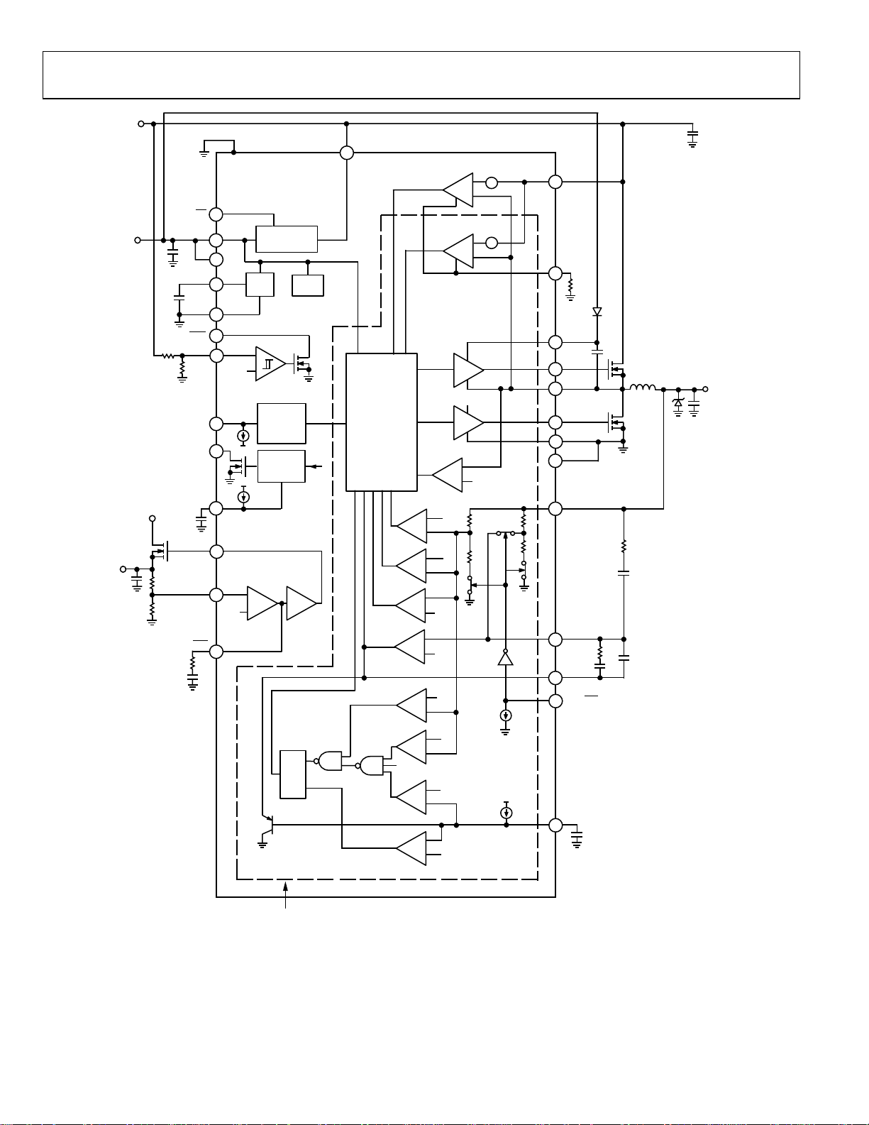
Figure 3. Block Diagram (All Switches and Components Shown for Fixed Output Operation)
Rev. A | Page 8 of 24

ADP3025
TYPICAL PERFORMANCE CHARACTERISTICS
100
190
EFFICIENCY (%)
EFFICIENCY (%)
100
A)
µ
CURRENT (
A)
µ
CURRENT (
170
150
130
110
90
70
50
0°C
+25°C
1051520
INPUT VOLTAGE (V)
Figure 7. Input Standby Current vs. Input Voltage
70
60
50
40
30
20
10
+70°C
25
02699-0-007
80
= 6.5V
V
IN
60
40
20
0
VIN = 15V
1023
OUTPUT CURRENT (A)
4
02699-0-004
Figure 4. Efficiency vs. 5 V Output Current
80
V
= 6.5V
IN
60
40
20
VIN = 15V
CURRENT (µA)
1800
1600
1400
1200
1000
0
1023
OUTPUT CURRENT (A)
4
02699-0-005
Figure 5. Efficiency vs. 3.3 V Output Current
+70°C
+25°C
0°C
1051520
INPUT VOLTAGE (V)
25
02699-0-006
Figure 6. Input Current vs. Input Voltage
0
1051520
INPUT VOLTAGE (V)
Figure 8. Input Shutdown Current vs. Input Voltage
310
=25V
V
305
300
FREQUENCY (kHz)
295
290
0 10203040506070
VIN=12V
AMBIENT TEMPERATURE (°C)
IN
V
=7.5V
V
=5.5V
IN
IN
Figure 9. Oscillator Frequency vs. Temperature
25
02699-0-008
02699-0-009
Rev. A | Page 9 of 24

ADP3025
400
CLSET = GND VIN= 5.5V TO 25V
350
300
250
CURRENT LIMIT THRESHOLD (mV)
200
010203040506070
AMBIENT TEMPERATURE (°C)
02699-0-010
Figure 10. Current Limit Threshold vs. Temperature
816
812
808
804
800
796
792
REFERENCE OUTPUT (mV)
788
784
0 10203040506070
AMBIENT TEMPERATURE (°C)
Figure 11. Reference Output vs. Temperature
02699-0-011
Figure 13. Load Transient Response—1 A to 3 A
Figure 14. Load Transient Response—3 A to 1 A
Figure 12. Soft Start Sequencing
Figure 15. V
= 7.5 V to 22 V Transient, 2.5 V Output, CH1—Input Voltage,
IN
CH2—Output Voltage
Rev. A | Page 10 of 24

ADP3025
THEORY OF OPERATION
The ADP3025 contains two synchronous step-down buck
controllers and a linear regulator controller. The buck controllers in the ADP3025 have the ability to provide either fixed
3.3 V and 5 V outputs or independently adjustable (800 mV to
6.0 V) outputs. Efficiency is improved by eliminating the
external current sense resistor, which is the main contributor to
loss during high current, low output voltage conditions.
INTERNAL 5 V SUPPLY (INTVCC)
An internal low dropout regulator (LDO) generates a 5 V
supply (INTVCC) that powers all the functional blocks within
the IC. The total current rating of this LDO is 50 mA. However,
this current is used for supplying gate drive power; current
should not be drawn from this pin for other purposes. Bypass
INTVCC to AGND with a 4.7 µF capacitor. A UVLO circuit is
also included in the regulator. When INTVCC < 4.05 V, the two
switching regulators and the linear regulator controller are shut
down. The UVLO hysteresis voltage is about 300 mV. The
internal LDO has a built-in foldback current limit so that it is
protected if a short circuit is applied to the 5 V output.
REFERENCE (REF)
The ADP3025 contains a precision 800 mV reference. Bypass
REF to AGND with a 22 nF ceramic capacitor. The reference is
intended for internal use only.
BOOSTED HIGH-SIDE GATE DRIVE SUPPLY (BST)
The gate drive voltage for the high-side N-channel MOSFET is
generated by a flying-capacitor boost circuit. The boost capacitor connected between BST and SW is charged from the
INTVCC supply. Use only small-signal diodes for the boost
circuit.
SYNCHRONOUS RECTIFIER (DRVL)
Synchronous rectification is used to reduce conduction losses
and ensure proper startup of the boost gate driver circuit.
Antishoot-through protection has been included to prevent
cross-conduction during switch transitions. The low-side driver
must be turned off before the high-side driver is turned on. For
typical N-channel MOSFETs, the dead time is approximately
50 ns. On the other edge, a dead time of approximately 50 ns is
achieved by an internal delay circuit. In discontinuous conduction mode (DCM), the synchronous rectifier is turned off when
the current flowing through the low-side MOSFET falls to zero.
In continuous conduction mode (CCM), the current flowing
through the low-side MOSFET never reaches zero, so the
synchronous rectifier is turned off by the next clock cycle.
OSCILLATOR FREQUENCY AND SYNCHRONIZATION (SYNC)
The SYNC pin controls the oscillator frequency. When SYNC =
0 V, f
= 200 kHz; when SYNC = 5 V, f
OSC
operation minimizes external component size and cost; 200 kHz
operation provides better efficiency and lower dropout. The
SYNC pin can also be used to synchronize the oscillator with an
external 5 V clock signal. A low-to-high transition on SYNC
initiates a new cycle. The synchronization range is 230 kHz to
350 kHz.
= 300 kHz. 300 kHz
OSC
SHUTDOWN SD
Holding SD low puts the ADP3025 into ultralow current shutdown mode. For automatic startup,
resistor.
can be tied to VIN via a
SD
SOFT START AND POWER-UP SEQUENCING (SS)
SS3 and SS5 are soft start pins for the two controllers. A 2 µA
pull-up current is used to charge an external soft start capacitor.
Power-up sequencing can easily be done by choosing different
capacitance. When SS3/SS5 < 0.6 V, the two switching regulators
are turned off. When 0.6 V < SS5/SS3 < 1.8 V, the regulators
start working in soft start mode. When SS3/SS5 > 1.8 V, the
regulators are in normal operating mode. The minimum soft
start time (~20 µs) is set by an internal capacitor. Table 4 shows
the ADP3025 operating modes.
Table 4. Operating Modes
SS5 SS3 Description
SD
Low All Circuits Turned Off
High SS5 < 0.6 V SS3 < 0.6 V 5 V and 3.3 V Off; INTVCC = 5 V, REF = 800 mV
High 0.6 V < SS5 < 1.8 V 5 V in Soft Start
High 1.8 V < SS5 5 V in Normal Operation
High 0.6 V < SS3 < 1.8 V 3.3 V in Soft Start
High 1.8 V < SS3 3.3 V in Normal Operation
Rev. A | Page 11 of 24

ADP3025
C
CURRENT LIMITING (CLSET)
A cycle-by-cycle current limiting scheme is used by monitoring
current through the top N-channel MOSFET when it is turned
on. By measuring the voltage drop across the high-side
MOSFET, V
omitted. The current limit value can be set by CLSET. When
CLSET is floating, the maximum V
temperature; when CLSET = 0 V, the maximum V
300 mV at room temperature. An external resistor can be
connected between CLSET and AGND to choose a value
between 72 mV and 300 mV. The relationship between the
external resistance and the maximum V
V
The temperature coefficient of R
MOSFET is canceled by the internal current limit circuitry, so
an accurate current limit value can be obtained over a wide
temperature range.
OUTPUT UNDERVOLTAGE PROTECTION
Each switching controller has an undervoltage protection
circuit. When the current flowing through the high-side
MOSFET reaches the current limit continuously for eight clock
cycles and the output voltage stays below 20% of the nominal
output voltage, both controllers are latched off and do not
restart until
below 4.05 V. This feature is disabled during soft start.
OUTPUT OVERVOLTAGE AND REVERSE VOLTAGE PROTECTION
Both converter outputs are continuously monitored for
overvoltage. If either output voltage is higher than the nominal
output voltage by more than 20%, both converters’ high-side
gate drivers (DRVH5/3) are latched off, and the low-side gate
drivers are latched on. The chip will not restart until
SS5/SS3 is toggled, or until VIN is cycled below 4.05 V. The lowside gate driver (DRVL) is kept high when the controller is in
the off-state and the output voltage is less than 93% of the
nominal output voltage. Discharging the output capacitors
through the main inductor and low-side N-channel MOSFET
causes the output to ring. This makes the output go below GND
momentarily. To prevent damage to the circuit, use a 1 A
Schottky diode in parallel with the output capacitors to clamp
the negative surge.
, the use of an external sense resistor can be
DS(ON)
= 72 mV at room
DS(ON)
DS(ON)
is
DS(ON)
+
)kΩ110(
R
EXT
=
)(
MAXONDS
SD
mV72
+
DS(ON)
or SS3/SS5 is toggled, or until VIN is cycled
(1)
)kΩ26(
R
EXT
of the N-channel
SD
=
or
POWER GOOD OUTPUT (PWRGD)
The ADP3025 also provides a PWRGD signal output. During
startup, the PWRGD pin is held low until the 5 V output is
within –3% of its preset voltage. Then, after a time delay
determined by an external timing capacitor connected from
CPOR to GND, PWRGD is actively pulled up to INTVCC by an
external pull-up resistor. This delay can be calculated by
V2.1
t×= (2)
D
CPOR can also be used as a manual reset (
CPOR
μA1
) input. When the
MR
5 V output is lower than the preset voltage by more than 7%,
PWRGD is immediately pulled low.
LINEAR REGULATOR CONTROLLER
The ADP3025 includes an on-board linear regulator controller.
An external NMOS can be used as the pass transistor. The
output voltage can be set by a resistor divider. The minimum
output voltage of the LDO is 800 mV, while the maximum
output voltage cannot exceed a voltage level determined by the
IC’s INTVCC voltage minus the threshold voltage of the
external
N-type MOSFET device. Assuming a INTVCC of 5 V, the
recom-mended maximum output voltage is around 2.5 V. To
ensure loop stability, a compensation network can be attached
to the COMP2/
Large signal response limits the maximum/minimum load ratio.
When the linear regulator is loaded, the MOSFET’s gate source
voltage is at its threshold level and changes only slightly. The
loop response speed depends on the loop transfer function,
which is fast enough for most applications. However, when the
load is extremely light, the gate source voltage of the MOSFET
is much lower than its nominal value. If at this moment the load
increases suddenly, the MOSFET’s gate source capacitance
needs to be charged up, which takes time. To optimize large
signal response, not exceeding a maximum-to-minimum load
ratio of 100 to 1 is recommended.
pin, as shown in Figure 17.
SD2
Rev. A | Page 12 of 24

ADP3025
OUTPUT VOLTAGE ADJUSTMENT
Fixed output voltages (5 V/3.3 V) are selected when ADJ/
ADJ/
= 0 V. The output voltage of each controller can also
FX3
be set by an external feedback resistor network when
ADJ/
FX5
= ADJ/
= 5 V, as shown in Figure 16. There should
FX3
be two external feedback resistor dividers for each controller,
one for the voltage feedback loop and one for the output voltage
monitor. Both resistor dividers must be identical. The minimum output voltage is 800 mV, and the maximum output
voltage is 6.0 V.
V
IN
DRVH
DRVL
ADP3025
R3
FB
EAN
ADJ/FX
Figure 16. Adjustable Output Mode
R4
5V
R1
R2
The output voltage can be calculated using the following
formula:
=
FX5
V
OUT
02699-0-017
APPLICATION INFORMATION
A typical application circuit using the ADP3025 is shown in
Figure 17. Although the component values given in Figure 17
are based on a 5 V @ 4 A/3.3 V @ 4 A/2.5 V @ 1.5 A design, the
ADP3025 output drivers are capable of handling output
currents anywhere from <1 A to over 10 A. Throughout this
section, design examples and component values are given for
three different power levels. For simplicity, these levels are
referred to as low power and basic power. Table 5 shows the
input/output specifications for these three levels.
Table 5. Typical Power Level Examples
Low Power Basic
Input Voltage Range 5.5 V to 25 V 5.5 V to 25 V
Switching Output 1 3.3 V/2 A 3.3 V/4 A
Switching Output 2 5 V/2 A 5 V/4 A
Linear Output 2.5 V/1 A 2.5 V/1.5 A
INPUT VOLTAGE RANGE
The input voltage range of the ADP3025 is 5.5 V to 25 V. The
converter design is optimized to deliver the best performance
within a 7.5 V to 18 V range, which is the nominal voltage for
three to four cell Li-Ion battery stacks. Voltages above 18 V may
occur under light loads and when the system is powered from
an ac adapter with no battery installed.
R1
⎞
V
TOU 1mV800
⎛
+×=
(3)
⎟
⎜
R2
⎠
⎝
where R1/R2 = R3/R4.
If the loop is carefully compensated, R3 and R4 can be removed
and FB and EAN can be tied together.
Rev. A | Page 13 of 24

ADP3025
VIN 5.5V–25V
C14A
10µF
C20A
10µF
R14
4.7Ω
C14B
10µF
6.8µH
D2
10BQ040
C20B
10µF
6.8µH
D1
10BQ040
L2
V
D4
10BQ040
L1
D3
10BQ040
C26
4.7µF
R9
49.9kΩ
C29
330pF
++
C27A
68µF
++
C24A
100µF
Q1
IRF7403
25.5kΩ
C28
33pF
R8
C27B
68µF
C24B
100µF
R7
12kΩ
OUT5
5V, 4A
V
OUT33
3.3V, 4A
V
OUT25
2.5V, 1.5A
C11
33µF
C18
150pF
10kΩ
330pF
6.2kΩ
R10
C19
33nF
R11
C22
4.7µF
U1
ADP3025
1
CS5
FB5
2
3
R1
130kΩ
C4
200kΩ
R4
75kΩ
C2
330pF
R3
C6
33nF
470pF
C1
68pF
R2
200kΩ
C5
22nF
C8
C9
68pF
EAN5
4
EAO5
ADJ/FX5
5
SS5 SD
6
7
CLSET5
8
REF
AGND
9
10
CLSET3
11
INTVCC2
12
SYNC
13
SS3
14
ADJ/FX3
EAO3
15
16
EAN3
FB3
17
18
CS3
PFI PFO
19
R26
34.8kΩ
200kΩ
COMP2/SD2
R24
BST5
DRVH5
SW5
DRVL5
PGND1
PGND2
INTVCC1
VIN
DRVL3
SW3
DRVH3
BST3
DRV2
FB2
CPOR
PWRGD
38
37
36
35
34
33
32
31
30
29
28
27
26
25
24
23
22
21
20
D6
1N4148
10Ω
D5
1N4148
10kΩ
10kΩ
R5
R12
R13
C17
100nF
10kΩ
C12
100nF
C10
47nF
PWRGD
PFO
SI4410
SI4410
R27
C15
4.7µF
SI4410
SI4410
Q4
Q5
Q2
Q3
C13
1µF
Figure 17. 45 W, Triple Output DC-to-DC Converter
MAXIMUM OUTPUT CURRENT AND MOSFET SELECTION
The maximum output current for each switching regulator is
limited by sensing the voltage drop between the drain and
source of the high-side MOSFET when it is turned on. A
current sense comparator senses voltage drop between CS5 and
SW5 for the 5 V converter and between CS3 and SW3 for the
3.3 V converter. The sense comparator threshold is 72 mV when
the programming pin CLSET is floating, and 300 mV when
CLSET is connected to ground. Current limiting is based on
sensing the peak current. Peak current varies with input voltage
and depends on the inductor value. The higher the ripple
current or input voltage, the lower the converter maximum
output current at the set current sense amplifier threshold. The
relation between peak and dc output current is given by
Rev. A | Page 14 of 24
⎛
⎜
T (4)
×+=
OUTOUPEAK
VII
⎜
2 MAXIN
⎝
−
)(
×××
VLf
At a given current comparator threshold, V
R
, the maximum inductor peak current is
DS(ON)
V
TH
PEAK
I
=
Rearranging Equation 2 to solve for I
V
TH
MAXOUT
I (6)
can be chosen to accommodate I
(5)
)(ONDS
R
OUT(MAX)
TH
V
)(
)(
ONDS
R
⎛
⎜
×−=
OUT
V
⎜
2 MAXIN
⎝
OUT(MAX)
VV
OUTMAXIN
)(
TH
gives
−
)(
×××
VLf
.
⎞
⎟
⎟
⎠
and MOSFET
VV
OUTMAXIN
02699-0-018
⎞
⎟
⎟
)(
⎠

ADP3025
This current limit circuit is designed to protect against high
current or short-circuit conditions only. This protects the IC
and MOSFETs long enough to allow the output undervoltage
protection circuitry to latch off the supply.
NOMINAL INDUCTOR VALUE
Inductor design is based on the assumption that the inductor
ripple current is 30% of the maximum output dc current at a
nominal 12 V input voltage. The inductor ripple current and
inductance values are not critical, but are important in analyzing t he trade-of fs between cost, size, eff iciency, and volume. The
higher the ripple current, the lower the inductor size and
volume. However, this leads to higher ac losses in the windings.
Conversely, a higher inductor value means lower ripple current
and smaller output filter capacitors, as well as slower transient
response.
The inductor design should be based on the maximum output
current plus 15% (½ of the 30% ripple allowance) at the
nominal input voltage:
OUT
)(
OUTNOMIN
VVL
()
3
×−×≥
V
VIf
××
)()(
NOMINMAXOUT
(7)
Optimum standard inductor values for various output voltage
and current levels are shown in Table 6.
Table 6. Standard Inductor Values
Frequency (kHz) 3.3 V/2 A 3.3 V/4 A 5 V/2 A 5 V/4 A
200 20 µH 8.2 µH 22 µH 10 µH
300 12 µH 6.8 µH 15 µH 8.2 µH
INDUCTOR SELECTION
Once the value for the inductor is known, there are two ways to
proceed: design the inductor in-house or buy the closest inductor that meets the overall design goals.
Standard Inductors
Buying a standard inductor provides the fastest, easiest solution.
Many companies offer suitable power inductor solutions. A list
of power inductor manufacturers is given in Table 7.
Table 7. Recommended Inductor Manufacturers
Coilcraft Coiltronics
Phone: 847/639-6400
Fax: 847/639-1469
Web: www.coilcraft.com
SMT Power Inductors,
Series 1608, 3308, 3316, 5022, 5022HC, DO3340,
Low Cost Solution
SMT Shielded Power Inductors
Series DS5022, DS3316, DT3316,
Best for Low EMI/RFI
Power Inductors and Chokes,
Series DC1012, PCV-0, PCV-1, PCV-2, PCH-27, PCH-45,
Low Cost
Phone: 561/241-7876
Fax: 561/241-9339
Web: www.coiltronics.com
SMT Power Inductors,
Series UNI-PAC2, UNI-PAC3 and UNI-PAC4,
Low Cost Solution
SMT Power Inductors,
Series, ECONO-PAC, VERSA-PAC,
Best for Low Profile or Flexible Design
Power Inductors CTX Series,
Low EMI/RFI, Low Cost Toroidal Inductors but not
Miniature
Murata Electronics
North America, Inc.
Phone: 770/436-1300
Fax: 770/436-3030
Web: www.murata.com
SMT Power Inductors,
Series LQT2535.
Best for Low EMI/RFI
Chip Inductors
LQN6C, LQS66C
Rev. A | Page 15 of 24

ADP3025
I
CIN AND C
In continuous conduction mode, the source current of the
upper MOSFET is approximately a square wave of duty cycle
V
OUT/VIN
capacitor sized for the maximum rms current must be used. The
maximum rms capacitor current is
This formula has a maximum at
I
OUT(MAX)
ratings are often based on only 2,000 hours of life. Therefore,
the user should further derate the capacitor, or choose one rated
at a higher temperature than required. Several capacitors may
be paralleled to meet size or height requirements in the design.
If electrolytic or tantalum capacitors are used, an additional
0.1 µF to 1 µF ceramic bypass capacitor should be placed in
parallel with C
The selection of
resistance (ESR) and the desired output ripple. A good practice
is to limit the ripple voltage to 1% of the nominal output voltage. It is assumed that the total ripple is caused by two factors:
25% comes from the
comes from the capacitor ESR. The value of C
determined by
OUT
C××=
where I
RIPPLE
acceptable ESR of C
ESR ×≤ 75.0
SELECTION
OUT
. To prevent large voltage transients, a low ESR input
)(
MAXOUT
()
T
VVVI
I
×−×= (8)
OUTINOURMS
V
IN
IN
V
= 2 V
, where I
OUT
RMS
=
/2. Note that the capacitor manufacturer’s ripple current
.
IN
C
is driven by the required effective series
OUT
C
bulk capacitance value, and 75%
OUT
can be
OUT
I
RIPPLE
2
= 0.3 I
V
(9)
RIPPLE
Vf
and V
OUT
can then be found using
OUT
RIPPLE
RIPPLE
RIPPLE
= 0.01 V
The maximum
OUT.
(10)
Manufacturers such as Vishay, AVX, Elna, WIMA, and Sanyo
provide good high performance capacitors. Sanyo’s OSCON
semiconductor dielectric capacitors have lower ESR for a given
size, at a somewhat higher price. Choosing sufficient capacitors
to meet the ESR requirement for C
normally exceeds the
OUT
amount of capacitance needed to meet the ripple current
requirement.
In surface-mount applications, multiple capacitors may have to
be paralleled to meet the capacitance, ESR, or rms current handling requirements. Aluminum electrolytic and dry tantalum
capacitors are available in surface-mount configurations. In the
case of tantalum, it is critical that capacitors be surge tested for
use in switching power supplies. Recommendations for output
capacitors are shown in Table 8.
POWER MOSFET SELECTION
N-channel power MOSFETs must be selected for use with the
ADP3025 for the main and synchronous switches. The main
selection parameters for the power MOSFETs are the threshold
voltage (V
generates a 5 V supply that is boosted above the input voltage by
using a bootstrap circuit. This floating 5 V supply is used for the
upper MOSFET gate drive. Logic-level threshold MOSFETs
must be used for both the main and synchronous switches.
Maximum output current (I
ment for the two power MOSFETs. When the ADP3025 is
operating in continuous mode, the simplifying assumption can
be made that one of the two MOSFETs is always conducting the
load current. The duty cycles for the MOSFETs are given by
) and on resistance (R
GS(TH)
DS(ON)
) determines the R
MAX
OUT
CycleDutyMOSFETUpper =
V
IN
V
CycleDutyMOSFETLower
−
=
V
). An internal LDO
require-
DS(ON)
(11)
OUTIN
VV
(12)
IN
Table 8. Recommended Capacitor Manufacturers
Maximum Output Current 2 A 4 A
Input Capacitors TOKIN Multilayer TOKIN Multilayer
Ceramic Caps, 22 µF/25 V
P/N: C55Y5U1E226Z
TAIYO YUDEN INC.
Ceramic Caps, Y5V Series 10 µF/25 V
P/N: TMK432BJ106KM
Ceramic Caps, 2 × 22 µF/25 V
P/N: C55Y5U1E226Z
TAIYO YUDEN INC.
Ceramic Caps, Y5V Series 2 × 10 µF/25 V
P/N: TMK432BJ106KM
Output Capacitors SANYO POSCAP TPC SANYO POSCAP TPC
3.3 V Output Series, 68 µF/10 V Series, 2 × 68 µF/10 V
Output Capacitors SANYO POSCAP TPC SANYO POSCAP TPC
5 V Output Series, 68 µF/10 V Series, 2 × 68 µF/10 V
Rev. A | Page 16 of 24

ADP3025
P
V
P
(
−
From the duty cycle, the required minimum R
MOSFET can be derived by the following equations:
Upper MOSFET:
DIN
)(
UPPERR
ONDS
=
)(
×
2
MAXOUT
Lower MOSFET:
V
LOWERR
ONDS
)(
)(
=
×
MAXOUTIN
for each
DS(ON)
(13)
)1(
TIV
∆α+××
DIN
2
∆α+××−
)1()(
TIVV
(14)
SOFT START
The soft start time of each of the switching regulators can be
programmed by connecting a soft start capacitor to the corresponding soft start pin (SS3 or SS5). The time it takes each
regulator to ramp up to its full duty ratio depends proportionally on the values of the soft start capacitors. The charging
current is 2.5 µA ±20%. The capacitor value to set a given soft
start time, t
SS
C ×≅
, is given by
SS
t
μA5.2
SS
)
μs
()
V8.1
(17)
pF
where P
temperature dependency of R
is the allowable power dissipation and α is the
D
. PD is determined by
DS(ON)
efficiency and/or thermal requirements (see the Efficiency
Enhancement section). (1 + α∆T) is generally given for a
MOSFET in the form of a normalized R
DS(ON)
versus
temperature curve, but α= 0.007/°C can be used as an
approximation for low voltage MOSFETs.
Maximum MOSFET power dissipation occurs at maximum
output current and can be calculated as follows:
Upper MOSFET:
UPPERP ONDSMAX
D
OUT
IN
V
2
()
(15)
TRI
∆α+×××= 1)( )(
V
Lower MOSFET:
D ∆α+×××=
LOWERP
−
V
IN
2
()
ONDSMAX
TRI
1)( )(
(16)
OUTIN
VV
The Schottky diode, D1 in Figure 17, conducts only during the
dead time between conduction of the two power MOSFETs.
D1’s purpose is to prevent the body diode of the lower Nchannel MOSFET from turning on and storing charge during
the dead time, which could cost as much as 1% in efficiency. D1
should be selected for forward voltage of less than 0.5 V when
conducting I
. Recommended transistors for upper and lower
MAX
MOSFETs are given in Table 9.
Table 9. Recommended MOSFETs
Maximum Output 2 A 4 A
Vishay/Siliconix Si4412DY, 28 mΩ Si4410DY, 13.5 mΩ
International Rectifier IRF7805, 11 mΩ IRF7811, 8.9 mΩ
RF7805, 11 mΩ
FIXED OR ADJUSTABLE OUTPUT VOLTAGE
Each of the ADP3025’s switching controllers can be programmed to operate with a fixed or adjustable output voltage.
As shown in Figure 17, putting the ADP3025 into fixed mode
gives a nominal output of 3.3 V and 5 V for the two switching
buck converters. By using two identical resistor dividers per
converter, any output voltage between 800 mV and 6.0 V can be
set. The center point of one divider is connected to the feedback
pin, FB, and the center point of the other identical divider is
connected to EAN. It is important to use 1% resistors. 10 kΩ,
1% is a good value for the lower leg resistors. In this case, the
upper leg resistors for a given output voltage is determined by
OUT
8.0 VV
()
R
= (18)
UPPER
08.0
kΩ
Table 10 shows the resistor values for the most common output
voltages.
Table 10. Typical Feedback Resistor Values
V
1.5 V 1.8 V 2.5 V
OUT
R
9.1 kΩ 13 kΩ 22 kΩ
UPPER
R
10 kΩ 10 kΩ 10 kΩ
LOWER
EFFICIENCY ENHANCEMENT
The efficiency of each switching regulator is inversely
proportional to the losses during the switching conversion. The
main factors to consider when attempting to maximize
efficiency are
Resistive losses, which include the R
1.
lower MOSFETs, trace resistances, and output choke wire
resistance.
These losses contribute a major part of the overall power
loss in low voltage battery-powered applications. However,
trying to reduce these resistive losses by using multiple
MOSFETs and thick traces may lead to lower efficiency
and higher price. This is due to the trade-off between
reduced resistive loss and increased gate drive loss that
must be considered when optimizing efficiency.
of upper and
DS(ON)
Rev. A | Page 17 of 24

ADP3025
C1C
2. Switching losses due to the limited time of switching
transitions. This occurs due to gate drive losses of the
upper and lower MOSFETs and the switching node
capacitive losses, and through hysteresis and eddy-current
losses in power choke. Input and output capacitor ripple
current losses should also be considered switching losses.
These losses are input voltage dependent and can be
estimated as follows:
where C
is the overall capacitance of the switching node
SN
related to loss.
3.
Supply current of the switching controller (independent of
the input current redirected to supply the MOSFETs’ gates).
This is a very small portion of the overall loss, but it does
increase with input voltage.
TRANSIENT RESPONSE CONSIDERATIONS
Both stability and regulator loop response can be checked by
looking at the load transient response. Switching regulators take
several cycles to respond to a step in output load current. When
a load step occurs, output voltage shifts by an amount equal to
the current step multiplied by the total ESR of the summed
output capacitor array. Output overshoot or ringing during the
recovery time (in both directions of the current step change)
indicates a stability problem. The external feedback compensation components shown in Figure 17 should provide adequate
compensation for most applications.
PWM
COMPARATOR
V
RAMP
Figure 18. Buck Regulator Voltage Control Loop
FEEDBACK LOOP COMPENSATION
The ADP3025 uses voltage mode control to stabilize the
switching controller outputs. Figure 18 shows the voltage mode
control loop for one of the buck switching regulators. The internal reference voltage, V
internal error amplifier. The other input of the error amplifier is
EAN, and is internally connected to the feedback sensing pin,
85.1
ADP3025
DRVH
DRVL
EAO
EAN
R1
FB
REF
, is applied to the positive input of the
REF
(19)
fCIVP SNMAXINSWLOSS ×××=
VIN
L1
C2
R2
C1
C3
R3
PARASITIC
ESR
V
OUT
C
OUT
02699-0-019
FB, via an internal resistor. The error amplifier creates the
closed-loop voltage level for the pulse-width modulator that
drives the external power MOSFETs. The output LC filter
smoothes the pulse-width modulated input voltage to a dc
output voltage.
The pulse-width modulator transfer function is V
where V
is the output voltage of the error amplifier. That
EAOUT
OUT/VEAOUT
,
function is dominated by the impedance of the output filter
with its double-pole resonance frequency (f
the output capacitor (f
), and the dc gain of the modulator; it
ESR
), a single zero at
LC
is equal to the input voltage divided by the peak ramp height
(V
), which is equal to 1.2 V when VIN = 12 V.
RAMP
LC
ESR
1
1
(20)
OUTF
CLf××π=2
(21)
OUT
CESRf××π=2
The compensation network consists of the internal error
amplifier and two external impedance networks, Z
and ZFB.
IN
Once the application and the output filter capacitance and ESR
are chosen, the specific component values of the external
impedance networks, Z
and ZFB, can be determined. There are
IN
two design criteria for achieving stable switching regulator
behavior within the line and load range. One is the maximum
bandwidth of the loop, which affects fast transient response, if
needed; the other is the minimum accepted by the design phase
margin.
The phase margin is the difference between the closed-loop
phase and 180°. Recommended phase margin is 45° to 60° for
most applications.
The equations to calculate the compensation poles and zeros are
1P
f
=
2P
f
2
=
1Z
f
2
=
f
2Z
2
1
2R
××π=2
1
××π
1
××π
1
()
(22)
2C1C
×
2
+
(23)
3C3R
(24)
1C2R
(25)
3C3R1R
×××π
The value of the internal resistor R1 is 74 kΩ for the 3.3 V
switching regulator and 130 kΩ for the 5 V switching regulator.
Rev. A | Page 18 of 24

ADP3025
Whenever high currents must be routed between PCB
COMPENSATION LOOP DESIGN AND TEST METHOD
1. Choose the gain (R2/R1) for the desired bandwidth.
Place f
2.
Place f
3.
Place f
4.
20% to 30% below fLC.
Z1
20% to 30% above fLC.
Z2
at f
. Check the output capacitor for worst-case
P1
ESR
ESR tolerances.
Place f
5.
Estimate phase margins in full frequency range (zero
6.
at 40% to 60% of the oscillator frequency.
P2
frequency to zero gain crossing frequency).
Apply the designed compensation and test the transient
7.
response under a moderate step load change (30% to 60%)
and various input voltages. Monitor the output voltage via
an oscilloscope. The voltage overshoot or undershoot
should be within 1% to 3% of the nominal output, without
ringing and abnormal oscillation.
RECOMMENDED APPLICATIONS
1. ADP3025’s switching channels are recommended to
generate output current no greater than 5 A each. The
maximum current output capability is subject to the
limitation of ADP3025’s gate driving capability and its
maximum voltage rating.
For a system with input voltage up to 20 V, the ADP3025
2.
can be used to generate 5 V/3.3 V system power rails at
200 kHz. Switching frequency of 300 kHz is not recommended because the worst-case on time of the top
MOSFET is too narrow (~500 ns), leaving no room for
current sensing.
For applications that use the silver box’s 12 V rail as the
3.
input source, the ADP3025 can be configured to generate
5 V/3.3 V rails at both 200 kHz and 300 kHz.
LAYOUT CONSIDERATIONS
The following guidelines are recommended for optimal
performance of a switching regulator in a portable PC system:
General Recommendations
1. For best results, a (minimum) 4-layer PCB is recommen-
ded. This should allow the needed versatility for control
circuitry interconnections with optimal placement, a signal
ground plane, power planes for both power ground and the
input power, and wide interconnection traces in the rest of
the power delivery current paths. Each square unit of 1 oz.
copper trace has a resistance of ~0.53 mΩ at room
temperature.
2.
layers, vias should be used liberally to create several parallel
current paths so that the resistance and inductance
introduced by these current paths is minimized and the via
current rating is not exceeded.
The power and ground planes should overlap each other as
3.
little as possible. It is generally easiest (although not
necessary) to have the power and signal ground planes on
the same PCB layer. The planes should be connected
nearest to the first input capacitor where the input ground
current flows from the converter back to the battery.
If critical signal lines (including the voltage and current
4.
sense lines of the ADP3025) must cross through power
circuitry, it is best if a signal ground plane can be interposed between those signal lines and the traces of the
power circuitry. This serves as a shield to minimize noise
injection into the signals at the expense of making signal
ground a bit noisier.
The PGND1and PGND2 pins of the ADP3025 should
5.
connect first to a ceramic bypass capacitor on the VIN pin
and then to the power ground plane, using the shortest
possible trace. However, the power ground plane should
not extend under other signal components, including the
ADP3025 itself. If necessary, follow the preceding guideline
to use the signal plane as a shield between the power
ground plane and the signal circuitry.
The AGND pin of the ADP3025 should connect first to the
6.
REF capacitor, and then to the signal ground plane. In cases
where no signal ground plane can be used, short interconnections to other signal ground circuitry in the power
converter should be used.
The output capacitors of the power converter should be
7.
connected to the signal ground plane even though power
current flows in the ground of these capacitors. For this
reason, it is advisable to avoid critical ground connections
(e.g., the signal circuitry of the power converter) in the
signal ground plane between the input and output capacitors. It is also advisable to keep the planar interconnection
path short (i.e., have input and output capacitors close
together).
The output capacitors should also be connected as close as
8.
possible to the load (or connector) that receives the power.
If the load is distributed, the capacitors should also be
distributed, generally in proportion to where the load tends
to be more dynamic.
Absolutely avoid crossing any signal lines over the
9.
switching power path loop, described in the Power
Circuitry section.
Rev. A | Page 19 of 24

ADP3025
Power Circuitry
10. The switching power path should be routed on the PCB to
encompass the smallest possible area in order to minimize
radiated switching noise energy (i.e., EMI). Failure to take
proper precautions often results in EMI problems for the
entire PC system as well as noise-related operational
problems in the power converter control circuitry. The
switching power path is the loop formed by the current
path through the input capacitors, the two FETs (and the
power Schottky diode, if used), including all interconnecting PCB traces and planes. The use of short and wide
interconnection traces is especially critical in this path for
two reasons: it minimizes the inductance in the switching
loop, which can cause high energy ringing, and it accommodates high current demand with minimal voltage loss.
A power Schottky diode (1 A ~ 2 A dc rating) placed from
11.
the lower FET’s source (anode) to drain (cathode) helps to
minimize switching power dissipation in the upper FET. In
the absence of an effective Schottky diode, this dissipation
occurs through the following sequence of switching events.
The lower FET turns off in advance of the upper FET
turning on (necessary to prevent cross-conduction). The
circulating current in the power converter, no longer
finding a path for current through the channel of the lower
FET, draws current through the inherent body drain diode
of the FET. The upper FET turns on, and the reverse
recovery characteristic of the lower FET’s body drain diode
prevents the drain voltage from being pulled high quickly.
The upper FET then conducts very large current while it
momentarily has a high voltage forced across it, which
translates into added power dissipation in the upper FET.
The Schottky diode minimizes this problem by carrying a
majority of the circulating current when the lower FET is
turned off, and by virtue of its essentially nonexistent
reverse recovery time.
Whenever a power dissipating component (e.g., a power
12.
MOSFET) is soldered to a PCB, the liberal use of vias, both
directly on the mounting pad and immediately surrounding it, is recommended. Two important reasons for this are:
improved current rating through the vias (if it is a current
path) and improved thermal performance, especially if the
vias are extended to the opposite side of the PCB where a
plane can more readily transfer the heat to the air.
The output power path, though not as critical as the
13.
switching power path, should also be routed to encompass
a small area. The output power path is formed by the
current path through the inductor, the output capacitors,
and back to the input capacitors.
For best EMI containment, the power ground plane should
14.
extend fully under all the power components except the
output capacitors. These are the input capacitors, the power
MOSFETs and Schottky diode, the inductor, and any
snubbing elements that might be added to dampen ringing.
Avoid extending the power ground under any other
circuitry or signal lines, including the voltage and current
sense lines.
Signal Circuitry
15. The CS and SW traces should be Kelvin-connected to the
upper MOSFET drain and source so that the additional
voltage drop due to current flow on the PCB at the current
sense comparator connections does not affect the sensed
voltage. It is desirable to have the ADP3025 close to the
output capacitor bank and not in the output power path so
that any voltage drop between the output capacitors and
the AGND pin is minimized and voltage regulation is not
compromised.
Rev. A | Page 20 of 24

ADP3025
OUTLINE DIMENSIONS
9.80
9.70
9.60
38
PIN 1
0.15
0.05
COPLANARITY
0.10
0.50
BSC
COMPLIANT TO JEDEC STANDARDS MO-153BD-1
0.27
0.17
20
191
SEATING
PLANE
1.20
MAX
4.50
4.40
4.30
0.20
0.09
6.40 BSC
8°
0°
0.70
0.60
0.45
Figure 19. 38-Lead Thin Shrink Small Outline Package [TSSOP]
(RU-38)
Dimensions shown in millimeters
ORDERING GUIDE
Model Temperature Range Package Description Package Option
ADP3025JRU-REEL 0°C to 70°C Thin Shrink Small Outline (TSSOP) RU-38
Rev. A | Page 21 of 24

ADP3025
NOTES
Rev. A | Page 22 of 24

ADP3025
NOTES
Rev. A | Page 23 of 24

ADP3025
NOTES
© 2004 Analog Devices, Inc. All rights reserved. Trademarks and
registered trademarks are the property of their respective owners.
D02699–0–4/04(A)
Rev. A | Page 24 of 24
 Loading...