V
Micropower Step-Up/Step-Down Fixed 3.3 V, 5 V, 12 V,
Adjustable High Frequency Switching Regulator
FEATURES
Operates at supply voltages from 2 V to 30 V
Works in step-up or step-down mode
Very few external components required
High frequency operation up to 400 kHz
Low battery detector on-chip
User-adjustable current limit
Fixed and adjustable output voltage
8-lead PDIP, 8-lead SOIC, and 14-lead TSSOP packages
Small inductors and capacitors
APPLICATIONS
Notebook, palmtop computers
Cellular telephones
Hard disk drives
Portable instruments
Pagers
GENERAL DESCRIPTION
The ADP3000 is a versatile step-up/step-down switching
regulator. It operates from an input supply voltage of 2 V to
12 V in step-up mode, and from 2 V to 30 V in step-down mode.
Operating in pulse frequency mode (PFM), the device consumes
only 500 µA, making it ideal for applications requiring low
quiescent current. It delivers an output current of 180 mA at
3.3 V from a 2 V input in step-up mode, and an output current
of 100 mA at 3 V from a 5 V input in step-down mode.
The ADP3000 operates at 400 kHz switching frequency. This
allows the use of small external components (inductors and
capacitors), making it convenient for space-constrained designs.
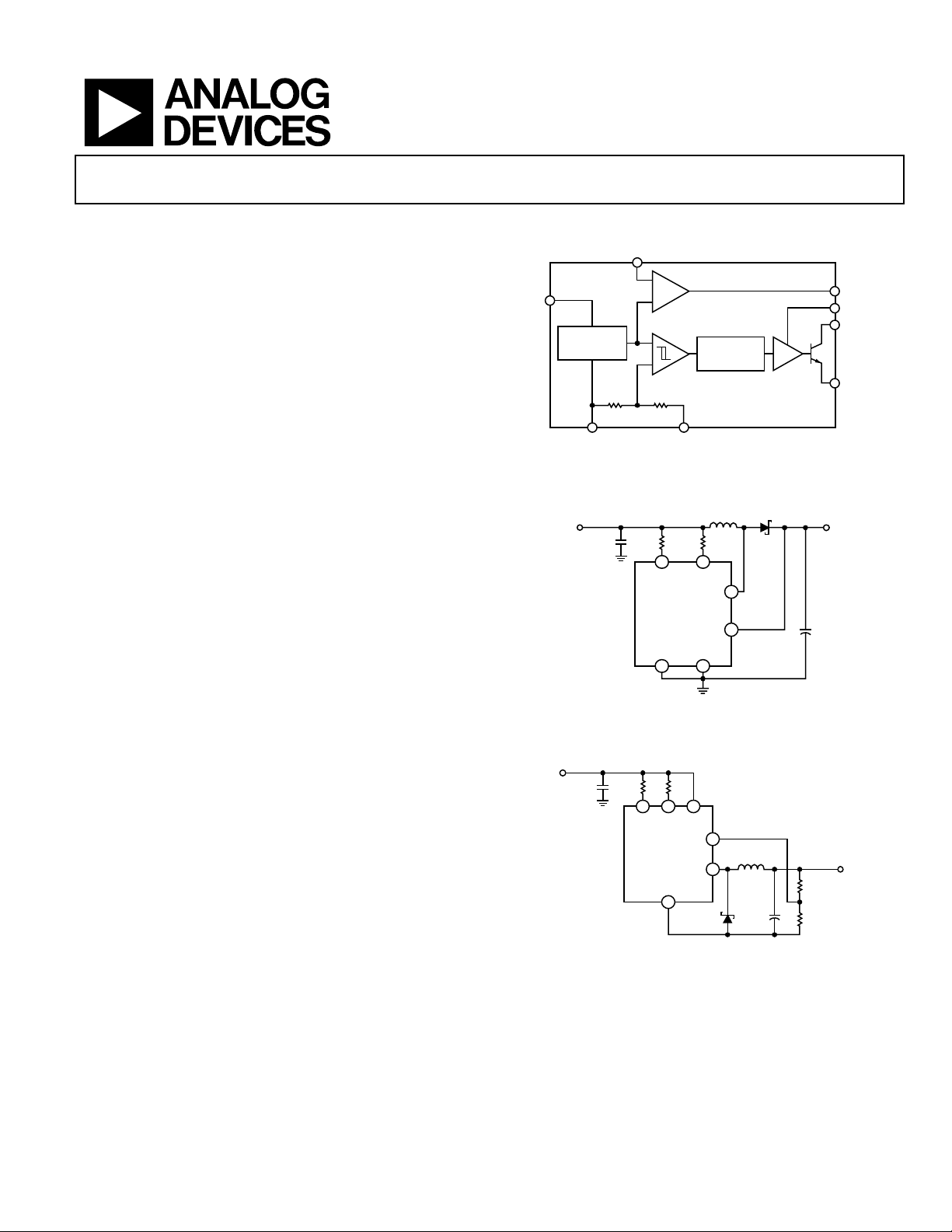
The auxiliary gain amplifier can be used as a low battery detector,
linear regulator, undervoltage lockout, or error amplifier.
FUNCTIONAL BLOCK DIAGRAMS
IN
1.245V
REFERENCE
R1 R2
GND SENSE
V
IN
2V TO 3.2V
5V TO 6V
100µF
10V
V
IN
C1
100µF
120Ω
10V
C1, C2 = AVX TPS D107 M010R0100
L1 = SUMIDA CR43-100
Figure 3. Step-Down Mode Operation
SET
A1
GAIN BLOCK/
ERROR AMP
400kHz
OSCILLATOR
COMPARATOR
Figure 1.
6.8µH
120V
2
1
I
V
LIM
IN
SW1
ADP3000-3.3V
FB
(SENSE)
SW2GND
4
5
C1, C2 = AVX TPS D107 M010R0100
L1 = SUMIDA CR43-6R8
Figure 2. Typical Application
R
LIM
SW1
3
8
FB
1 2
I
LIMVIN
ADP3000
4
SW2
GND
5
D1
1N5818
3
8
ADP3000
DRIVER
ADP3000
IN5817
+
L1
10µH
C
L
+
100µF
10V
C1
100µF
10V
R2
150kΩ
1%
R1
110kΩ
1%
A0
I
LIM
SW1
SW2
3.3V
180mA
V
OUT
3V
100mA
00122-001
00122-002
00122-003
Rev. A
Information furnished by Analog Devices is believed to be accurate and reliable.
However, no responsibility is assumed by Analog Devices for its use, nor for any
infringements of patents or other rights of third parties that may result from its use.
Specifications subject to change without notice. No license is granted by implication
or otherwise under any patent or patent rights of Analog Devices. Trademarks and
registered trademarks are the property of their respective owners.
One Technology Way, P.O. Box 9106, Norwood, MA 02062-9106, U.S.A.
Tel: 781.329.4700 www.analog.com
Fax: 781.326.8703 © 2004 Analog Devices, Inc. All rights reserved.

ADP3000
TABLE OF CONTENTS
Specifications..................................................................................... 3
Programming the Gain Block................................................... 11
Absolute Maximum Ratings............................................................ 4
ESD Caution.................................................................................. 4
Pin Configurations and Function Descriptions ........................... 5
Typical Performance Characteristics ............................................. 6
Theory of Operation ........................................................................ 9
Applications Information .............................................................. 10
Component Selection................................................................. 10
Programming the Switching Current Limit............................ 10
REVISION HISTORY
9/04—Data Sheet Changed from Rev. 0 to Rev. A
Added RU-14 Package .................................................Universal
Changes to Table 4.....................................................................10
Changes to Table 5.....................................................................10
Updated Outline Dimensions..................................................15
Changes to Ordering Guide.....................................................16
Power Transistor Protection Diode in Step-Down
Configuration ............................................................................. 11
Thermal Considerations............................................................ 11
Typical Application Circuits ......................................................... 13
Outline Dimensions....................................................................... 15
Ordering Guide .......................................................................... 16
1/97—Revision 0: Initial Version
Rev. A | Page 2 of 16

ADP3000
SPECIFICATIONS
0°C ≤ TA ≤ +70°C, VIN = 3 V, unless otherwise noted.1
Table 1.
ADP3000
Parameter Conditions Symbol Min Typ Max Unit
INPUT VOLTAGE Step-up mode V
Step-down mode 30.0 V
SHUT-DOWN QUIESCENT CURRENT VFB > 1.43 V; V
COMPARATOR TRIP POINT VOLTAGE ADP3000
2
OUTPUT SENSE VOLTAGE ADP3000-3.3
> 1.1 × V
SENSE
1.20 1.245 1.30 V
3
V
IQ 500 µA
OUT
ADP3000-53 4.75 5.00 5.25 V
ADP3000-123 11.40 12.00 12.60 V
COMPARATOR HYSTERESIS ADP3000 8 12.5 mV
OUTPUT HYSTERESIS ADP3000-3.3 32 50 mV
ADP3000-5 32 50 mV
ADP3000-12 75 120 mV
OSCILLATOR FREQUENCY f
DUTY CYCLE VFB < V
SWITCH-ON TIME I
LIM
D 65 80 %
REF
tied to VIN, VFB= 0 t
SWITCH SATURATION VOLTAGE TA = +25°C V
Step-Up Mode VIN = 3.0 V, ISW = 650 mA 0.5 0.75 V
V
= 5.0 V, ISW = 1 A 0.8 1.1 V
IN
Step-Down Mode VIN = 12 V, ISW = 650 mA 1.1 1.5 V
FEEDBACK PIN BIAS CURRENT ADP3000 VFB = 0 V I
SET PIN BIAS CURRENT V
GAIN BLOCK OUTPUT LOW I
REFERENCE LINE REGULATION
= V
SET
= 300 µA, V
SINK
5 V ≤ V
2 V ≤ V
I
REF
= 1.00 V V
SET
≤ 30 V
IN
≤ 5 V
IN
GAIN BLOCK GAIN RL = 100 kΩ4 A
GAIN BLOCK CURRENT SINK V
CURRENT LIMIT 220 Ω from I
≤ 1 V I
SET
to VIN I
LIM
CURRENT LIMIT TEMPERATURE COEFFICIENT
SWITCH-OFF LEAKAGE CURRENT Measured at SW1 pin 1 10 µA
V
= 12 V, TA = +25°C
SW1
MAXIMUM EXCURSION BELOW GND TA = +25°C
I
≤ 10 µA, switch off
SW1
2.0 12.6 V
IN
3.135 3.3 3.465 V
OUT
350 400 450 kHz
OSC
1.5 2 2.55 µs
ON
SAT
160 330 nA
FB
200 400 nA
SET
0.15 0.4 V
OL
0.02 0.15 %/V
0.2 0.6 %/V
1000 6000 V/V
V
300 µA
SINK
400 mA
LIM
−0.3
−400 −350
%/°C
mV
1
All limits at temperature extremes are guaranteed via correlation using standard statistical methods.
2
This specification guarantees that both the high and low trip points of the comparator fall within the 1.20 V to 1.30 V range.
3
The output voltage waveform will exhibit a saw-tooth shape due to the comparator hysteresis. The output voltage on the fixed output versions will always be within
the specified range.
4
100 kΩ resistor connected between a 5 V source and the AO pin.
Rev. A | Page 3 of 16

ADP3000
ABSOLUTE MAXIMUM RATINGS
Table 2.
Parameter Rating
Input Supply Voltage, Step-Up Mode 15 V
Input Supply Voltage, Step-Down Mode 36 V
SW1 Pin Voltage 50 V
SW2 Pin Voltage
Feedback Pin Voltage (ADP3000) 5.5 V
Switch Current 1.5 A
Maximum Power Dissipation 500 mW
Operating Temperature Range 0°C to +70°C
Storage Temperature Range
Lead Temperature (Soldering, 10 s) 300°C
Thermal Impedance
R-8 170°C/W
RU-14 150°C/W
N-8 120°C/W
ESD CAUTION
ESD (electrostatic discharge) sensitive device. Electrostatic charges as high as 4000 V readily
accumulate on the human body and test equipment and can discharge without detection. Although
this product features proprietary ESD protection circuitry, permanent damage may occur on devices
subjected to high energy electrostatic discharges. Therefore, proper ESD precautions are
recommended to avoid performance degradation or loss of functionality.
−0.5 V to V
−65°C to +150°C
IN
Stresses above those listed under Absolute Maximum Ratings
may cause permanent damage to the device. This is a stress
rating only; functional operation of the device at these or any
other conditions above those indicated in the operational
section of this specification is not implied. Exposure to
Absolute Maximum Rating conditions for extended periods
may affect device reliability.
Rev. A | Page 4 of 16

ADP3000
V
V
PIN CONFIGURATIONS AND FUNCTION DESCRIPTIONS
1
I
LIM
V
2
IN
SW1 3
SW2 4
*FIXED VERSIONS
ADP3000
TOP VIEW
(Not to Scale)
FB (SENSE)*8
SET7
6
AO
GND5
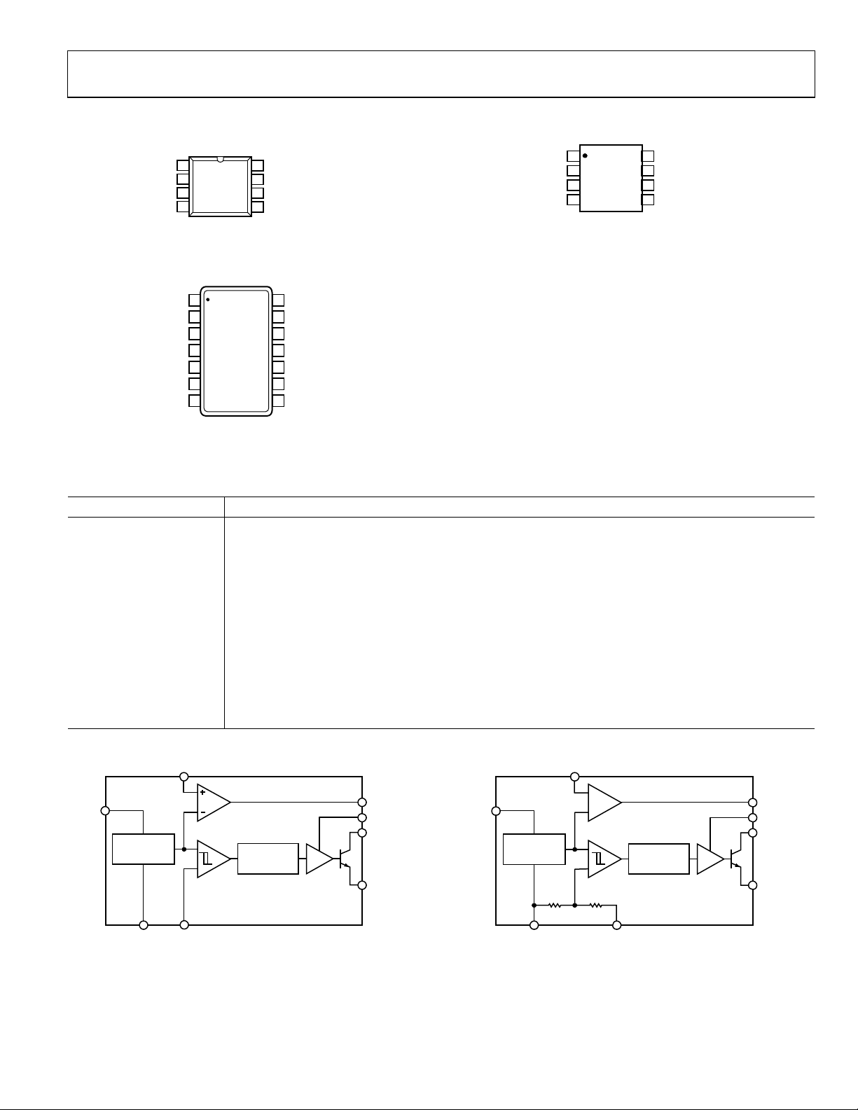
Figure 4. 8-Lead Plastic DIP (N-8)
1
NC
2
NC
3
ILIM
VIN
SW1
NC
SW2
ADP3000
4
TOP VIEW
(Not to Scale)
5
6
7
00122-004
14
NC
13
FB
12
SET
11
AO
NC
10
9
NC
8
GND
I
1
LIM
V
2
IN
ADP3000
SW1
3
TOP VIEW
(Not to Scale)
SW2
4
*FIXED VERSIONS
Figure 6. 8-Lead SOIC (R-8)
FB (SENSE)*
8
7
SET
6
AO
5
GND
00122-005
NC = NO CONNECT
00122-035
Figure 5. 14-lead TSSOP (RU-14)
Table 3. Pin Function Descriptions
Mnemonic Function
I
For normal conditions, connect to VIN. When lower current is required, connect a resistor between I
LIM
and VIN.
LIM
To limit the switch current to 400 mA, connect a 220 Ω resistor.
VIN
Input Voltage.
SW1 Collector of Power Transistor. For step-down configuration, connect to VIN. For step-up configuration, connect
to an inductor/diode.
SW2 Emitter of Power Transistor. For step-down configuration, connect to inductor/diode. For step-up
configuration, connect to ground. Do not allow pin to go more than a diode drop below ground.
GND Ground.
AO
Auxiliary Gain Block (GB) Output. Open collector can sink 300 µA. This pin can be left open if not used.
SET Auxiliary Gain Amplifier Input. The amplifier’s positive input is connected to the SET pin, and its negative
input is connected to the 1.245 V reference. This pin can be left open if not used.
FB/SENSE On the ADP3000 (adjustable) version, this pin is connected to the comparator input. On the ADP3000-3.3,
the ADP3000-5, and the ADP3000-12, the pin goes directly to the internal resistor divider that sets the
output voltage.
IN
1.245V
REFERENCE
SET
A2
A1
COMPARATOR
GAIN BLOCK/
ERROR AMP
OSCILLATOR
DRIVER
A0
I
LIM
SW1
SW2
IN
1.245V
REFERENCE
SET
A1
COMPARATOR
GAIN BLOCK/
ERROR AMP
OSCILLATOR
DRIVER
A0
I
LIM
SW1
SW2
ADP3000
GND
FB
Figure 7. Functional Block Diagram for Adjustable Version
00122-006
R1 R2
GND SENSE
ADP3000
Figure 8. Functional Block Diagram for Fixed Version
00122-007
Rev. A | Page 5 of 16
 Loading...