

Micropower Step-Up/Step-Down
COMPARATOR
GAIN BLOCK/
ERROR AMP
400kHz
OSCILLATOR
DRIVER
A1
1.245V
REFERENCE
R1 R2
ADP3000
SET
V
IN
GND SENSE
A0
I
LIM
SW1
SW2
ADP3000-3.3V
1 2
3
8
4
5
I
LIM
V
IN
SW1
FB
(SENSE)
SW2GND
+
100µF
10V
120Ω
6.8µH
IN5817
C1
100µF
10V
V
IN
2V–3.2V
3.3V @
180mA
C1, C2: AVX TPS D107 M010R0100
L1: SUMIDA CD43-6R8
Fixed 3.3 V, 5 V, 12 V and Adjustable
a
High Frequency Switching Regulator
FEATURES
Operates at Supply Voltages from 2 V to 30 V
Works in Step-Up or Step-Down Mode
Very Few External Components Required
High Frequency Operation Up to 400 kHz
Low Battery Detector on Chip
User Adjustable Current Limit
Fixed and Adjustable Output Voltage
8-Pin DIP and SO-8 Package
Small Inductors and Capacitors
APPLICATIONS
Notebook, Palmtop Computers
Cellular Telephones
Hard Disk Drives
Portable Instruments
Pagers
GENERAL DESCRIPTION
The ADP3000 is a versatile step-up/step-down switching
regulator that operates from an input supply voltage of 2 V to
12 V in step-up mode and up to 30 V in step-down mode.
The ADP3000 operates in Pulse Frequency Mode (PFM) and
consumes only 500 µA, making it highly suitable for applica-
tions that require low quiescent current.
The ADP3000 can deliver an output current of 100 mA at
3 V from a 5 V input in step-down configuration and 180 mA at
3.3 V from a 2 V input in step-up configuration.
The auxiliary gain amplifier can be used as a low battery detector,
linear regulator undervoltage lockout or error amplifier.
The ADP3000 operates at 400 kHz switching frequency. This
allows the use of small external components (inductors and
capacitors), making the device very suitable for space constrained
designs.
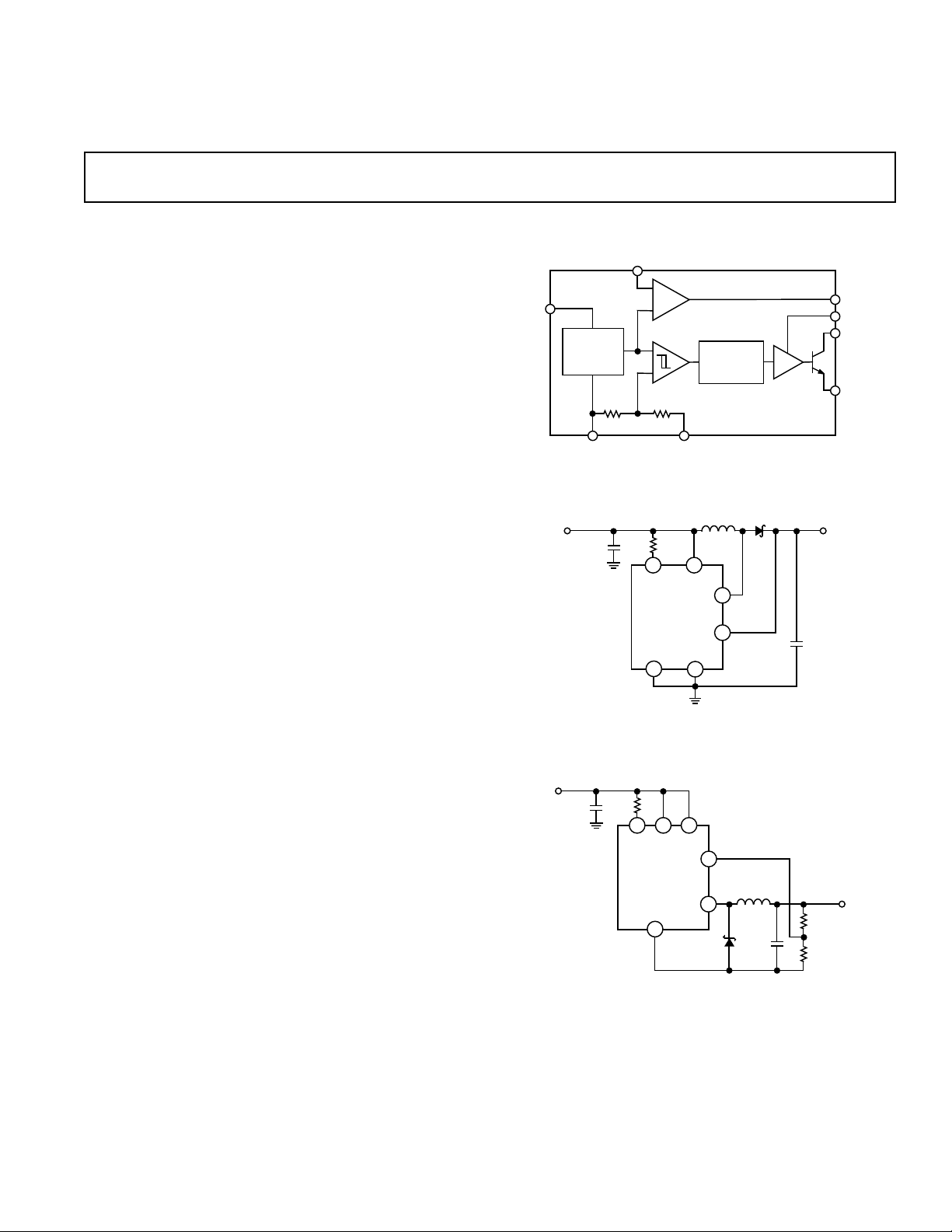
FUNCTIONAL BLOCK DIAGRAM
Figure 1. Typical Application
V
5V–6V
IN
100µF
R
C1
120Ω
10V
C1, C2: AVX TPS D107 M010R0100
L1: SUMIDA CD43-100
LIM
1 2 3
I
LIM
ADP3000
GND
ADP3000
V
SW1
IN
8
FB
L1
10µH
4
SW2
5
1N5818
D1
100µF
10V
CL
+
R2
150kΩ
1%
R1
110kΩ
1%
V
OUT
3V
100mA
REV. 0
Information furnished by Analog Devices is believed to be accurate and
reliable. However, no responsibility is assumed by Analog Devices for its
use, nor for any infringements of patents or other rights of third parties
which may result from its use. No license is granted by implication or
otherwise under any patent or patent rights of Analog Devices.
Figure 2. Step-Down Mode Operation
One Technology Way, P.O. Box 9106, Norwood, MA 02062-9106, U.S.A.
Tel: 617/329-4700 World Wide Web Site: http://www.analog.com
Fax: 617/326-8703 © Analog Devices, Inc., 1997

ADP3000–SPECIFICATIONS
(08C ≤ TA ≤ +708C, VIN = 3 V unless otherwise noted)*
ADP3000
Parameter Conditions Symbol Min Typ Max Units
INPUT VOLTAGE Step-Up Mode V
IN
2.0 12.6 V
Step-Down Mode 30.0 V
SHUTDOWN QUIESCENT CURRENT V
COMPARATOR TRIP POINT ADP3000
> 1.43 V; V
FB
> 1.1 × V
SENSE
1
OUTIQ
1.20 1.245 1.30 V
500 µA
VOLTAGE
OUTPUT SENSE VOLTAGE ADP3000-3.3
ADP3000-5
ADP3000-12
2
2
2
V
OUT
3.135 3.3 3.465 V
4.75 5.00 5.25 V
11.40 12.00 12.60 V
COMPARATOR HYSTERESIS ADP3000 8 12.5 mV
OUTPUT HYSTERESIS ADP3000-3.3 32 50 mV
ADP3000-5 32 50 mV
ADP3000-12 75 120 mV
OSCILLATOR FREQUENCY f
DUTY CYCLE V
SWITCH ON TIME I
SWITCH SATURATION VOLTAGE T
STEP-UP MODE V
> V
FB
REF
Tied to VIN, VFB = 0 t
LIM
= +25°C
A
= 3.0 V, ISW = 650 mA V
IN
V
= 5.0 V, ISW = 1 A 0.8 1.1 V
IN
OSC
D6580 %
ON
SAT
350 400 450 kHz
1.5 2 2.55 µs
0.5 0.75 V
STEP-DOWN MODE VIN = 12 V, ISW = 650 mA 1.1 1.5 V
FEEDBACK PIN BIAS CURRENT ADP3000 VFB = 0 V I
SET PIN BIAS CURRENT V
GAIN BLOCK OUTPUT LOW I
REFERENCE LINE REGULATION 5 V ≤ V
= V
SET
REF
= 300 µAV
SINK
V
= 1.00 V
SET
≤ 30 V 0.02 0.15 %/V
IN
I
FB
SET
OL
160 330 nA
200 400 nA
0.15 0.4 V
2 V ≤ VIN ≤ 5 V 0.2 0.6 %/V
GAIN BLOCK GAIN R
GAIN BLOCK CURRENT SINK V
= 100 kΩ
L
≤ 1 V I
SET
CURRENT LIMIT 220 Ω from I
3
LIM
to V
A
V
SINK
IN
I
LIM
1000 6000 V/V
300 µA
400 mA
CURRENT LIMIT TEMPERATURE
COEFFICIENT –0.3 %/°C
SWITCH OFF LEAKAGE CURRENT Measured at SW1 Pin 1 10 µA
V
= 12 V, T
SW1
MAXIMUM EXCURSION BELOW GND T
NOTES
1
This specification guarantees that both the high and low trip point of the comparator fall within the 1.20 V to 1.30 V range.
2
The output voltage waveform will exhibit a sawtooth shape due to the comparator hysteresis. The output voltage on the fixed output versions will always be within the
specified range.
3
100 kΩ resistor connected between a 5 V source and the AO pin.
*All limits at temperature extremes are guaranteed via correlation using standard statistical methods.
Specifications subject to change without notice.
= +25°C
A
I
≤ 10 µA, Switch Off –400 –350 mV
SW1
= +25°C
A
–2–
REV. 0
ADP3000
WARNING!
ESD SENSITIVE DEVICE
1
2
3
4
8
7
6
5
TOP VIEW
(Not to Scale)
ADP3000
I
LIM
V
IN
SW1
SW2
FB (SENSE)*
SET
AO
GND
* FIXED VERSIONS
1
2
3
4
8
7
6
5
TOP VIEW
(Not to Scale)
ADP3000
I
LIM
V
IN
SW1
SW2
FB (SENSE)*
SET
AO
GND
* FIXED VERSIONS
PIN DESCRIPTIONS
Mnemonic Function
I
LIM
For normal conditions this pin is connected to
V
. When lower current is required, a resistor
IN
should be connected between I
LIM
and V
IN.
Limiting the switch current to 400 mA is
achieved by connecting a 220 Ω resistor.
V
IN
Input Voltage.
SW1 Collector of power transistor. For step-down
configuration, connect to V
For step-up
IN.
configuration, connect to an inductor/diode.
SW2 Emitter of power transistor. For step-down
configuration, connect to inductor/diode.
For step-up configuration, connect to ground.
Do not allow this pin to go more than a diode
drop below ground.
GND Ground.
AO Auxiliary Gain (GB) output. The open col-
lector can sink 300 µA. It can be left open
if not used.
SET SET Gain amplifier input. The amplifier’s
positive input is connected to SET pin and its
negative input is connected to 1.245 V. It can
be left open if not used.
FB/SENSE On the ADP3000 (adjustable) version, this pin
is connected to the comparator input. On the
ADP3000-3.3, ADP3000-5 and ADP3000-12,
the pin goes directly to the internal resistor
divider that sets the output voltage.
ABSOLUTE MAXIMUM RATINGS
Input Supply Voltage, Step-Up Mode . . . . . . . . . . . . . . . 15 V
Input Supply Voltage, Step-Down Mode . . . . . . . . . . . . . 36 V
SW1 Pin Voltage . . . . . . . . . . . . . . . . . . . . . . . . . . . . . . . 50 V
SW2 Pin Voltage . . . . . . . . . . . . . . . . . . . . . . . . –0.5 V to V
Feedback Pin Voltage (ADP3000) . . . . . . . . . . . . . . . . . .5.5 V
Switch Current . . . . . . . . . . . . . . . . . . . . . . . . . . . . . . . .1.5 A
Maximum Power Dissipation . . . . . . . . . . . . . . . . . . 500 mW
Operating Temperature Range . . . . . . . . . . . . . 0°C to +70°C
Storage Temperature Range . . . . . . . . . . . . –65°C to +150°C
Lead Temperature (Soldering, 10 sec) . . . . . . . . . . . .+300°C
Thermal Impedance
SO-8 . . . . . . . . . . . . . . . . . . . . . . . . . . . . . . . . . . 170°C/W
N-8 . . . . . . . . . . . . . . . . . . . . . . . . . . . . . . . . . . . 120°C/W
PIN CONFIGURATIONS
8-Lead Plastic DIP 8-Lead SOIC
(N-8) (SO-8)
ORDERING GUIDE
Output Package
Model Voltage Option
ADP3000AN-3.3 3.3 V N-8
ADP3000AR-3.3 3.3 V SO-8
ADP3000AN-5 5 V N-8
ADP3000AR-5 5 V SO-8
ADP3000AN-12 12 V N-8
ADP3000AR-12 12 V SO-8
ADP3000AN Adjustable N-8
ADP3000AR Adjustable SO-8
N = plastic DIP, SO = small outline package.
IN
SET
V
IN
1.245V
REFERENCE
A2
GAIN BLOCK/
ERROR AMP
A1
COMPARATOR
OSCILLATOR
DRIVER
A0
I
LIM
SW1
SW2
ADP3000
GND FB
Figure 3a. Functional Block Diagram for Adjustable Version
V
IN
1.245V
REFERENCE
Figure 3b. Functional Block Diagram for Fixed Version
SET
A1
GAIN BLOCK/
ERROR AMP
COMPARATOR
R1 R2
GND SENSE
CAUTION
ESD (electrostatic discharge) sensitive device. Electrostatic charges as high as 4000 V readily
accumulate on the human body and test equipment and can discharge without detection.
Although the ADP3000 features proprietary ESD protection circuitry, permanent damage may
occur on devices subjected to high energy electrostatic discharges. Therefore, proper ESD
precautions are recommended to avoid performance degradation or loss of functionality.
REV. 0
–3–
OSCILLATOR
ADP3000
DRIVER
A0
I
LIM
SW1
SW2
ADP3000
INPUT VOLTAGE – V
1400
0
1.5 3 30
6 9 12 15 18 21 24 27
1200
1000
800
600
400
200
QUIESCENT CURRENT – µA
QUIESCENT CURRENT @ TA = +25°C
R
LIM
– Ω
SWITCH CURRENT – A
1.8
1.6
0
110 1k
100
0.6
0.2
0.4
1.0
0.8
1.4
1.2
TA = +25°C
TA = +85°C
TA = 0°C
VIN = 12V
–Typical Characteristics
2.5
2.0
1.5
1.0
ON VOLTAGE – V
0.5
0
0.1 0.2 1.5
VIN = 5V @ TA = +25°C
VIN = 3V @ TA = +25°C
VIN = 2V @ TA = +25°C
0.4 0.6 0.8 1.0 1.2 1.4
SWITCH CURRENT – A
Figure 4. Switch ON Voltage vs.
Switch Current in Step-Up Mode
406
OSCILLATOR FREQUENCY –
= +25°C
@ T
405
A
404
403
402
401
400
OSCILLATOR FREQUENCY – kHz
399
396
24 306 8 10 12 15 18 21 24 27
INPUT VOLTAGE – V
1.4
VIN = 5V @ TA = +25°C
1.2
1.0
0.8
– V
0.6
CE(SAT)
V
0.4
0.2
0.0
0.1
0.2
VIN = 12V @ TA = +25°C
0.3 0.4 0.5 0.6
SWITCH CURRENT – A
0.8
0.9
Figure 5. Saturation Voltage vs.
Switch Current in Step-Down Mode
0.8
VIN = 5V
0.7
0.6
0.5
0.4
0.3
0.2
SWITCH CURRENT – A
0.1
0
110 1k
TA = +25°C
R
– Ω
LIM
TA = +85°C
TA = 0°C
100
Figure 6. Quiescent Current vs.
Input Voltage
Figure 7. Oscillator Frequency vs.
Input Voltage
1.8
VIN = 3V
1.6
1.4
– Ω
TA = 0°C
100
1.2
TA = +25°C
1.0
0.8
0.6
SWITCH CURRENT – A
0.4
0.2
0
110 1k
Figure 8c. Maximum Switch Current
vs. R
LIM
TA = +85°C
R
LIM
in Step-Up Mode (3 V)
Figure 8a. Maximum Switch Current
vs. R
in Step-Down Mode (5 V)
LIM
440
430
420
410
400
390
380
370
360
350
OSCILLATOR FREQUENCY – kHz
340
330
–40 0 85
TEMPERATURE – °C (TA)
25 70
Figure 9. Oscillator Frequency vs.
Temperature
–4–
Figure 8b. Maximum Switch Current
vs. R
in Step-Down Mode (12 V)
LIM
2.30
2.25
2.20
2.15
2.10
2.05
2.00
ON TIME – µs
1.95
1.90
1.85
1.80
–40 0 85
TEMPERATURE – °C (TA)
25 70
Figure 10. Switch ON Time vs.
Temperature
REV. 0

ADP3000
TEMPERATURE – °C (TA)
ON VOLTAGE – V
1.25
1.20
0.90
–40 0 8525 70
1.10
1.05
1.00
0.95
1.15
VIN = 12V @ ISW = 0.65A
100
90
80
70
60
50
40
DUTY CYCLE – %
30
20
10
0
–40 0 85
TEMPERATURE – °C (TA)
25 70
Figure 11. Duty Cycle vs.
Temperature
250
200
150
100
BIAS CURRENT – µA
50
0
–40 0 85
TEMPERATURE – °C (TA)
25 70
0.56
0.54
0.52
0.50
0.48
0.46
SATURATION VOLTAGE – V
0.44
0.42
–40 0 85
VIN = 3V @ ISW = 0.65A
25 70
TEMPERATURE – °C (TA)
Figure 12. Saturation Voltage vs.
Temperature in Step-Up Mode
700
VIN = 20V
600
500
400
300
200
QUIESCENT CURRENT – µA
100
0
–40 0 8525 70
TEMPERATURE – °C (TA)
Figure 13. Switch ON Voltage vs.
Temperature in Step-Down Mode
350
300
250
200
150
100
BIAS CURRENT – µA
50
0
–40 0 8525 70
TEMPERATURE – °C (TA)
Figure 14. Feedback Bias Current
vs. Temperature
Figure 15. Quiescent Current vs.
Temperature
Figure 16. Set Pin Bias Current vs.
Temperature
REV. 0
–5–

ADP3000
THEORY OF OPERATION
The ADP3000 is a versatile, high frequency, switch mode
power supply (SMPS) controller. The regulated output
voltage can be greater than the input voltage (boost or step-up
mode) or less than the input (buck or step-down mode). This
device uses a gated oscillator technique to provide high performance with low quiescent current.
A functional block diagram of the ADP3000 is shown in
Figure 3a. The internal 1.245 V reference is connected to one
input of the comparator, while the other input is externally
connected (via the FB pin) to a resistor divider connected to
the regulated output. When the voltage at the FB pin falls below
1.245 V, the 400 kHz oscillator turns on. A driver amplifier
provides base drive to the internal power switch and the switching
action raises the output voltage. When the voltage at the FB
pin exceeds 1.245 V, the oscillator is shut off. While the
oscillator is off, the ADP3000 quiescent current is only 500 µA.
The comparator’s hysteresis ensures loop stability without
requiring external components for frequency compensation.
The maximum current in the internal power switch can be set
by connecting a resistor between V
and the I
IN
pin. When
LIM
the maximum current is exceeded, the switch is turned OFF.
The current limit circuitry has a time delay of about 0.3 µs. If
an external resistor is not used, connect I
to VIN. This
LIM
yields the maximum feasible current limit. Further information
on I
is included in the “Applications” section of this data
LIM
sheet. The ADP3000 internal oscillator provides typically 1.7
µs ON and 0.8 µs OFF times.
An uncommitted gain block on the ADP3000 can be connected as a low battery detector. The inverting input of the
gain block is internally connected to the 1.245 V reference.
The noninverting input is available at the SET pin. A resistor
divider, connected between V
and GND with the junction
IN
connected to the SET pin, causes the AO output to go LOW
when the low battery set point is exceeded. The AO output is
an open collector NPN transistor that can sink in excess of
300 µA.
The ADP3000 provides external connections for both the
collector and emitter of its internal power switch, which permits
both step-up and step-down modes of operation. For the stepup mode, the emitter (Pin SW2) is connected to GND and the
collector (Pin SW1) drives the inductor. For step-down mode,
the emitter drives the inductor while the collector is connected
to V
.
IN
The output voltage of the ADP3000 is set with two external
resistors. Three fixed voltage models are also available:
ADP3000–3.3 (+3.3 V), ADP3000–5 (+5 V) and ADP3000–12
(+12 V). The fixed voltage models include laser-trimmed
voltage-setting resistors on the chip. On the fixed voltage models
of the ADP3000, simply connect the feedback pin (Pin 8)
directly to the output voltage.
APPLICATIONS INFORMATION
COMPONENT SELECTION
Inductor Selection
For most applications the inductor used with the ADP3000 will
fall in the range between 4.7 µH to 33 µH. Table I shows
recommended inductors and their vendors.
When selecting an inductor, it is very important to make sure
that the inductor used with the ADP3000 is able to handle a
current that is higher than the ADP3000’s current limit without
saturation.
As a rule of thumb, powdered iron cores saturate softly, whereas
Ferrite cores saturate abruptly. Rod or “open” drum core
geometry inductors saturate gradually. Inductors that saturate
gradually are easier to use. Even though rod or drum core
inductors are attractive in both price and physical size, these
types of inductors must be handled with care because they have
high magnetic radiation. Toroid or “closed” core geometry
should be used when minimizing EMI is critical.
In addition, inductor dc resistance causes power loss. It is best
to use low dc resistance inductors so that power loss in the
inductor is kept to the minimum. Typically, it is best to use an
inductor with a dc resistance lower than 0.2 Ω.
Table I. Recommended Inductors
V
endor Series Core Type Phone Numbers
Coiltronics OCTAPAC Toroid (407) 241-7876
Coiltronics UNIPAC Open (407) 241-7876
Sumida CD43, CD54 Open (847) 956-0666
Sumida CDRH62, CDRH73, Semi-Closed (847) 956-0666
CDRH64 Geometry
Capacitor Selection
For most applications, the capacitor used with the ADP3000
will fall in the range between 33 µF to 220 µF. Table II shows
recommended capacitors and their vendors.
For input and output capacitors, use low ESR type capacitors
for best efficiency and lowest ripple. Recommended capacitors
include AVX TPS series, Sprague 595D series, Panasonic HFQ
series and Sanyo OS-CON series.
When selecting a capacitor, it is important to make sure the
maximum capacitor ripple current rms rating is higher than the
ADP3000’s rms switching current.
It is best to protect the input capacitor from high turn-on current charging surges by derating the capacitor voltage by 2:1.
For very low input or output voltage ripple requirements,
Sanyo OS-CON series capacitors can be used since this type of
capacitor has very low ESR. Alternatively, two or more tantalum capacitors can be used in parallel.
–6–
REV. 0

ADP3000
ADP3000
1.245V
REF
GND
AO
5V
R
L
47kΩ
TO
PROCESSOR
R1
V
BATT
V
IN
SET
R
HYS
R2
33kΩ
1.6MΩ
V
LB
= BATTERY TRIP POINT
R1 =
V
LB
– 1.245V
37.7µA
Table II. Recommended Capacitors
Vendor Series Type Phone Numbers
AVX TPS Surface Mount (803) 448-9411
Sanyo OS-CON Through-Hole (619) 661-6835
Sprague 595D Surface Mount (603) 224-1961
Panasonic HFQ Through-Hole (201) 348-5200
DIODE SELECTION
The ADP3000’s high switching speed demands the use of
Schottky diodes. Suitable choices include the 1N5817, 1N5818,
1N5819, MBRS120LT3 and MBR0520LT1. Do not use fast
recovery diodes because their high forward drop lowers efficiency. Neither general-purpose diodes nor small signal diodes
should be used.
PROGRAMMING THE SWITCHING CURRENT LIMIT
OF THE POWER SWITCH
The ADP3000’s R
pin permits the cycle by cycle switch
LIM
current limit to be programmed with a single external resistor.
This feature offers major advantages which ultimately decrease
the component cost and P.C.B. real estate. First, it allows the
ADP3000 to use low value, low saturation current and physically small inductors. Additionally, it allows the ADP3000 to
use a physically small surface mount tantalum capacitor with a
typical ESR of 0.1 Ω to achieve an output ripple as low as 40
mV to 80 mV, as well as low input ripple.
As a rule of thumb, the current limit is usually set to approximately
3 to 5 times the full load current for boost applications and
about 1.5–3 times of the full load current in buck applications.
The internal structure of the I
circuit is shown in Figure 17.
LIM
Q1 is the ADP3000’s internal power switch, which is paralleled
by sense transistor Q2. The relative sizes of Q1 and Q2 are
scaled so that IQ2 is 0.5% of IQ1. Current flows to Q2 through
both an internal 80 Ω resistor and the R
resistor. The voltage
LIM
on these two resistors biases the base-emitter junction of the
oscillator-disable transistor, Q3. When the voltage across R1
and R
pulse. If only the 80 Ω internal resistor is used (i.e. the I
is connected directly to V
exceeds 0.6 V, Q3 turns on and terminates the output
LIM
), the maximum switch current will
IN
LIM
pin
be 1.5 A. Figure 8a gives values for lower current-limit values.
The delay through the current limiting circuit is approximately
0.3 µs. If the switch ON time is reduced to less than 1.7 µs,
accuracy of the current trip-point is reduced. Attempting to
program a switch ON time of 0.3 µs or less will produce
spurious responses in the switch ON time. However, the
ADP3000 will still provide a properly regulated output voltage.
PROGRAMMING THE GAIN BLOCK
The gain block of the ADP3000 can be used as a low battery
detector, error amplifier or linear post regulator. The gain block
consists of an op amp with PNP inputs and an open-collector
NPN output. The inverting input is internally connected to the
ADP3000’s 1.245 V reference, while the noninverting input is
available at the SET pin. The NPN output transistor will sink in
excess of 300 µA.
Figure 18 shows the gain block configured as a low battery
monitor. Resistors R1 and R2 should be set to high values to
reduce quiescent current, but not so high that bias current in
the SET input causes large errors. A value of 33 kΩ for R2 is a
good compromise. The value for R1 is then calculated from the
formula:
LOBATT
1.245 V
–1.245 V
R2
where V
V
R1=
is the desired low battery trip point. Since the
LOBATT
gain block output is an open-collector NPN, a pull-up resistor
should be connected to the positive logic power supply.
REV. 0
R
LIM
V
IN
ADP3000
Figure 17. ADP3000 Current Limit Operation
V
IN
Q3
400kHz
OSC
(EXTERNAL)
I
R1
DRIVER
LIM
80Ω
(INTERNAL)
I
Q1
SW1
200
Q2
SW2
Q1
POWER
SWITCH
Figure 18. Setting the Low Battery Detector Trip Point
–7–

ADP3000
PD= 0.82×1+
(2)(0.8)
30
0.75
[]
1–
2
3.3
(4)0.18
0.8
+ 500E −6
[]
2
[]
The circuit of Figure 18 may produce multiple pulses when
approaching the trip point due to noise coupled into the SET
input. To prevent multiple interrupts to the digital logic,
hysteresis can be added to the circuit (Figure 18). Resistor R
HYS
,
with a value of 1 MΩ to 10 MΩ, provides the hysteresis. The
addition of R
will change the trip point slightly, so the new
HYS
value for R1 will be:
R1=
V
1.245V
R2
LOBATT
−
–1.245V
V
−1.245V
L
R
L+RHYS
where VL is the logic power supply voltage, RL is the pull-up
resistor, and R
creates the hysteresis.
HYS
POWER TRANSISTOR PROTECTION DIODE IN STEPDOWN CONFIGURATION
When operating the ADP3000 in the step-down mode, the
output voltage is impressed across the internal power switch’s
emitter-base junction when the switch is off. In order to protect
the switch, a Schottky diode must be placed in a series with
SW2 when the output voltage is set to higher than 6 V. Figure
19 shows the proper way to place the protection diode, D2.
The selection of this diode is identical to the step-down commuting diode (see Diode Selection section for information).
V
IN
+
R3
C2
1 2 3
I
LIM
ADP3000
GND
D1, D2 = 1N5818 SCHOTTKY DIODES
VINSW1
5
SW2
8
FB
D2
4
D1
V
> 6V
OUT
L1
R2
+
R1
C1
Step-Down
PD= ISWV
where: ISW is I
1
1+
CESAT
in the case of current limit is programmed
LIMIT
VIN– V
β
V
O
CE SAT
()
2I
O
I
SW
+ I
V
[]
[]
Q
IN
externally or maximum inductor current in the case of
current limit is not programmed eternally.
V
= Check this value by applying ISW to Figure 8b.
CE(SAT)
1.2 V is typical value.
D = 0.75 (Typical Duty Ratio for a Single Switching
Cycle).
V
= Output Voltage.
O
= Output Current.
I
O
= Input Voltage.
V
IN
= 500 µA (Typical Shutdown Quiescent Current).
I
Q
β = 30 (Typical Forced Beta).
The temperature rise can be calculated from:
where:
∆T = PD×θ
JA
∆T = Temperature Rise.
= Device Power Dissipation.
P
D
= Thermal Resistance (Junction-to-Ambient).
θ
JA
As example, consider a boost converter with the following
specifications:
VIN = 2 V, IO = 180 mA, VO = 3.3 V.
I
= 0.8 A (Externally Programmed).
SW
With Step-Up Power Dissipation Equation:
Figure 19. Step-Down Model V
OUT
> 6.0 V
THERMAL CONSIDERATIONS
Power dissipation internal to the ADP3000 can be approximated
with the following equations.
Step-Up
PD= I
where: ISW is I
INISW
β
D 1–
V
2
R +
SW
in the case of current limit programmed
LIMIT
V
IN
V
O
4I
O
+ I
V
[]
[]
Q
I
SW
IN
externally, or maximum inductor current in the case of
current limit not programmed externally.
R = 1 Ω (Typical R
CE(SAT)
).
D = 0.75 (Typical Duty Ratio for a Single Switching
Cycle).
VO = Output Voltage.
= Output Current.
I
O
= Input Voltage.
V
IN
= 500 µA (Typical Shutdown Quiescent Current).
I
Q
β = 30 (Typical Forced Beta)
= 185 mW
Using the SO-8 Package: ∆T = 185 mW (170°C/W) = 31.5°C.
Using the N-8 Package: ∆T = 185 mW (120°C/W) = 22.2°C.
At a 70°C ambient, die temperature would be 101.45°C for
SO-8 package and 92.2°C for N-8 package. These junction
temperatures are well below the maximum recommended
junction temperature of 125°C.
Finally, the die temperature can be decreased up to 20% by
using a large metal ground plate as ground pickup for the
ADP3000.
–8–
REV. 0

Typical Application Circuits
I
LIM V
IN
SW1
SW2
SENSE
GND
ADP3000-12V
L1
15µH
124Ω
8
1
2
45
3
1N5817
C1
100µF
10V
+
C2
100µF
16V
+
V
IN
4.5V → 5.5V
V
OUT
12V
50mA
L1 = SUMIDA CD54-150
C1 = AVX TPS D107 M010R0100
C2 = AVX TPS E107 M016R0100
TYPICAL EFFICIENCY = 75%
I
LIM
VINSW1
FB
SW2
GND
ADP3000-ADJ
C1
100µF
10V
V
IN
5V → 6V
4
1 2 3
8
5
+
L1
10µH
V
OUT
3V
100mA
+
D1
IN5817
R2
150kΩ
R1
110kΩ
C2
100µF
10V
120Ω
L1 = SUMIDA CD43-100
C1, C2 = AVX TPS D107 M010R100
TYPICAL EFFICIENCY = 75%
L1
1
GND
120Ω
6.8µH
2
IN
SW1
SENSE
SW2
45
3
8
V
IN
2V → 3.2V
+
C1
100µF
10V
I
ADP3000-3.3V
L1 = SUMIDA CD43-6R8
C1, C2 = AVX TPS D107 M010R100
TYPICAL EFFICIENCY = 75%
LIM V
1N5817
ADP3000
V
OUT
3.3V
180mA
+
C2
100µF
10V
Figure 20. 2 V to 3.3 V/180 mA Step-Up Converter
L1
6.8µH
SW1
45
3
8
1N5817
V
OUT
5V
100mA
+
C2
100µF
10V
V
IN
2V → 3.2V
+
C1
100µF
10V
120Ω
1
I
LIM
ADP3000-5V
GND
L1 = SUMIDA CD43-6R8
C1, C2 = AVX TPS D107 M010R0100
TYPICAL EFFICIENCY = 80%
2
V
IN
SENSE
SW2
Figure 21. 2 V to 5 V/100 mA Step-Up Converter
L1
6.8µH
SW1
3
8
1N5817
V
OUT
5V
150mA
+
C2
100µF
10V
V
IN
2.7V → 4.5V
+
C1
100µF
10V
1
I
LIM
ADP3000-5V
GND
L1 = SUMIDA CD43-6R8
C1, C2 = AVX TPS D107 M010R100
TYPICAL EFFICIENCY = 80%
120Ω
2
V
IN
SENSE
SW2
45
Figure 23. 4.5 V to 12 V/ 50 mA Step-Up Converter
Figure 24. 5 V to 3 V/100 mA Step-Down Converter
V
IN
10V → 13V
L1 = SUMIDA CD43-100
C1 = AVX TPS D336 M020R0200
C2 = AVX TPS D107 M010R0100
TYPICAL EFFICIENCY = 77%
33µF
20V
+
C1
250Ω
1 2 3
I
VINSW1
LIM
SENSE
8
ADP3000-5V
SW2
GND
5
IN5817
L1
10µH
4
D1
V
OUT
5V
250mA
C2
+
100µF
10V
Figure 22. 2.7 V to 5 V/150 mA Step-Up Converter
REV. 0
Figure 25. 10 V to 5 V/250 mA Step-Down Converter
–9–

ADP3000
V
IN
+
5V
C1
240Ω
47µF
16V
1 2 3
I
VINSW1
LIM
SENSE
8
ADP3000-5V
4
SW2
GND
L1 = SUMIDA CD53-150
C1 = AVX TPS D476 M016R0150
C2 = AVX TPS D107 M010R0100
TYPICAL EFFICIENCY = 60%
5
IN5817
D1
Figure 26. 5 V to –5 V/100 mA Inverter
L1
15µH
100µF
10V
+
C2
V
OUT
–5V
100mA
2.5V → 4.2V
(SUMIDA – CDRH62)
330kΩ
2N2907
100kΩ
33nF
FB
10kΩ
90kΩ
6.8µH
IN5817
348kΩ
200kΩ
1%
1%
100µF
+
10V
–
AVX-TPS
IN1
IN2
ADP3302AR1
SD
GND
+
–
100kΩ
100µF
10V
AVX-TPS
90kΩ
1MΩ
120Ω
I
SET
ADP3000
A
O
GND SW2
LIMVIN
SW1
Figure 27. 1 Cell LI-ION to 3 V/200 mA Converter with Shutdown at VIN ≤ 2.5 V
AT V
≤ 2.5V
80
75
70
% EFFICIENCY
65
2.6 3.0 3.4 3.8 4.2
= 50mA + 50mA
I
O
I
O
= 100mA + 100mA
IN
SHDN IQ = 500µA
V
IN
(V)
Figure 28. Typical Efficiency of the Circuit of Figure 27
V
O1
V
O2
1µF
6V
(MLC)
1µF
6V
(MLC)
3V
100mA
3V
100mA
–10–
REV. 0

OUTLINE DIMENSIONS
Dimensions shown in inches and (mm).
8-Lead Plastic DIP 8-Lead SOIC
(N-8) (SO-8)
ADP3000
0.210 (5.33)
MAX
0.160 (4.06)
0.115 (2.93)
0.022 (0.558)
0.014 (0.356)
0.430 (10.92)
0.348 (8.84)
8
14
PIN 1
0.100
(2.54)
BSC
5
0.280 (7.11)
0.240 (6.10)
0.060 (1.52)
0.015 (0.38)
0.070 (1.77)
0.045 (1.15)
0.130
(3.30)
MIN
SEATING
PLANE
0.325 (8.25)
0.300 (7.62)
0.015 (0.381)
0.008 (0.204)
0.195 (4.95)
0.115 (2.93)
0.1574 (4.00)
0.1497 (3.80)
PIN 1
0.0098 (0.25)
0.0040 (0.10)
SEATING
PLANE
0.1968 (5.00)
0.1890 (4.80)
8
0.0688 (1.75)
0.0532 (1.35)
0.0500
0.0192 (0.49)
(1.27)
0.0138 (0.35)
BSC
5
0.2440 (6.20)
41
0.2284 (5.80)
0.0098 (0.25)
0.0075 (0.19)
0.0196 (0.50)
0.0099 (0.25)
8°
0°
0.0500 (1.27)
0.0160 (0.41)
x 45°
REV. 0
–11–

C2223–12–1/97
–12–
PRINTED IN U.S.A.
 Loading...