Step-Down DC-to-DC Regulator
ADP2441
Rev. 0
Information furnished by Analog Devices is believed to be accurate and reliable. However, no
Trademarks and registered trademarks are the property of their respective owners.
Fax: 781.461.3113 ©2012 Analog Devices, Inc. All rights reserved.
FB
COMP
EN
PGOOD
FREQ
SS/TRK
PGND
VIN
SW
BST
AGND
VCC
ADP2441
C4
C3
C
BST
C
IN
C
OUT
R
TOP
R
FREQ
R
COMP
C
COMP
R
BOTTOM
V
OUT
10581-001
V
OUT
V
IN
0
20
40
60
80
100
10
30
50
70
90
0.02 0.2 1
EFFICIENCY (%)
LOAD (A)
V
OUT
= 3.3V
10581-002
V
OUT
= 5V
V
OUT
= 12V
V
IN
= 24V
f
SW
= 300kHz
Data Sheet
FEATURES
Wide input voltage range of 4.5 V to 36 V
Low minimum on time of 50 ns
Maximum load current of 1 A
High efficiency of up to 94%
Adjustable output down to 0.6 V
±1% output voltage accuracy
Adjustable switching frequency of 300 kHz to 1 MHz
Pulse skip mode at light load for power saving
Precision enable input pin
Open-drain power good
External soft start with tracking
Overcurrent-limit protection
Shutdown current of less than 15 µA
UVLO and thermal shutdown
12-lead, 3 mm × 3 mm LFCSP package
APPLICAT ION S
Point of load applications
Distributed power systems
Industrial control supplies
Standard rail conversion to 24 V/12 V/5 V/3.3 V
36 V,1 A, Synchronous,
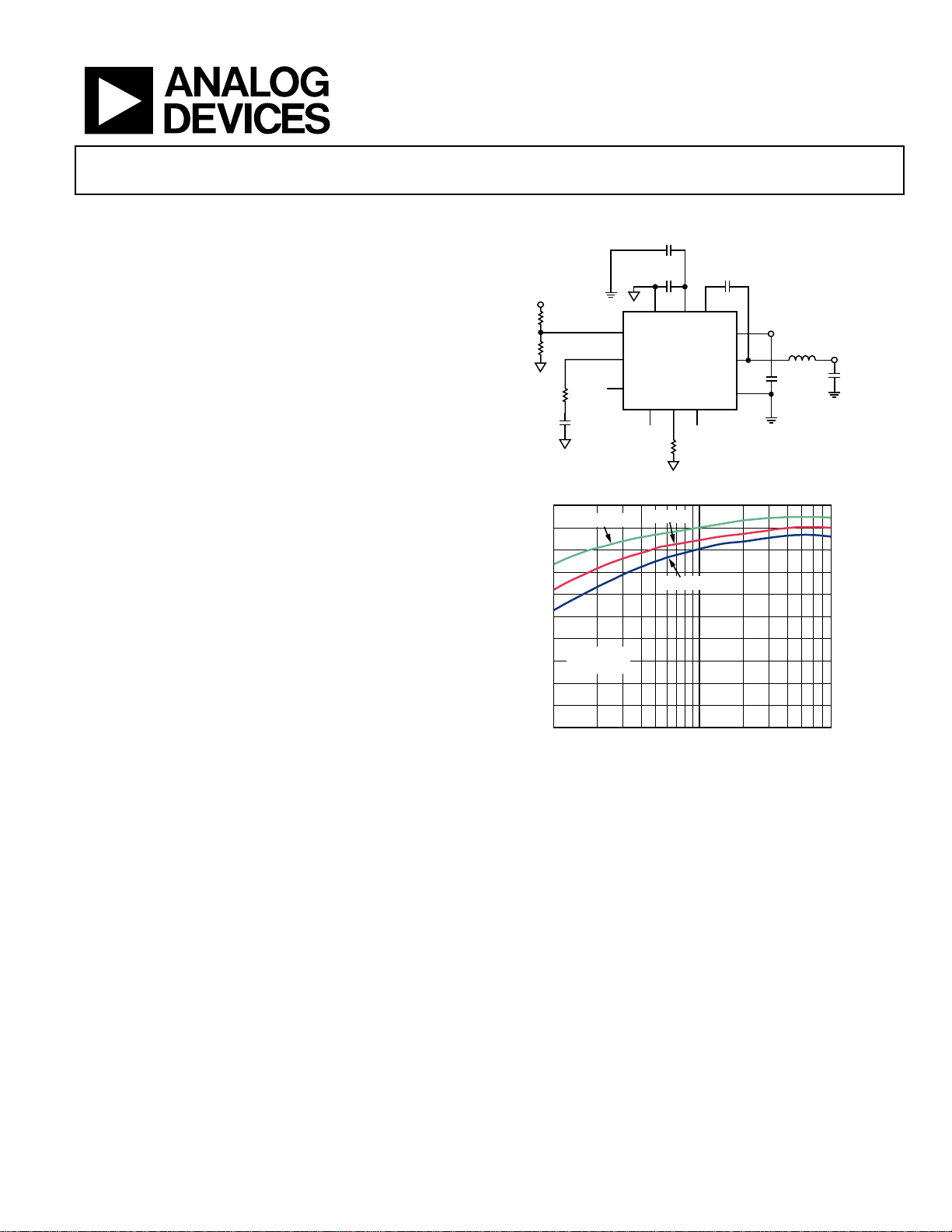
TYPICAL CIRCUIT CONFIGURATION
Figure 1.
GENERAL DESCRIPTION
The ADP2441 is a constant frequency, current mode control,
synchronous, step-down dc-to-dc regulator that is capable of
driving loads up to 1 A with excellent line and load regulation
characteristics. The ADP2441 operates with a wide input voltage
range of 4.5 V to 36 V, which makes it ideal for regulating power
from a wide variety of sources. In addition, the ADP2441 has
very low minimum on time (50 ns) and is, therefore, suitable for
applications requiring a very high step-down ratio.
The output voltage can be adjusted from 0.6 V to 0.9 V × V
High efficiency is obtained with integrated low resistance
N-channel MOSFETs for both high-side and low-side devices.
The switching frequency is adjustable from 300 kHz to 1 MHz with
an external resistor. The ADP2441 also has an accurate power-good
(PGOOD) open-drain output signal.
At light load conditions, the regulator operates in pulse skip
mode by skipping pulses and reducing switching losses to improve
energy efficiency. In addition, at medium to heavy load conditions,
the regulator operates in fixed frequency pulse-width modulation
(PWM) mode to reduce electromagnetic interference (EMI).
responsibility is assumed by Analog Devices for its use, nor for any infringements of patents or other
rights of third parties that may result from its use. Specifications subject to change without notice. No
license is granted by implication or otherwise under any patent or patent rights of Analog Devices.
.
IN
The ADP2441 uses hiccup mode to protect the IC from short
circuits or from overcurrent conditions on the output. The external
programmable soft start limits inrush current during startup for
a wide variety of load capacitances. Other key features include
tracking, input undervoltage lockout (UVLO), thermal shutdown
(TSD), and precision enable (EN), which can also be used as a
logic level shutdown input.
The ADP2441 is available in a 3 mm × 3 mm, 12-lead LFCSP
package and is rated for a junction temperature range of −40°C
to +125°C.
One Technology Way, P.O. Box 9106, Norwood, MA 02062-9106, U.S.A.
Tel: 781.329.4700
Figure 2. Efficiency vs. Load Current, VIN = 24 V
www.analog.com

ADP2441 Data Sheet
TABLE OF CONTENTS
Features .............................................................................................. 1
Applications ....................................................................................... 1
General Description ......................................................................... 1
Typical Circuit Configuration ......................................................... 1
Revision History ............................................................................... 2
Specifications ..................................................................................... 3
Absolute Maximum Ratings ............................................................ 5
Thermal Resistance ...................................................................... 5
ESD Caution .................................................................................. 5
Pin Configuration and Function Descriptions ............................. 6
Typical Performance Characteristics ............................................. 7
Internal Block Diagram ................................................................. 14
Theory of Operation ...................................................................... 15
Control Architecure ................................................................... 15
Adjustable Frequency ................................................................. 16
Power Good ................................................................................. 16
Soft Start ...................................................................................... 16
Tracking ....................................................................................... 16
Undervoltage Lockout (UVLO) ............................................... 17
Precision Enable/Shutdown ...................................................... 17
Current-Limit and Short-Circuit Protection .......................... 17
Thermal Shutdown ..................................................................... 17
Applications Information .............................................................. 18
Selecting the Output Voltage .................................................... 18
Setting the Switching Frequency .............................................. 18
Soft Start ...................................................................................... 19
External Components Selection ............................................... 19
Boost Capacitor .......................................................................... 21
VCC Capacitor............................................................................ 21
Loop Compensation .................................................................. 21
Large Signal Analysis of the Loop Compensation ................. 21
Design Example .............................................................................. 23
Configuration and Components Selection ............................. 23
System Configuration ................................................................ 24
Typical Application Circuits ......................................................... 25
Design Example .......................................................................... 25
Other Typical Circuit Configurations ..................................... 26
Power Dissipation and Thermal Considerations ....................... 29
Power Dissipation....................................................................... 29
Thermal Considerations ............................................................ 29
Evaluation Board Thermal Performance .................................... 30
Circuit Board Layout Recommendations ................................... 31
Outline Dimensions ....................................................................... 32
Ordering Guide .......................................................................... 32
REVISION HISTORY
6/12—Revision 0: Initial Version
Rev. 0 | Page 2 of 32

Data Sheet ADP2441
Hysteresis
200 mV
Feedback Regulation Voltage
VFB
TJ = −40°C to +85°C
0.594
0.6
0.606
V
Leakage Current
I
VEN = AGND
1 25
μA
Peak Current Limit
ICL 1.4
1.6
1.8
A
Frequency Set Accuracy
FREQ pin = 308 kΩ
270
300
330
kHz
Hysteresis
V
100 mV
SPECIFICATIONS
VIN = 4.5 V to 36 V, TJ = −40°C to +125°C, unless otherwise noted.
Table 1.
Parameter Symbol Test Conditions/Comments Min Typ Max Unit
POWER SUPPLY
Input Voltage Range VIN 4.5 36 V
Supply Current I
Shutdown Current I
UVLO
Threshold V
INTERNAL REGULATOR
Regulator Output Voltage VCC VIN = 5 V to 36 V 5 5.5 V
OUTPUT
Output Voltage Range V
Maximum Output Current I
TJ = −40°C to +125°C 0.591 0.6 0.609 V
Line Regulation 0.005 %/V
Load Regulation 0.05 %/A
ERROR AMPLIFIER
Feedback Bias Current I
Transconductance gm I
Open-Loop Voltage Gain1 A
MOSFETS
High-Side Switch On Resistance2 R
Low-Side Switch On Resistance2 R
Minimum On Time3 t
Minimum Off Time
4
CURRENT SENSE
Current Sense Amplifier Gain GCS 1.6 2 2.4 A/V
Hiccup Time fSW = 300 kHz to1 MHz 6 ms
Number Of Cumulative Current-Limit Cycles
to Go into Hiccup Mode
VEN = 1.5 V not switching 1.7 2.2 mA
VIN
VEN = AGND 10 15 µA
SHDN
VIN falling 3.8 4 4.2 V
UVLO
0.6 0.9 × VIN V
OUT
1 A
OUT
VFB = 0.6 V 50 200 nA
FB_BIAS
= ±20 µA 200 250 300 µA/V
COMP
65 dB
VOL
BST − SW = 5 V 170 270 mΩ
DS_H(ON)
VCC = 5 V 120 180 mΩ
DS_L(ON)
LKG
All switching frequencies 50 65 ns
ON_MIN
t
165 175 ns
OFF_MIN
8 Events
FREQUENCY
Switching Frequency Range fSW 300 1000 kHz
FREQ pin = 92.5 kΩ 900 1000 1100 kHz
SOFT START
Soft Start Current ISS VSS = 0 V 0.9 1 1.2 µA
PRECISION ENABLE
Input Threshold V
Leakage Current I
Thermal Shutdown
Rising TSD 150 °C
Hysteresis T
1.15 1.20 1.25 V
EN(RISING)
EN(HYST )
VIN = VEN 0.1 1 µA
IEN_LEAK
25 °C
SD(HYST )
Rev. 0 | Page 3 of 32

ADP2441 Data Sheet
PGOOD Low, FB Falling Threshold5
83
86
89
%
Parameter Symbol Test Conditions/Comments Min Typ Max Unit
POWER GOOD
PGOOD High, FB Rising Threshold5 89 92 95 %
PGOOD Low, FB Rising Threshold5 111 115 118 %
PGOOD High, FB Falling Threshold5 106 109 112 %
PGOOD
Delay t
High Leakage Current I
Pull-Down Resistor I
TRK
TRK Input Voltage Range 0 600 mV
TRK to FB Offset Voltage TRK = 0 mV to 500 mV 10 mV
1
Guaranteed by design.
2
Measured between VIN and SW pins—includes bond wires and pin resistance.
3
Based on bench characterization. Measured with VIN = 12 V, V
4
Based on bench characterization. Measured with VIN = 15 V, V
5
This threshold is expressed as a percentage of the nominal output voltage.
50 µs
PGOOD
V
PGOOD(SRC)
FB = 0 V 0.5 0.7 kΩ
PGOOD(SNK)
= 1.2 V, load = 1 A, fSW = 1 MHz, and the output in regulation. Measurement does not include dead time.
OUT
= 12 V, load = 1 A, fSW = 600 kHz, and the output in regulation. Measurement does not include dead time.
OUT
= VCC 1 10 µA
PGOOD
Rev. 0 | Page 4 of 32
Data Sheet ADP2441
EN to AGND
−0.3 V to +40 V
ABSOLUTE MAXIMUM RATINGS
Table 2.
Parameter Rating
VIN to PGND −0.3 V to +40 V
SW to PGND −0.3 V to +40 V
BST to PGND −0.3 V to +45 V
VCC to AGND −0.3 V to +6 V
BST to SW −0.3 V to +6 V
FREQ, PGOOD, SS/TRK, COMP, FB to AGND −0.3 V to +6 V
PGND to AGND ±0.3 V
Operating Junction Temperature Range −40°C to +125°C
Storage Temperature Range −65°C to +150°C
Lead Temperature (Soldering, 10 sec) 260°C
Stresses above those listed under Absolute Maximum Ratings
may cause permanent damage to the device. This is a stress
rating only; functional operation of the device at these or any
other conditions above those indicated in the operational
section of this specification is not implied. Exposure to absolute
maximum rating conditions for extended periods may affect
device reliability.
THERMAL RESISTANCE
θJA is specified for the worst-case conditions, that is, a device
soldered in a circuit board for surface-mount packages, and is
based on a 4-layer standard JEDEC board.
Table 3. Thermal Resistance
Package Type θJA θJC Unit
12-Lead LFCSP 40 2.4 °C/W
ESD CAUTION
Rev. 0 | Page 5 of 32

ADP2441 Data Sheet
FB
COMP
NOTES
1. THE EXPOSED PAD SHOULD BE CONNECTED
TO THE SYSTEMAGND P LANE AND PGND PLANE.
EN
VIN
SW
PGND
PGOOD
FREQ
SS/TRK
AGND
VCC
BST
10581-003
9
8
7
1
2
3
4
5
6
12
11
10
TOP
VIEW
ADP2441
PIN CONFIGURATION AND FUNCTION DESCRIPTIONS
Figure 3. Pin Configuration, Top View
Table 4. Pin Function Descriptions
Pin No. Mnemonic Description
1 FB Feedback Regulation Voltage is 0.6 V. Connect this pin to a resistor divider from the output of the dc-to-dc regulator.
2 COMP Error Amplifier Compensation. Connect a resistor and capacitor in series to ground.
3 EN Precision Enable. This features offers ±5% accuracy when using a 1.25 V reference voltage. Pull this pin high to
enable the regulator and low to disable the regulator.
4 PGOOD Active High Power-Good Output. This pin is pulled low when the output is out of regulation.
5 FREQ Switching Frequency. A resistor to AGND sets the switching frequency (see the Setting the Switching Frequency section).
6 SS/TRK Soft Start/Trac king Input. A capacitor to ground is required to program the soft start time, which gradually ramps
up the output. A resistive divider to an external reference is required on this pin to track an external voltage.
7 PGND Power Ground. Connect a decoupling ceramic capacitor as close as possible between the VIN pin and this pin.
Connect this pin directly to the exposed pad.
8 SW Switch. The midpoint for the drain of the low-side N-channel power MOSFET switch and the source for the high-side
N-channel power MOSFET switch.
9 VIN Power Supply Input. Connect this pin to the input power source, and connect a bypass ceramic capacitor directly
from this pin to PGND, as close as possible to the IC. The operation voltage is 4.5 V to 36 V.
10 BST Boost. Connect a 10 nF ceramic capacitor between the BST and SW pins as close to the IC as possible to form a
floating supply for the high-side N-Channel power MOSFET driver. This capacitor is needed to drive the gate of the
N-channel power MOSFET above the supply voltage.
11 VCC Output of the Internal Low Dropout Regulator. This pin supplies power for the internal controller and driver circuitry.
Connect a 1 µF ceramic capacitor between VCC and AGND and a 1 µF ceramic capacitor between VCC and PGND.
The VCC output is active when the EN pin voltage is more than 0.7 V.
12 AGND Analog Ground. This pin is the internal ground for the control functions. Connect this pin directly to the exposed pad.
EP Exposed Thermal Pad. The exposed pad should be connected to AGND and PGND.
Rev. 0 | Page 6 of 32
Data Sheet ADP2441
0
20
40
60
80
100
10
30
50
70
90
0.01 0.1
LOAD (A)
1
EFFICIENCY (%)
V
IN
= 5V
V
IN
= 24V
V
OUT
= 3.3V
f
SW
= 300kHz
COILCRAF T MSS1038
VIN= 12V
10581-004
0
20
40
60
80
100
10
30
50
70
90
0.01 0.1 1
EFFICIENCY (%)
LOAD (A)
VIN = 12V
10581-006
VIN= 24V
VIN= 36V
V
OUT
= 5V
f
SW
= 300kHz
COILCRAF T MSS1038
0
20
40
60
80
100
10
30
50
70
90
0.01 0.1 1
EFFICIENCY (%)
LOAD (A)
VIN = 24V
10581-008
VIN= 36V
V
OUT
= 12V
f
SW
= 300kHz
COILCRAF T MSS1038
0
20
40
60
80
100
10
30
50
70
90
0.01 0.1 1
EFFICIENCY (%)
LOAD (A)
V
IN
= 5V
VIN= 12V
VIN= 24V
V
OUT
= 3.3V
f
SW
= 700kHz
COILCRAF T MSS1038
10581-005
0
20
40
60
80
100
10
30
50
70
90
0.01 0.1 1
EFFICIENCY (%)
LOAD (A)
VIN = 12V
10581-007
VIN= 36V
V
OUT
= 5V
f
SW
= 700kHz
COILCRAF T MSS1038
VIN= 24V
0
20
40
60
80
100
10
30
50
70
90
0.01 0.1 1
EFFICIENCY (%)
LOAD (A)
10581-009
V
OUT
= 12V
f
SW
= 600kHz
COILCRAF T MSS1038
VIN = 24V
VIN= 36V
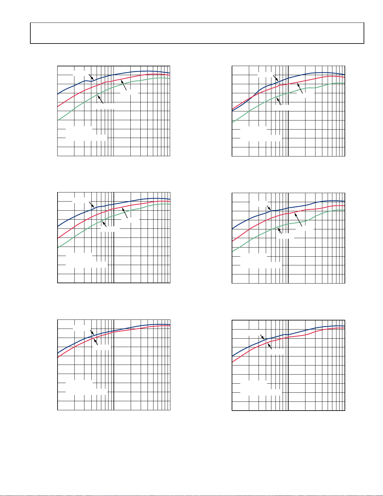
TYPICAL PERFORMANCE CHARACTERISTICS
Figure 4. Efficiency vs. Load Current,
V
= 3.3 V, fSW = 300 kHz
OUT
Figure 5. Efficiency vs. Load Current,
V
= 5 V, fSW = 300 kHz
OUT
Figure 7. Efficiency vs. Load Current,
V
= 3.3 V, fSW = 700 kHz
OUT
Figure 8. Efficiency vs. Load Current,
V
= 5 V, fSW = 700 kHz
OUT
Figure 6. Efficiency vs. Load Current,
V
= 12 V, fSW = 300 kHz
OUT
Figure 9. Efficiency vs. Load Current,
V
= 12 V, fSW = 600 kHz
OUT
Rev. 0 | Page 7 of 32
ADP2441 Data Sheet
–0.5
–0.4
–0.3
–0.2
–0.1
0
0.1
0.2
0.3
0.4
0.5
0 0.2 0.4 0.6 0.8 1.0
V
OUT
ERROR (%)
LOAD (A)
V
IN
= 12V
V
IN
= 24V
V
IN
= 36V
V
OUT
= 5V
f
SW
= 700kHz
10581-010
1.0
0 0.2 0.4 0.6 0.8 1.0
V
OUT
ERROR (%)
LOAD (A)
T
A
= –40°C
T
A
= +25°C
T
A
= +125°C
10581-011
VIN= 24V
V
OUT
= 5V
f
SW
= 700kHz
–0.5
–0.4
–0.3
–0.2
–0.1
0
0.1
0.2
0.3
0.4
0.5
7 12 17 22 27 32 37
V
OUT
ERROR (%)
VIN (V)
LOAD = 500mA
LOAD = 1A
10581-012
VIN= 24V
V
OUT
= 5V
f
SW
= 700kHz
0
50
100
150
200
250
300
350
400
5 10 15 20 25 30 35 40
P
SKIP
THRESHOL D LOAD CURRENT (mA)
VIN (V)
f
SW
= 300kHz
f
SW
= 700kHz
V
OUT
= 3.3V
10581-013
0
50
100
150
200
250
300
10 15 20 25 30 35 40
P
SKIP
THRESHOL D LOAD CURRENT (mA)
VIN (V)
f
SW
=
700kHz
10581-014
V
OUT
= 5V
f
SW
=
300kHz
0
50
100
150
200
250
300
15 20 25 30 35 40
P
SKIP
THRESHOL D LOAD CURRENT (mA)
VIN (V)
f
SW
=
300kHz
f
SW
=
600kHz
10581-015
V
OUT
= 12V
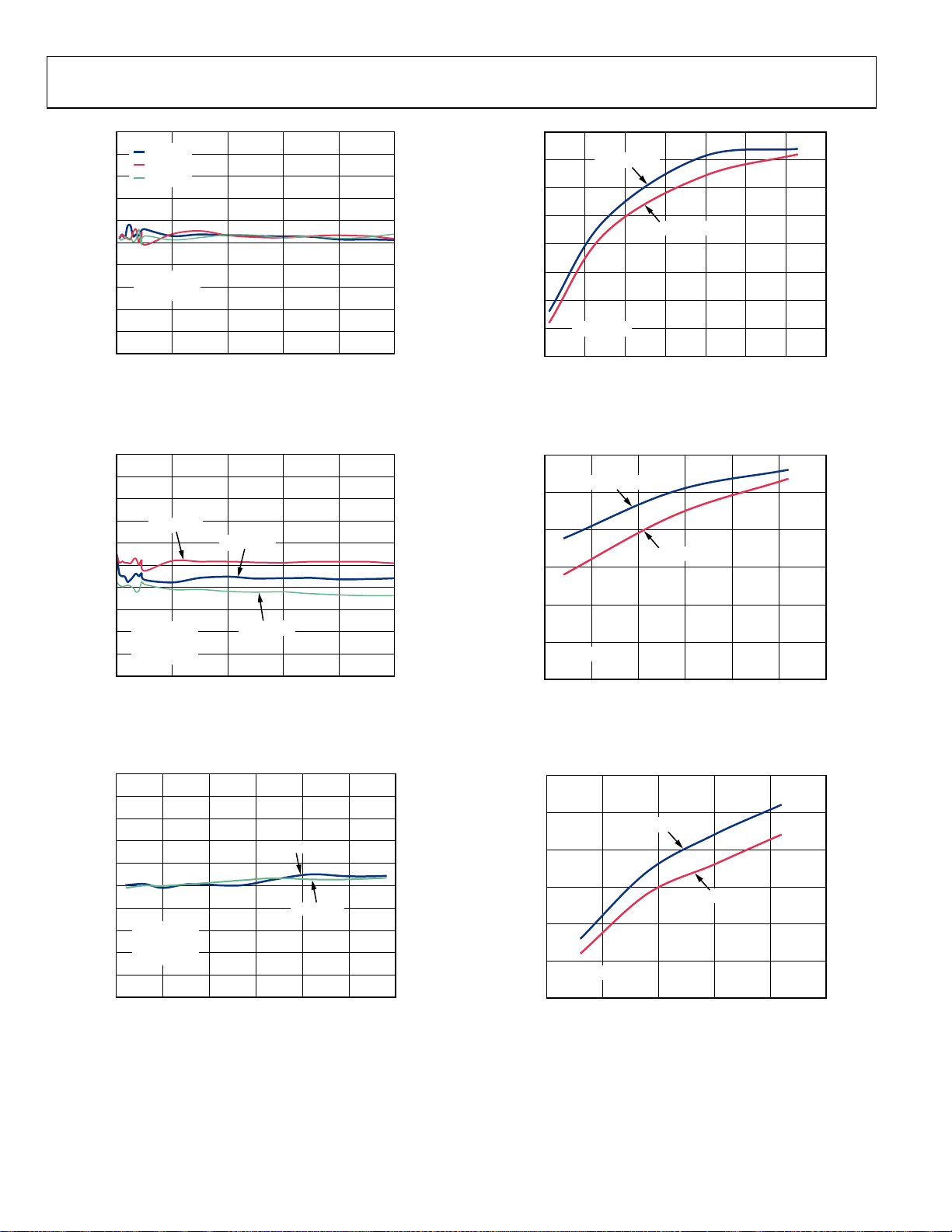
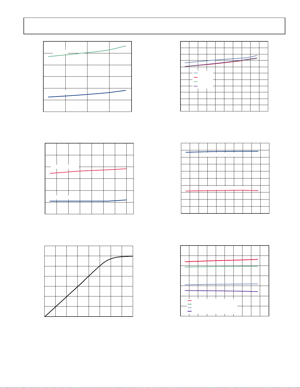
Figure 10. Load Regulation for Different Supplies
0.8
0.6
0.4
0.2
0
–0.2
–0.4
–0.6
–0.8
–1.0
Figure 13. Pulse Skip Threshold, V
OUT
= 3.3 V
Figure 11. Load Regulation for Different Temperatures
Figure 12. Line Regulation, V
OUT
= 5 V for Different Loads
Rev. 0 | Page 8 of 32
Figure 14. Pulse Skip Threshold, V
Figure 15. Pulse Skip Threshold, V
OUT
OUT
= 5 V
= 12 V
Data Sheet ADP2441
0
2
4
8
6
10
12
–50 0 50 100 150
SHUTDOWN CURE NT (µA)
TEMPERATURE (°C)
V
IN
= 36V
V
IN
= 4.5V
10581-017
UVLO THRE S HOLD (V)
TEMPERATURE (°C)
10581-018
3.9
4.0
4.1
4.2
4.3
4.4
4.5
–50 –25 0 25 50 75 100 125
UVLO, RISING V
IN
UVLO, FALLING V
IN
0
0.1
0.2
0.3
0.4
0.5
0.6
0.7
0 0.1 0.2 0.3 0.4 0.5 0.6 0.7 0.8
FB (V)
TRACK (V)
10581-118
0.05
0.25
0.45
0.65
0.85
1.05
1.25
1.45
1.65
1.85
2.05
2.25
–50 –30 –10 10 30 50 70 90 110 130 150
SUPPLY CURRENT ( mA)
TEMPERATURE (°C)
V
IN
= 36V
V
IN
= 24V
V
IN
= 12V
V
IN
= 4.5V
10581-016
1.04
1.06
1.08
1.10
1.12
1.14
1.16
1.18
1.20
1.22
1.24
–50 –30 –10 10 30 50 70 90 110 130 150
ENABLE VOLTAGE (V)
TEMPERATURE (°C)
ENABLE RISING THRESHOLD
ENABLE FALLING THRESHOLD
10581-019
60
70
80
90
100
110
120
130
–50 –30 –10 10 30 50 70 90 110 130 150
PGOOD THRESHOLD (%)
TEMPERATURE (°C)
P
GOOD
RISE, F B INCREASING
P
GOOD
FALL, FB INCREASING
P
GOOD
RISE, F B DE CRE AS ING
P
GOOD
FALL, FB DECREASING
10581-021
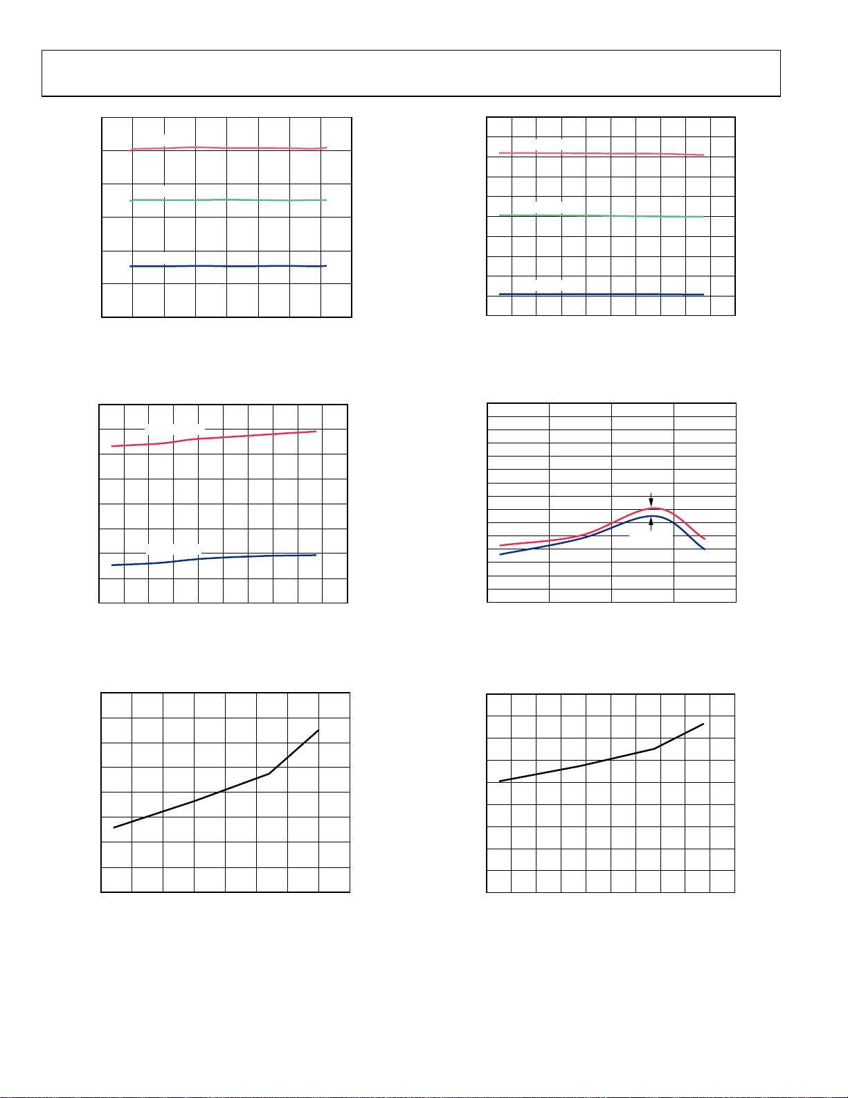
Figure 16. Shutdown Current vs. Temperature
Figure 17. UVLO Threshold vs. Temperature
Figure 19. Supply Current vs. Temperature
Figure 20. Enable Threshold vs. Temperature
Figure 18. Tracking Range
Figure 21. PGOOD Threshold vs. Temperature
Rev. 0 | Page 9 of 32
ADP2441 Data Sheet
0
200
400
600
800
1000
1200
0 5 10 15 20 25 30 35 40
SWITCHING FREQUE NCY (kHz)
VIN (V)
f
SW
= 300kHz
f
SW
= 1MHz
f
SW
= 700kHz
10581-022
0
25
50
75
100
125
150
175
200
–50 –30 –10 10 30 50 70 90 110 130 150
ON TIMEAND OFF TIME (ns)
TEMPERATURE (°C)
MINIMUM ON
MINIMUM OFF
10581-024
100
120
140
160
180
200
220
240
260
–50 –25 0 25 50 75 100 125 150
HIGH-SI DE R
DS(ON)
(mΩ)
TEMPERATURE (°C)
10581-027
200
300
400
500
600
700
800
900
1000
1100
1200
–50 –30 –10 10 30 50 70 90 110 130 150
FREQUENCY (kHz)
TEMPERATURE (°C)
f
SW
= 300kHz
f
SW
= 1MHz
f
SW
= 700kHz
10581-023
1.50
1.52
1.54
1.56
1.58
1.60
1.62
1.64
1.66
1.68
1.70
1.72
1.74
1.76
1.78
1.80
–50 0 50 100 150
CURRENT (A)
TEMPERATURE (°C)
V
IN
= 36V
VIN = 4.5V
10581-126
0
20
40
60
80
100
120
140
160
180
–50 –30 –10 10 30 50 70 90 110 130 150
LOW-SIDE R
DS(ON)
(mΩ)
TEMPERATURE (°C)
10581-026
Figure 22. Switching Frequency vs. Supply
Figure 23. Minimum On Time and Minimum Off Time vs. Temperature
Figure 25. Switching Frequency vs. Temperature
Figure 26. Current Limit vs. Temperature
Figure 24. High-Side R
vs. Temperature
DS(ON)
Figure 27. Low-Side R
vs. Temperature
DS(ON)
Rev. 0 | Page 10 of 32
 Loading...