Regulator with Low-Side Driver
ADP2381
ADP2381
10209-001
1
PVIN
PVIN
UVLO
PGOOD
RT
SYNC
EN/SS
COMP
BST
SW
SW
LD
VREG
PGND
GND
FB
2
3
4
5
6
7
8
16
15
14
13
12
11
10
9
R
OSC
R
TOP
R
BOT
C
SS
C
IN
C
OUT
V
OUT
C
BST
C
VREG
L
V
IN
C
C_EA
C
CP_EA
R
C_EA
FET
100
50
55
60
65
70
75
80
85
90
95
0 1 2 3 4 5 6
EFFICIENCY (%)
OUTPUT CURRE NT (A)
10209-002
V
OUT
= 3.3V
V
OUT
= 5V
V
OUT
= 1.2V
Rev. 0
Information furnished by Analog Devices is believed to be accurate and reliable. However, no
Trademarks and registered trademarks are the property of their respective owners.
Fax: 781.461.3113 ©2012 Analog Devices, Inc. All rights reserved.
Data Sheet
FEATURES
Input voltage: 4.5 V to 20 V
Integrated 44 mΩ high-side MOSFET
0.6 V ± 1% reference voltage over temperature
Continuous output current: 6 A
Programmable switching frequency: 250 kHz to 1.4 MHz
Synchronizes to external clock: 250 kHz to 1.4 MHz
180° out-of-phase synchronization
Programmable UVLO
Power-good output
External compensation
Internal soft start with external adjustable option
Startup into a precharged output
Supported by ADIsimPower design tool
APPLICATIONS
Communication infrastructure
Networking and servers
Industrial and instrumentation
Healthcare and medical
Intermediate power rail conversion
DC-to-dc point of load application
20 V, 6 A Synchronous Step-Down
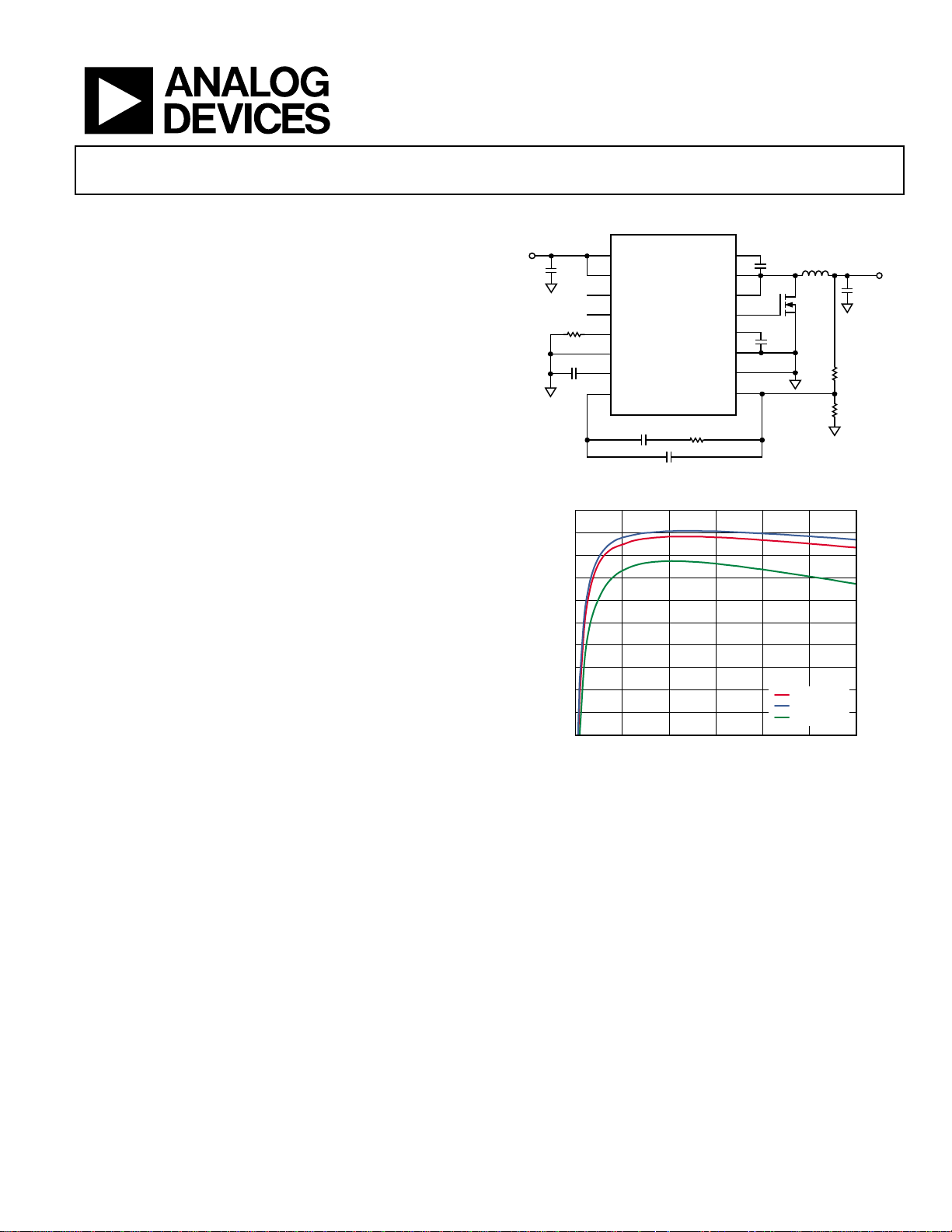
TYPICAL APPLICATIONS CIRCUIT
Figure 1.
GENERAL DESCRIPTION
The ADP2381 is a current mode control, synchronous, stepdown, dc-to-dc regulator. It integrates a 44 mΩ power MOSFET
and a low-side driver to provide a high efficiency solution. The
ADP2381 runs from an input voltage of 4.5 V to 20 V and can
deliver 6 A of output current. The output voltage can be
adjusted to 0.6 V to 90% of the input voltage. The switching
frequency of the ADP2381 can be programmed from
250 kHz to 1.4 MHz or fixed at 290 kHz or 550 kHz. The
synchronization function allows the switching frequency to be
synchronized to an external clock to minimize system noise.
responsibility is assumed by Analog Devices for its use, nor for any infringements of patents or other
rights of third parties that may result from its use. Specifications subject to change without notice. No
license is granted by implication or otherwise under any patent or patent rights of Analog Devices.
External compensation and an adjustable soft start provide
design flexibility. The power-good output provides simple and
reliable power sequencing. Additional features include
programmable undervoltage lockout (UVLO), overvoltage
protection (OVP), overcurrent protection (OCP), and thermal
shutdown (TSD).
The ADP2381 operates over the −40°C to +125°C junction
temperature range and is available in a 16-lead TSSOP_EP
package.
One Technology Way, P.O. Box 9106, Norwood, MA 02062-9106, U.S.A.
Tel: 781.329.4700
Figure 2. ADP2381 Efficiency vs. Output Current, V
= 12 V, fSW = 250 kHz
IN
www.analog.com

ADP2381 Data Sheet
TABLE OF CONTENTS
Features .............................................................................................. 1
Applications ....................................................................................... 1
Typical Applications Circuit ............................................................ 1
General Description ......................................................................... 1
Revision History ............................................................................... 2
Specifications ..................................................................................... 3
Absolute Maximum Ratings ............................................................ 5
Thermal Information ................................................................... 5
ESD Caution .................................................................................. 5
Pin Configuration and Function Description .............................. 6
Typical Performance Characteristics ............................................. 7
Functional Block Diagram ............................................................ 12
Theory of Operation ...................................................................... 13
Control Scheme .......................................................................... 13
Internal Regulator (VREG) ....................................................... 13
Bootstrap Circuitry .................................................................... 13
Low-Side Driver .......................................................................... 13
Oscillator ..................................................................................... 13
Synchronization .......................................................................... 13
Enable and Soft Start .................................................................. 13
Power Good ................................................................................. 14
Peak Current Limit and Short-Circuit Protection ................. 14
Overvoltage Protection (OVP) ................................................. 14
Undervoltage Lockout (UVLO) ................................................ 14
Thermal Shutdown ..................................................................... 14
Applications Information .............................................................. 15
Input Capacitor Selection .......................................................... 15
Output Voltage Setting .............................................................. 15
Voltage Conversion Limitations ............................................... 15
Inductor Selection ...................................................................... 15
Output Capacitor Selection....................................................... 17
Low-Side Power Device Selection ............................................ 17
Programming Input Voltage UVLO ........................................ 18
Compensation Design ............................................................... 18
ADIsimPower Design Tool ....................................................... 19
Design Example .............................................................................. 20
Output Voltage Setting .............................................................. 20
Frequency Setting ....................................................................... 20
Inductor Selection ...................................................................... 20
Output Capacitor Selection....................................................... 20
Low-Side MOSFET Selection ................................................... 21
Compensation Components ..................................................... 21
Soft Start Time Program ........................................................... 21
Input Capacitor Selection .......................................................... 21
Schematic for Design Example ................................................. 21
External Components Recommendation .................................... 23
Circuit Board Layout Recommendations ................................... 25
Typical Application Circuits ......................................................... 27
Outline Dimensions ....................................................................... 28
Ordering Guide .......................................................................... 28
REVISION HISTORY
3/12—Revision 0: Initial Version
Rev. 0 | Page 2 of 28

Data Sheet ADP2381
PVIN
SHDN
EA Source Current
I
SOURCE
40
60
80
µA
SINK
VREG
PVIN
VREG
PVIN
VREG
BST
MIN_ON
SW Minimum Off Time
t
MIN_OFF
200
300
ns
BOOT
OSCILLATOR (RT PIN)
OSC
SS_UP
SPECIFICATIONS
VIN = 12 V, TJ = −40°C to +125°C for min/max specifications, and TA = 25°C for typical specifications, unless otherwise noted.
Table 1.
Parameter Symbol Test Conditions/Comments Min Typ Max Unit
PVIN
PVIN Voltage Range V
Quiescent Current IQ No switching 2 2.8 3.5 mA
Shutdown Current I
PVIN Undervoltage Lockout Threshold PVIN rising 4.3 4.5 V
FB
FB Regulation Voltage VFB 0°C < TJ < 85°C 0.594 0.6 0.606 V
FB Bias Current IFB 0.01 0.1 µA
ERROR AMPLIFIER (EA)
Transconductance gm 360 500 620 µS
4.5 20 V
EN/SS = GND 80 130 170 µA
PVIN falling 3.7 3.9 V
−40°C < TJ < +125°C 0.591 0.6 0.609 V
EA Sink Current I
40 60 80 µA
INTERNAL REGULATO R (VREG)
VREG Voltage V
Dropout Voltage V
V
= 12 V, I
= 12 V, I
= 50 mA 7.6 8 8.4 V
= 50 mA 350 mV
Regulator Current Limit 65 100 135 mA
SW
High-Side On Resistance1 V
− VSW = 5 V 44 70 mΩ
High-Side Peak Current Limit 7.7 9.6 11.5 A
Negative Current-Limit Threshold Voltage2 20 mV
SW Minimum On Time t
120 170 ns
LOW-SIDE DRIVER (LD)
Rising Time2 tR CDL = 2.2 nF; see Figure 17 20 ns
Falling Time2 tF CDL = 2.2 nF; see Figure 20 10 ns
Sourcing Resistor 4 6 Ω
Sinking Resistor 2 3.5 Ω
BST
Bootstrap Voltage V
Switching Frequency
4.5 5 5.7 V
fSW RT pin connected to GND 210 290 360 kHz
RT pin open 400 550 690 kHz
R
= 100 kΩ 425 500 570 kHz
Switching Frequency Range fSW 250 1400 kHz
SYNC
Synchronization Range 250 1400 kHz
SYNC Minimum Pulse Width 100 ns
SYNC Minimum Off Time 100 ns
SYNC Input High Voltage 1.3 V
SYNC Input Low Voltage 0.4 V
EN/SS
Enable Threshold 0.5 V
Internal Soft Start 1500 Clock cycles
SS Pin Pull-Up Current I
2.6 3.3 4 µA
Rev. 0 | Page 3 of 28

ADP2381 Data Sheet
PGOOD from high to low
16 Clock cycles
PGOOD
PGOOD
THERMAL
Parameter Symbol Test Conditions/Comments Min Typ Max Unit
POWER GOOD (PGOOD)
PGOOD Range FB rising threshold 95 %
FB falling threshold 90 %
PGOOD Deglitch Time PGOOD from low to high 1024 Clock cycles
PGOOD Leakage Current V
PGOOD Output Low Voltage I
= 5 V 0.01 0.1 µA
= 1 mA 125 200 mV
UVLO
Rising Threshold 1.2 1.28 V
Falling Threshold 1.02 1.1 V
Thermal Shutdown Threshold 150
Thermal Shutdown Hysteresis 25
1
Pin-to-pin measurement.
2
Guaranteed by design.
°C
°C
Rev. 0 | Page 4 of 28
Data Sheet ADP2381
SW
−1 V to +22 V
Storage Temperature Range
−65°C to +150°C
Package Type
θ
JA
Unit
ABSOLUTE MAXIMUM RATINGS
Table 2.
Parameter Rating
PVIN, PGOOD −0.3 V to +22 V
BST VSW + 6 V
UVLO, FB, EN/SS, COMP, SYNC, RT
VREG, LD −0.3 V to +12 V
PGND to GND −0.3 V to +0.3 V
Operating Junction Temperature Range −40°C to +125°C
Soldering Conditions JEDEC J-STD-020
Stresses above those listed under Absolute Maximum Ratings
may cause permanent damage to the device. This is a stress
rating only; functional operation of the device at these or any
other conditions above those indicated in the operational
section of this specification is not implied. Exposure to absolute
maximum rating conditions for extended periods may affect
device reliability.
−0.3 V to +6 V
Absolute maximum ratings apply individually only, not in
combination. Unless otherwise specified, all other voltages are
referenced to GND.
THERMAL INFORMATION
Table 3. Thermal Resistance
16-lead TSSOP_EP 39.48 °C/W
θJA is specified for the worst-case conditions, that is, a device
soldered in circuit board (4-layer, JEDEC standard board) for
surface-mount packages.
ESD CAUTION
Rev. 0 | Page 5 of 28

ADP2381 Data Sheet
OUT
12
VREG
Internal 8 V Regulator Output. Place a 1 µF ceramic capacitor between this pin and GND.
TOP VIEW
(Not to S cale)
1
2
3
4
5
6
7
8
ADP2381
16
15
14
13
12
11
10
9
PVIN
UVLO
PGOOD
EN/SS
SYNC
RT
PVIN
SW
SW
LD
GND
COMP FB
PGND
VREG
BST
10209-003
NOTES
1. THE EXPOSED PAD SHOULD BE SOLDERED
TO AN EXT E RNAL GROUND PLANE UNDE RNE ATH
THE IC FOR THERMAL DISSIPATION.
PIN CONFIGURATION AND FUNCTION DESCRIPTION
Figure 3. Pin Configuration (Top View)
Table 4. Pin Function Descriptions
Pin No. Mnemonic Description
1, 2 PVIN Power Input. Connect to the input power source and connect a bypass capacitor between this pin and
PGND.
3 UVLO Undervoltage Lockout Pin. An external resistor divider can be used to set the turn-on threshold.
4 PGOOD Power-Good Output (Open Drain). A pull-up resistor of 10 kΩ to 100 kΩ is recommended.
5 RT Frequency Setting. Connect a resistor between RT and GND to program the switching frequency
between 250 kHz and 1.4 MHz. If the RT pin is connected to GND, the switching frequency is set to 290
kHz. If the RT pin is open, the switching frequency is set to 550 kHz.
6 SYNC Synchronization Input. Connect this pin to an external clock to synchronize the switching frequency
between 250 kHz and 1.4 MHz (see the Oscillator section and the Synchronization section for details).
7 EN/SS Enable Pin (EN). When this pin voltage falls below 0.5 V, the regulator is disabled.
Soft Start (SS). This pin can also be used to set the soft start time.
Connect a capacitor from SS to GND to program the slow soft start time. If this pin is open, the regulator
is enabled and uses the internal soft start.
8 COMP Error Amplifier Output. Connect an RC network from COMP to FB.
9 FB Feedback Voltage Sense Input. Connect to a resistor divider from V
.
10 GND Analog Ground. Connect to the ground plane.
11 PGND Power Ground. Connect to the source of the synchronous N-channel MOSFET.
13 LD Low-Side Gate Driver Output. Connect this pin to the gate of the synchronous N-MO SFET.
14, 15 SW Switch Node Output. Connect this pin to the output inductor.
16 BST Supply Rail for the High-Side Gate Drive. Place a 0.1 µF ceramic capacitor between SW and BST.
17 EPAD The exposed pad should be soldered to an external ground plane underneath the IC for thermal
dissipation.
Rev. 0 | Page 6 of 28
Data Sheet ADP2381
100
50
55
60
65
70
75
80
85
90
95
0 1 2 3 4 5 6
EFFICIENCY (%)
OUTPUT CURRE NT (A)
10209-004
V
OUT
= 1.2V
V
OUT
= 1.8V
V
OUT
= 2.5V
V
OUT
= 3.3V
V
OUT
= 5V
INDUCTOR: FDVE1040-2R2M
MOSFET: FDS6298
100
50
55
60
65
70
75
80
85
90
95
0 1 2 3 4 5 6
EFFICIENCY (%)
OUTPUT CURRE NT (A)
10209-005
V
OUT
= 1.8V
V
OUT
= 2.5V
V
OUT
= 3.3V
V
OUT
= 5V
INDUCTOR: FDVE1040-3R3M
MOSFET: FDS6298
10209-006
90
100
110
120
130
140
150
160
4 6 8 10 12 14 16 18 20
SHUTDOWN CURRENT (μA)
VIN (V)
TJ = –40°C
TJ = +25°C
TJ = +125°C
100
50
55
60
65
70
75
80
85
90
95
0 1 2 3 4 5 6
EFFICIENCY (%)
OUTPUT CURRE NT (A)
10209-007
V
OUT
= 1.2V
V
OUT
= 1.8V
V
OUT
= 2.5V
V
OUT
= 3.3V
V
OUT
= 5V
INDUCTOR: FDVE1040-4R7M
MOSFET: FDS6298
100
50
55
60
65
70
75
80
85
90
95
0 1 2 3 4 5 6
EFFICIENCY (%)
OUTPUT CURRE NT (A)
10209-008
V
OUT
= 1.0V
V
OUT
= 1.2V
V
OUT
= 1.5V
V
OUT
= 1.8V
V
OUT
= 2.5V
V
OUT
= 3.3V
INDUCTOR: 744 333 0100
MOSFET: FDS6298
1.80
2.00
2.20
2.40
2.60
2.80
3.00
3.20
4 6 8 10 12 14 16 18 20
QUIESCENT CURRENT (mA)
VIN (V)
10209-009
TJ = –40°C
T
J
= +25°C
TJ = +125°C
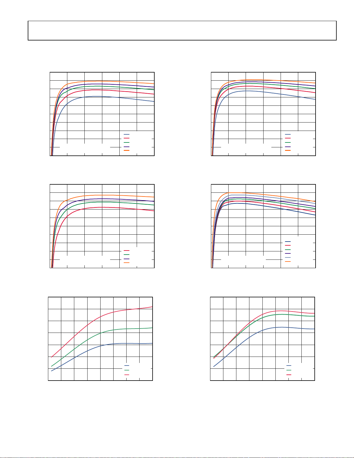
TYPICAL PERFORMANCE CHARACTERISTICS
Operating conditions: TA = 25oC, VIN = 12 V, V
= 3.3 V, L = 2.2 µH, C
OUT
= 2 × 100 µF, fSW = 500 kHz, unless otherwise noted.
OUT
Figure 4. Efficiency at VIN = 12 V, fSW = 500 kHz
Figure 5. Efficiency at VIN = 18 V, fSW = 500 kHz
Figure 7. Efficiency at VIN = 12 V, fSW = 250 kHz
Figure 8. Efficiency at VIN = 5 V, fSW = 500 kHz
Figure 6. Shutdown Current vs. VIN
Figure 9. Quiescent Current vs. VIN
Rev. 0 | Page 7 of 28
ADP2381 Data Sheet
4.5
PVIN UVLO THRESHOLD (V)
10209-011
3.30
2.90
–40 120
SS PULL- UP CURRE NT (µA)
TEMPERATURE (°C)
2.95
3.00
3.05
3.10
3.15
3.20
3.25
–20 0 20 40 60 80 100
530
520
510
470
480
490
500
–40 120
FREQUENCY ( kHz )
TEMPERATURE (°C)
10209-012
–20 0 20 40 60 80 100
R
OSC
= 100kΩ
10209-013
1.00
1.30
–40 –20 0 20 40 60 80 100 120
UVLO PI N THRESHOLD (V )
TEMPERATURE (°C)
1.05
1.10
1.15
1.20
1.25
RISING
FALLING
606
604
602
594
596
598
600
–40 120
FEEDBACK VOLTAGE (mV)
TEMPERATURE (°C)
10209-014
–20 0 20 40 60 80 100
10209-015
8.4
7.6
–40 120
VREG VOLTAGE (V)
TEMPERATURE (°C)
7.7
7.8
7.9
8.0
8.1
8.2
8.3
–20 0 20 40 60 80 100
4.4
4.3
4.2
4.1
4.0
3.9
3.8
3.7
3.6
–40 –20 0 20 40 60 80 100 120
RISING
FALLING
TEMPERATURE (°C)
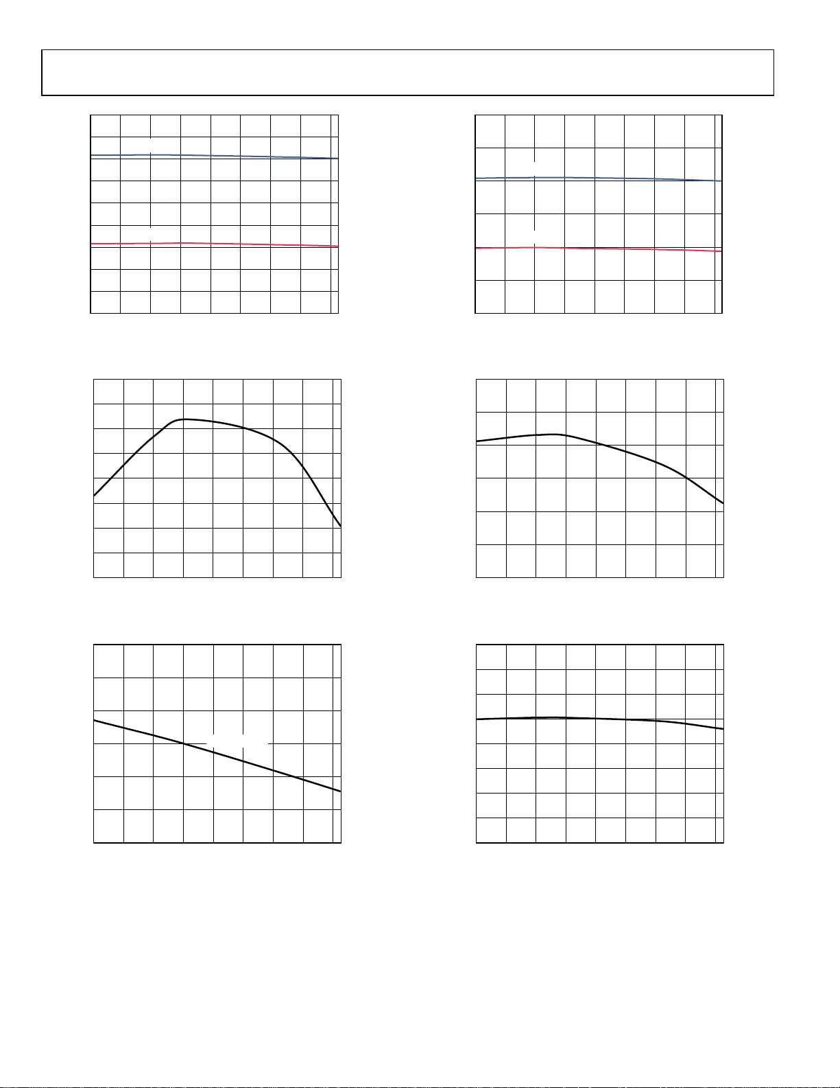
Figure 10. PVIN UVLO Threshold vs. Temperature
10209-010
Figure 13. UVLO Pin Threshold vs. Temperature
Figure 11. SS Pin Pull-Up Current vs. Temperature
Figure 12. Frequency vs. Temperature
Figure 14. FB Voltage vs. Temperature
Figure 15. VREG Voltage vs. Temperature
Rev. 0 | Page 8 of 28
Data Sheet ADP2381
70
60
20
30
40
50
–40 120
MOSFET R
DSON
(mΩ)
TEMPERATURE (°C)
10209-016
–20 0 20 40 60 80 100
10209-017
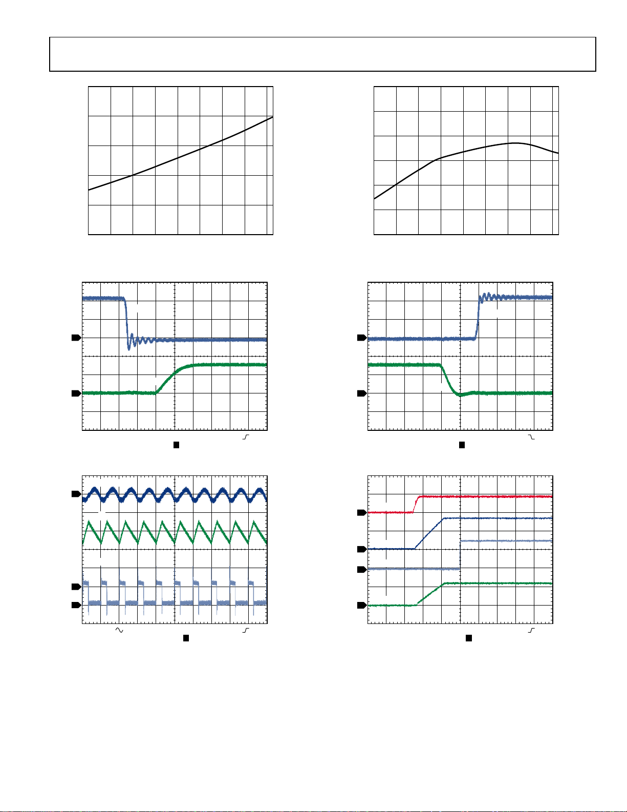
CH2 5.00VCH1 5.00V M20.0ns A CH2 3.70V
1
2
T 46.60%
SW
LD
10209-018
CH2 10V
CH4 2A Ω
CH1 10mV
B
W
M2.00µs A CH2 6.00V
4
2
1
T 50.00%
V
OUT
(AC)
I
L
SW
11.0
10.5
10.0
8.0
8.5
9.0
9.5
–40 120
PEAK CURRENT LIMIT THRE S HOLD (A)
TEMPERATURE (°C)
10209-019
–20 0 20 40 60 80 100
10209-020
CH2 5.00VCH1 5.00V M20.0ns A CH2 3.70V
1
2
T 43.80%
SW
LD
10209-021
CH2 5.00V
CH4 5.00A Ω
CH1 2.00V
CH3 5.00V
M2.00ms A CH2 5.80V
1
3
2
4
T 50.00%
EN/SS
PGOOD
V
OUT
I
OUT
B
W
Figure 16. MOSFET R
vs. Temperature
DSON
Figure 17. Low-Side Driver Rising Edge Waveform, CDL = 2.2 nF
Figure 19. Current-Limit Threshold vs. Temperature
Figure 20. Low-Side Driver Falling Edge Waveform, CDL = 2.2 nF
Figure 18. Working Mode Waveform
Figure 21. Soft Start with Full Load
Rev. 0 | Page 9 of 28
 Loading...