High Voltage, 1.2 MHz/600 kHz, 800 mA,
Low Quiescent Current Buck Regulator
ADP2370/ADP2371
Trademarks and registered trademarks are the property of their respective owners.
Fax: 781.461.3113 ©2012 Analog Devices, Inc. All rights reserved.
ADP2370/
ADP2371
FSEL
EN
POWER GOOD
V
OUT
= 3.3V
V
IN
= 6V
C
IN
10µF
C
OUT
10µF
AGND
(EXPOSED PAD)
VIN
SYNC
ON
OFF
1.2MHz
600kHz
SW
PG
PGND
FB
1
2
3
4
8
7
6
5
09531-001
Data Sheet
FEATURES
Input voltage range: 3.2 V to 15 V, output current: 800 mA
Quiescent current < 14 µA in power saving mode (PSM)
>90% efficiency
Force PWM pin (SYNC), 600 kHz/1.2 MHz frequency pin
(FSEL)
Fixed outputs: 0.8 V, 1.2 V, 1.5 V, 1.8 V, 2.5 V, 3.0 V, 3.3 V, 5 V,
and adjustable option
100% duty cycle capability
Initial accuracy: ±1%
Low shutdown current: <1.2 µA
Quick output discharge (QOD) option
Synchronizable to an external clock
8-lead, 0.75 mm × 3 mm × 3 mm LFCSP (QFN) package
Supported by ADIsimPower design tool
APPLICATIONS
Portable and battery-powered equipment
Automatic meter readers (WSN)
Point of sales and transaction processing instruments
Medical instruments
Medium format display tablets and pads
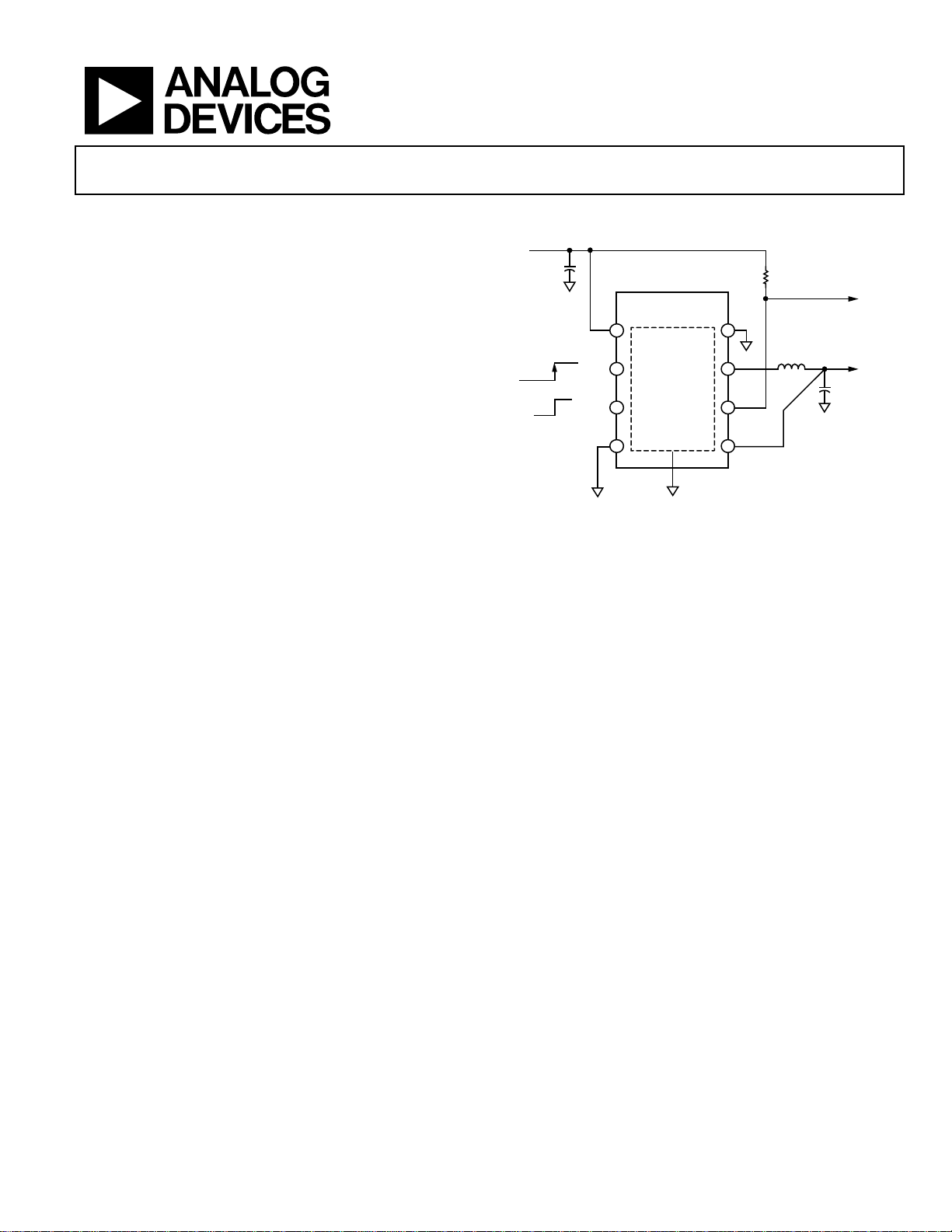
TYPICAL APPLICATION CIRCUIT
Figure 1.
GENERAL DESCRIPTION
The ADP2370/ADP2371 are high efficiency, low quiescent current,
800 mA buck (step-down) dc-to-dc converters in small 8-lead,
3 mm × 3 mm LFCSP (QFN) packages. The total solution requires
only three tiny external components.
The buck regulator uses a proprietary high speed current mode,
constant frequency PWM control scheme for excellent stability
and transient response. The need for an external rectifier is eliminated by using a high efficiency synchronous rectifier architecture.
To ensure the longest battery life in portable applications, the
ADP2370/ADP2371 employ a power saving variable frequency
mode that reduces the switching frequency under light load
conditions. The ADP2370/ADP2371 operate from input voltages
of 3.2 V to 15 V allowing the use of multiple alkaline/NiMH,
lithium cells, or other standard power sources.
The ADP2370/ADP2371 offer multiple options for setting the
operational frequency. The ADP2370/ADP2371 can be synchronized to a 600 kHz to 1.2 MHz external clock or it can be forced
to operate at 600 kHz or 1.2 MHz via the FSEL pin. The ADP2370/
ADP2371 can be forced to operate in PWM mode (FPWM)
when noise considerations are more important than efficiency.
Rev. A
Information furnished by Analog Devices is believed to be accurate and reliable. However, no
responsibility is assumed by Analog Devices for its use, nor for any infringements of patents or other
ri
ghts of third parties that may result from its use. Specifications subject to change without notice. No
license is granted by implication or otherwise under any patent or patent rights of Analog Devices.
A power-good output is available to indicate when the output
voltage is below 92% of its nominal value.
The ADP2371 is identical to the ADP2370 except that the
ADP2371 includes the addition of an integrated switched
resistor, quick output discharge function (QOD) that automatically discharges the output when the device is disabled.
Both devices include an internal power switch and a synchronous
rectifier for minimal external part count and high efficiency.
The ADP2370/ADP2371 also include internal soft start and
internal compensation for ease of use.
During a logic controlled shutdown, the input is disconnected
from the output and the regulator draws less than 1.2 μA from
the input source. Other key features include undervoltage lockout
to prevent deep battery discharge and soft start to prevent input
overcurrent at startup. Short-circuit protection and thermal overload protection circuits prevent damage under adverse conditions.
The ADP2370/ADP2371 each use one 0805 capacitor, one 1206
capacitor, and one 4 mm × 4 mm inductor. The total solution
size is about 53 mm
2
resulting in a very small footprint solution
to meet a variety of portable applications.
One Technology Way, P.O. Box 9106, Norwood, MA 02062-9106, U.S.A.
Tel: 781.329.4700
www.analog.com

ADP2370/ADP2371 Data Sheet
TABLE OF CONTENTS
Features .............................................................................................. 1
Applications ....................................................................................... 1
Typical Application Circuit ............................................................. 1
General Description ......................................................................... 1
Revision History ............................................................................... 2
Specifications ..................................................................................... 3
Recommended Specifications: Capacitors ................................ 5
Absolute Maximum Ratings ....................................................... 6
Thermal Data ................................................................................ 6
Thermal Resistance ...................................................................... 6
ESD Caution .................................................................................. 6
Pin Configuration and Function Descriptions ............................. 7
Typical Performance Characteristics ............................................. 8
Buck Output .................................................................................. 8
Theory of Operation ...................................................................... 20
PWM Operation ......................................................................... 20
PSM Operation ........................................................................... 21
Features Descriptions ..................................................................... 22
Precision Enable ......................................................................... 22
Forced PWM or PWM/PSM Selection .................................... 22
Quick Output Discharge (QOD) Function ............................. 22
Short-Circuit Protection ............................................................ 22
Undervoltage Lockout ............................................................... 22
Thermal Protection .................................................................... 22
Soft Start ...................................................................................... 22
Current Limit .............................................................................. 22
100% Duty Cycle ........................................................................ 23
Synchronizing ............................................................................. 23
Power Good ................................................................................ 24
Applications Information .............................................................. 25
ADIsimPower Design Tool ....................................................... 25
External Component Selection ................................................ 25
Selecting the Inductor ................................................................ 25
Output Capacitor ........................................................................ 25
Input Capacitor ........................................................................... 25
Adjustable Output Voltage Programming .............................. 25
Efficiency ..................................................................................... 26
Recommended Buck External Components .......................... 26
Capacitor Selection .................................................................... 28
Thermal Considerations ................................................................ 29
PCB Layout Considerations ...................................................... 30
Packaging and Ordering Information ......................................... 32
Outline Dimensions ................................................................... 32
Ordering Guide .......................................................................... 32
REVISION HISTORY
5/12—Rev. 0 to Rev. A
Changed Voltage Range for SW to PGND and Ground Plane
from −0.3 V to VIN + 0.3 V to −0.7 V to VIN + 0.3 V ............... 6
Changes to Ordering Guide .......................................................... 32
4/12—Revision 0: Initial Version
Rev. A | Page 2 of 32

Data Sheet ADP2370/ADP2371
SUPPLY
P-Channel
I
Peak inductor current
1200
1300
mA
SPECIFICATIONS
VIN = V
T
= −40°C to +125°C for minimum/maximum specifications, unless otherwise noted.
J
Table 1.
Parameter Symbol Test Conditions/Comments Min Typ Max Unit
FIXED OUTPUT
ADJUSTABLE OUTPUT
FIXED AND ADJUSTABLE OUTPUT
Overcurrent Frequency Foldback Threshold
VIN > 5.5 V 40 60 ns
POWER SWITCH
OSCILLATOR
FSEL = 0 V, 3.2 V ≤ VIN ≤ 15 V 500 600 700 kHz
+ 1 V or 3.2 V, whichever is greater, EN = V
OUT
, I
= 100 mA, CIN = 10 μF, C
IN
OUT
= 10 µF, TA = 25°C for typical specifications,
OUT
Input Voltage Range VIN 3.2 15 V
Quiescent Current I
FSEL = VIN, SYNC = 0 V, no load, device not
Q-PSM
13.5 μA
switching
I
FSEL = VIN, SYNC = VIN, no load, device not
Q-PWM
725 μA
switching
I
Shutdown Current I
Output Current I
Fixed Output Accuracy V
I
FSEL = VIN, SYNC = VIN, no load, device switching 5.7 mA
SW-PWM
EN = GND, TJ = −40°C to +85°C 1.2 3.5 μA
SHUT
800 mA
OUT
Initial set point, I
OUT
= 250 mA −1.5 +1.5 %
OUT
= 250 mA, TJ = 25°C −1 +1 %
OUT
No load to full load, PWM mode −3 +3 %
Feedback Voltage VFB 0.8 V
Feedback Voltage Accuracy V
Output Voltage Range V
Load Regulation ∆V
Line Regulation ∆V
Efficiency EFF I
Rising OC
Falling OC
PSM Threshold PSM
Initial set point, I
FB-TOL
No load to full load 0.8 14 V
OUT-ADJ
/∆I
OUT
/∆VIN I
FOLDBACK-RISE
FOLDBACK-FALL
THRESHOLD
No load to full load 0.125 %/A
= 250 mA 0.01 %/V
OUT
= 250 mA, VIN = 7.2 V, V
OUT
% of V
% of V
OUT
OUT
, V
, V
OUT
OUT
VIN = 7.2 V, V
OUT
OUT
= 250 mA, TJ = 25°C −1 +1 %
OUT
= 3.3 V 92 %
OUT
rising 50 %
falling 37.5 %
= 3.3 V 170 mA
OUT
Feedback Pin Input Current
Fixed I
Adjustable I
Minimum On Time ON-TIME
Soft Start Time SS
Active Pull-Down Resistance
Fixed output voltage model 2.5 μA
FB-FIXED
Adjustable output voltage model 10 nA
FB-ADJUST
VIN < 5.5 V 65 100 ns
MIN
When EN rises from 0 V to VIN, and V
TIME
R
260 400 Ω
PULL-DOWN
= 0.9 × V
OUT
350 μs
OUT
(ADP2371)
P-Channel On Resistance RDS
VIN < 5.5 V, I
N-Channel On Resistance RDS
VIN < 5.5 V, I
VIN > 5.5 V, I
ON-P
VIN > 5.5 V, I
ON-N
= 400 mA 400 mΩ
OUT
= 400 mA 500 mΩ
OUT
= 400 mA 280 mΩ
OUT
= 400 mA 400 mΩ
OUT
Current Limit
LIM-P
N-Channel I
Leakage Current I
Peak inductor current 500 550 mA
LIM-N
LEAK-SW
P-Channel 0.01 1 μA
N-Channel 0.01 1 μA
Oscillator Frequency f
FSEL = VIN, 3.2 V ≤ VIN ≤ 15 V 1.0 1.2 1.4 MHz
OSC
Rev. A | Page 3 of 32

ADP2370/ADP2371 Data Sheet
Low
SYNC
3.2 V ≤ VIN ≤ 15 V
0.4
V
Hysteresis
PG
5 %
Hysteresis
EN
125 mV
0 V to VIN
Parameter Symbol Test Conditions/Comments Min Typ Max Unit
Frequency Synchronization Range f
SYNC_RANGE
FSEL = VIN, 3.2 V ≤ VIN ≤ 15 V 0.8 1.6 MHz
Synchronization Threshold
High SYNC
Hysteresis SYNC
Typical Sync Duty Cycle Range SYNC
VIN (1.2 MHz), 5 V ≤ VIN ≤ 15 V, FSEL = VIN 20 70 %
SYNC Pin Leakage Current SYNC
FSEL Threshold 3.2 V ≤ VIN ≤ 15 V
High FESL
Low FSEL
Hysteresis FSEL
FSEL Pin Leakage Current FSEL
POWER GOOD (PG PIN)
PG Threshold 3.2 V ≤ VIN ≤ 15 V
Rising PG
Falling PG
PG Output Low PG
PG Delay
Rising PG
Falling PG
PG Leakage PG
UNDERVOLTAGE LOCKOUT (UVLO)
Input Voltage Rising UVLO
Input Voltage Falling UVLO
Hysteresis UVLO
ENABLE INPUT STANDBY (EN PIN) 3.2 V ≤ VIN ≤ 15 V
EN Input Logic V
High EN
Low EN
ENABLE INPUT PRECISION (EN PIN) 3.2 V ≤ VIN ≤ 15 V
EN Input Logic
High EN
Low EN
Hysteresis EN
EN Input Leakage Current I
EN-LKG
EN Input Delay Time TI
FSEL = 0 V, 3.2 V ≤ VIN ≤ 15 V 400 800 kHz
3.2 V ≤ VIN ≤ 15 V 1.2 V
HIGH
LOW
HYS
DUTY
LKG
HIGH
LOW
HYS
LKG
92 95 %
RISE
82.5 87 %
FAL L
HYS
Pull-up current < 1 mA 0.3 V
LOW
DELAYRISE
3.2 V ≤ VIN ≤ 15 V 200 mV
VIN (1.2 MHz), 3.2 V ≤ VIN ≤ 5 V, FSEL = VIN 20 55 %
SYNC = 0 V or SYNC = VIN 0.05 1 μA
1 V
0.4 V
125 mV
FSEL = 0 V or FSEL = VIN 0.04 1 μA
V
crossing PG rising threshold, pull-up
OUT
20 μs
current < 1 mA
DELAYFALL
V
crossing PG falling threshold, pull-up
OUT
0.5 μs
current < 1 mA
0.04 1 μA
LKG
3.19 V
RISE
2.80 V
FAL L
190 mV
HYS
1
STBY-HIGH
0.4 V
STBY-LOW
STBY-HYS
1.135 1.2 1.26 V
HIGH
1.045 1.1 1.155 V
LOW
100 mV
HYS
EN = VIN or GND 0.05 1 µA
For V
EN-DLY
= 0 V to 0.1 × V
OUT
when EN rises from
OUT
70 μs
THERMAL SHUTDOWN 3.2 V ≤ VIN ≤ 15 V
Thermal Shutdown Threshold TSSD TJ rising 150 °C
Thermal Shutdown Hysteresis TS
15 °C
SD-HYS
Rev. A | Page 4 of 32

Data Sheet ADP2370/ADP2371
MINIMUM INPUT and OUTPUT CAPACITANCE1
C
TA = −40°C to +125°C
6.5
10 µF
RECOMMENDED SPECIFICATIONS: CAPACITORS
Table 2.
Parameter Symbol Test Conditions/Comments Min Typ Max Unit
MIN
CAPACITOR ESR R
1
The minimum input and output capacitance should be greater than 7 μF over the full range of operating conditions. The full range of operating conditions in the
application must be considered during device selection to ensure that the minimum capacitance specification is met. X7R- and X5R-type capacitors are recommended;
Y5V and Z5U capacitors are not recommended for use with any buck.
ESR
TA = −40°C to +125°C
1 10 mΩ
Rev. A | Page 5 of 32
ADP2370/ADP2371 Data Sheet
ABSOLUTE MAXIMUM RATINGS
Table 3.
Parameter Rating
VIN to PGND and Ground Plane −0.3 V to +17 V
SW to PGND and Ground Plane −0.7 V to VIN + 0.3 V
FB to PGND and Ground Plane −0.3 V to +6 V
EN to PGND and Ground Plane −0.3 V to +17 V
PG to PGND and Ground Plane −0.3 V to +17 V
SYNC to PGND and Ground Plane −0.3 V to +17 V
FSEL to PGND and Ground Plane −0.3 V to +17 V
Temperature Range
Storage −65°C to +150°C
Operating Ambient −40°C to +85°C
Operating Junction −40°C to +125°C
Soldering Conditions JEDEC J-STD-020
Stresses above those listed under Absolute Maximum Ratings
may cause permanent dam age
to the device. This is a stress
rating only ; functional operation of the dev ice at these or any
other conditions above those indicated in the operational
section of this specification is not implied. Exposure to absolute
maximum rating conditions fo r extended periods may affect
device reliability.
THERMAL DATA
Absolute maximum ratings apply individually only, not in combination. Exceeding the junction temperature (T
cause damage to the ADP2370/ADP2371. Monitoring ambient
temperature does not guarantee that T
is within the specified
J
temperature limits. The maximum ambient temperature may
require derating in applications with high power dissipation and
poor thermal resistance.
In applications with moderate power dissipation and low
printed circuit board (PCB) thermal resistance, the maximum
ambient temperature can exceed the maximum limit as long
as the junction temperature is within specification limits. The
junction temperature of the device is dependent on the ambient
temperature, the power dissipation of the device, and the junction
to ambient thermal resistance of the package (θ
Maximum junction temperature (T
ambient temperature (T
) and power dissipation (PD) using
A
) is calculated from the
J
the formula
T
= TA + (PD × θJA)
J
Junction-to-ambient thermal resistance (θ
based on modeling and calculation using a 4-layer board. θ
highly dependent on the application and board layout. In applications where high maximum power dissipation exists, close
) limit can
J
).
JA
) of the package is
JA
is
JA
attention to thermal board design is required. The value of θ
vary, depending on PCB material, layout, and environmental conditions.
The specified values of θ
are based on a 4-layer, 4 in. × 3 in.
JA
circuit board. See JESD 51-7, High Effective Thermal Conductivity Test Board for Leaded Surface Mount Packages, for detailed
information on board construction. For more information, see
Application Note AN-772, A Design and Manufacturing Guide for
the Lead Frame Chip Scale Package (LFCSP).
Ψ
is the junction to board thermal characterization parameter
JB
with units of °C/W. The Ψ
of the package is based on modeling
JB
and calculation using a 4-layer board. The JESD51-12, Guidelines
for Reporting and Using Electronic Package Thermal Information,
states that thermal characterization parameters are not the same
as thermal resistances. Ψ
measures the component power flowing
JB
through multiple thermal paths rather than a single path as in
thermal resistance, θ
. Therefore, ΨJB thermal paths include
JB
convection from the top of the package as well as radiation
from the package, factors that make Ψ
more useful in real-
JB
world applications. Maximum junction temperature (T
calculated from the board temperature (T
dissipation (P
T
= TB + (PD × ΨJB)
J
) using the formula
D
For more detailed information regarding Ψ
) and power
B
, see JESD51-12
JB
and JESD51-8, Integrated Circuit Thermal Test Method Envi-
ronmental Conditions—Junction-to-Board.
THERMAL RESISTANCE
θJA and ΨJB are specified for the worst-case conditions, that is, a
device soldered in a circuit board for surface-mount packages.
θ
is a parameter for surface-mount packages with top mounted
JC
heat sinks.
Table 4. Thermal Resistance
Package Type θJA θJC ΨJB Unit
8-Lead 3 mm × 3 mm LFCSP 36.7 23.5 17.2 °C/W
ESD CAUTION
) is
J
JA
can
Rev. A | Page 6 of 32

Data Sheet ADP2370/ADP2371
09531-002
ADP2370/ADP2371
TOP VIEW
(Not to
Scale)
3EN
4SYNC
1VIN
NOTES
1. THE EXP OSED PAD ON THE BO TTOM OF THE PACKAGE ENHANCES
THE THERMAL PERFORMANCE AND I S E LECTRICALL Y CONNECTED
TO GRO UND INSIDE THE PACKAG E . THE EXPOS E D P AD M US T BE
CONNECTED T O THE GROUND PL ANE ON THE CIRCUIT BOARD
FOR PROPER OPERATION.
2FSEL
6 PG
5 FB
8 PGND
7 SW
PIN CONFIGURATION AND FUNCTION DESCRIPTIONS
Figure 2. Pin Configuration
Table 5. Pin Function Descriptions
Pin No. Mnemonic Description
1 VIN Power Input.
2 FSEL Frequency Select. High = 1.2 MHz, low = 600 kHz.
3 EN Enable. Enable input with precision thresholds.
4 SYNC Synchronize. This pin is used to synchronize the device to an external 600 kHz to 1.2 MHz clock or forces
PWM mode when it is held high. SYNC held low forces automatic PWM/PSM operation.
5 FB Feedback. This pin provides feedback from the output.
6 PG Power Good. PG is an open-drain output.
7 SW Switch. This pin serves as the connection from the power MOSFETs to the inductor.
8 PGND Power Ground.
EPAD Exposed Pad. The exposed pad on the bottom of the package enhances the thermal performance and is
electrically connected to ground inside the package. The exposed pad must be connected to the ground
plane on the circuit board for proper operation.
Rev. A | Page 7 of 32
ADP2370/ADP2371 Data Sheet
0
5
10
15
20
25
3 4 5 6 7 8 9 10 11 12 13 14 15 16
QUIESCENT CURRENT (µA)
INPUT VOLTAGE (V)
–40°C
–5°C
+25°C
+85°C
+125°C
09531-003
500
600
550
650
700
750
800
3 4 5 6 7 8 9 10 11 12 13 14 15
FPWM QUIESCENT CURRENT ( µA)
INPUT VOLTAGE (V)
–40°C
–5°C
+25°C
+85°C
+125°C
09531-004
0.55
0.57
0.59
0.61
0.63
0.65
1.10
1.12
1.14
1.16
1.18
1.20
1.22
1.24
1.26
1.28
1.30
–45 –25 –5 15 35 55 75 95 115 135
TEMPERATURE (°C)
1.2MHz
600kHz
FREQUENCY (MHz)
FREQUENCY (MHz)
09531-005
0.55
0.57
0.59
0.61
0.63
0.65
1.10
1.12
1.14
1.16
1.18
1.20
1.22
1.24
1.26
1.28
1.30
3 5 7 9 11 13 15
TEMPERATURE (°C)
1.2MHz
600kHz
09531-006
FREQUENCY (MHz)
FREQUENCY (MHz)
3.10
3.15
3.20
3.25
3.30
3.35
3.40
–40 –5 25 85 125
OUTPUT VOLTAGE (V)
TEMPERATURE (°C)
0.1mA
1mA
5mA
10mA
50mA
100mA
300mA
800mA
09531-007
–40 –5 25 85 125
OUTPUT VOLTAGE (V)
TEMPERATURE (°C)
09531-008
4.80
4.85
4.90
4.95
5.00
5.05
5.10
5.15
5.20
0.1mA
1mA
5mA
10mA
50mA
100mA
300mA
800mA
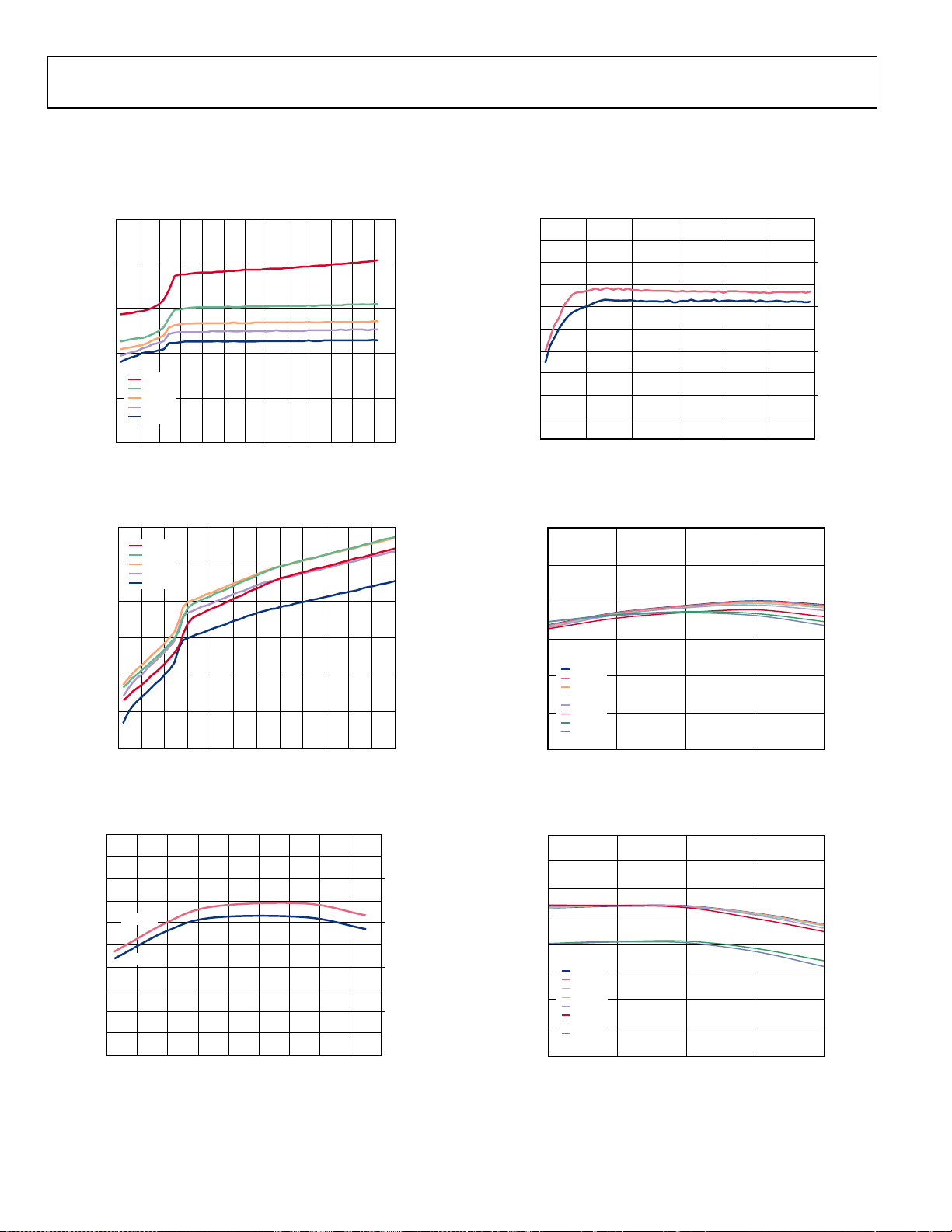
TYPICAL PERFORMANCE CHARACTERISTICS
BUCK OUTPUT
Using recommended inductor values, I
Figure 3. Quiescent Supply Current vs. Input Voltage, Nonswitching,
Different Temperatures
= 10 mA, CIN = C
OUT
= 10 µF, automatic PSM/PWM mode, TA = 25°C, unless otherwise noted.
OUT
Figure 6. Switching Frequency vs. Input Voltage, FPWM Mode
Figure 4. FPWM Quiescent Supply Current vs. Input Voltage, Nonswitching,
Different Temperatures
Figure 5. Switching Frequency vs. Temperature, FPWM Mode, VIN = 8 V
Figure 7. Output Voltage vs. Temperature, V
Different Loads
Figure 8. Output Voltage vs. Temperature, V
Different Loads
= 3.3 V, VIN = 7.3 V,
OUT
= 5 V, VIN = 7.2 V,
OUT
Rev. A | Page 8 of 32
Data Sheet ADP2370/ADP2371
1.15
1.17
1.19
1.21
1.23
1.25
–40 –5 25 85 125
OUTPUT VOLTAGE (V)
TEMPERATURE (°C)
0.1mA
1mA
5mA
10mA
50mA
100mA
300mA
800mA
09531-009
1.70
1.75
1.80
1.85
1.90
–40 –5 25 85 125
OUTPUT VOLTAGE (V)
TEMPERATURE (°C)
0.1mA
1m
A
5mA
10mA
50mA
100mA
300mA
800mA
09531-010
3.10
3.15
3.20
3.25
3.30
3.35
3.40
3 5 7 9 11 13 15
OUTPUT VOLTAGE (V)
INPUT VOLTAGE (V)
0.1mA
1mA
5mA
10mA
50mA
100mA
300mA
800mA
09531-011
3.10
3.15
3.20
3.25
3.30
3.35
3.40
0.1 1 10 100 1000
OUTPUT VOLTAGE (V)
LOAD (mA)
3.8V
4.55V
6.05V
7.30V
10.55V
12.05V
15.05V
09531-012
3.10
3.15
3.20
3.25
3.30
3.35
3.40
3 5 7 9 11 13 15
OUTPUT VOLTAGE (V)
INPUT VOLTAGE (V)
0.1mA
1mA
5mA
10mA
50mA
100mA
300mA
800mA
09531-013
4.80
4.85
4.90
4.95
5.00
5.05
5.10
5.15
5.20
0.1 1 10 100 1000
OUTPUT VOLTAGE (V)
LOAD (mA)
5.40V
6.00V
7.20V
9.00V
10.80V
12.00V
15.05V
09531-014
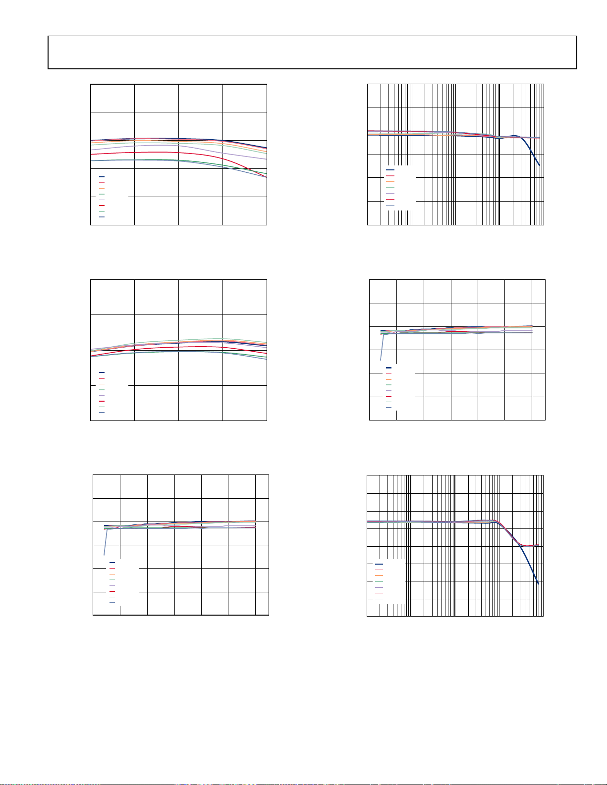
Figure 9. Output Voltage vs. Temperature, V
Different Loads
Figure 10. Output Voltage vs. Temperature, V
Different Loads
= 1.2 V, VIN = 4 V,
OUT
= 1.8 V, VIN = 7.2 V,
OUT
Figure 12. Load Regulation, V
Figure 13. Line Regulation, V
= 3.3 V
OUT
= 5.0 V, Different Loads
OUT
Figure 11. Line Regulation, V
= 3.3 V, Different Loads
OUT
Rev. A | Page 9 of 32
Figure 14. Load Regulation, V
OUT
= 5.0 V
ADP2370/ADP2371 Data Sheet
1.15
1.16
1.17
1.18
1.19
1.20
1.21
1.22
1.23
1.24
1.25
3 5 7 9 11 13 15
OUTPUT VOLTAGE (V)
INPUT VOLTAGE (V)
0.1mA
1mA
5mA
10mA
50mA
100mA
300mA
800mA
09531-015
1.15
1.16
1.17
1.18
1.19
1.20
1.21
1.22
1.23
1.24
1.25
0.1 1 10 100 1000
OUTPUT VOLTAGE (V)
LOAD (mA)
3.20V
3.95V
5.45V
7.20V
9.95V
11.95V
15.20V
09531-016
1.70
1.75
1.80
1.85
1.90
3 5 7 9 11 13 15
OUTPUT VOLTAGE (V)
INPUT VOLTAGE (V)
0.1mA
1mA
5mA
10mA
50mA
100mA
300mA
800mA
09531-017
1.70
1.75
1.80
1.85
1.90
0.1 1 10 100 1000
OUTPUT VOLTAGE (V)
LOAD (mA)
09531-018
3.20V
3.95V
5.45V
7.20V
9.95V
11.95V
15.20V
0
10
20
30
40
50
60
70
80
90
100
0.01 0.10 1.0 10 100 1000
EFFICIENCY (%)
LOAD (mA)
09531-019
3.80V
4.55V
6.05V
7.30V
10.55V
12.05V
15.05V
0
10
20
30
40
50
60
70
80
90
100
0.01 0.10 1.0 10 100 1000
EFFICIENCY (%)
LOAD (mA)
09531-020
–40°C
–5°C
+25°C
+85°C
+125°C
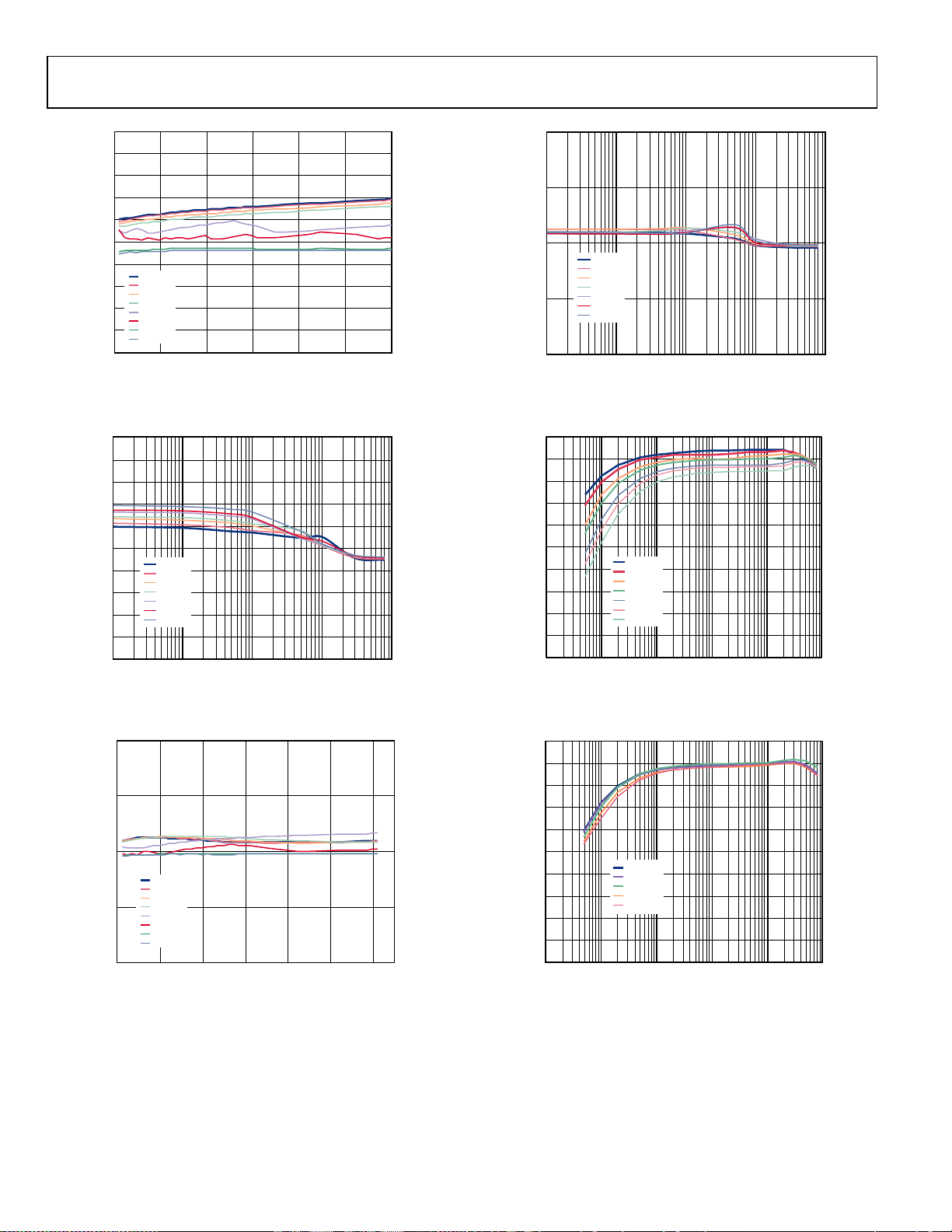
Figure 15. Line Regulation, V
Figure 16. Load Regulation, V
= 1.2 V, Different Loads
OUT
= 1.2 V
OUT
Figure 18. Load Regulation, V
Figure 19. Efficiency vs. Load Current, V
= 1.8 V
OUT
= 3.3 V, Different Input Voltages
OUT
Figure 17. Line Regulation, V
= 1.8 V, Different Loads
OUT
Figure 20. Efficiency vs. Load Current, V
V
= 3.3 V, Different Temperatures,
OUT
= 7.3 V
IN
Rev. A | Page 10 of 32
 Loading...