Regulator with Integrated High-Side MOSFET
ADP2325
Rev. 0
Information furnished by Analog Devices is believed to be accurate and reliable. However, no
Trademarks and registered trademarks are the property of their respective owners.
Fax: 781.461.3113 ©2012 Analog Devices, Inc. All rights reserved.
BST1
PVIN1
SW1
DL1
PGND
SW2
DL2
EN1
PGOOD1
SS1
COMP1
FB1
BST2
PVIN2
EN2
SS2
COMP2
FB2
PGOOD2
GND
SYNC
SCFG
INTVCC
RT
VDRV
V
OUT1
V
OUT2
V
IN
ADP2325
L1
L2
C
OUT1
C
OUT2
C
IN1
M1
M2
R
OSC
C
BST1
C
SS2
C
C2
R
C2
R
TOP1
R
BOT2
R
TOP2
C
INT
C
DRV
TRK1
TRK2
MODE
V
IN
C
IN2
C
BST2
R
BOT1
R
C1
C
C1
C
SS1
10036-001
50
55
60
65
70
75
80
85
90
95
100
0 1.0 2.0 3.0 4.00.5 1.5 2.5 3.5 4.5 5.0
EFFICIENCY (%)
OUTPUT CURRE NT (A)
V
OUT
= 5.0V
V
OUT
= 3.3V
10036-002
Data Sheet
FEATURES
Input voltage: 4.5 V to 20 V
±1% output accuracy
Integrated 48 mΩ typical high-side MOSFET
Flexible output configuration
Dual output: 5 A/5 A
Parallel single output: 10 A
Programmable switching frequency: 250 kHz to 1.2 MHz
External synchronization input with programmable phase
shift or internal clock output
Selectable PWM or PFM mode operation
Adjustable current limit for small inductors
External compensation and soft start
Startup into precharged output
Supported by ADIsimPower
APPLICATIONS
Communications infrastructure
Networking and servers
Industrial and instrumentation
Healthcare and medical
Intermediate power rail conversion
TM
design tool
Dual 5 A, 20 V Synchronous Step-Down
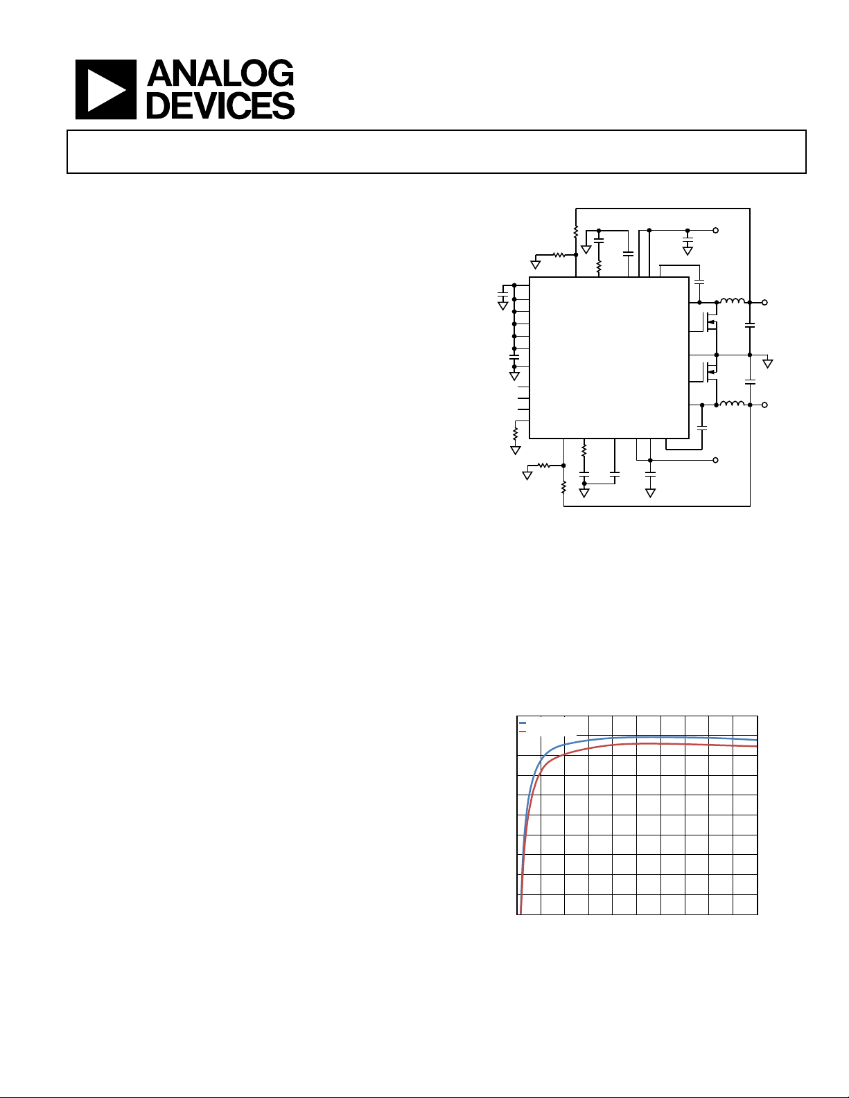
TYPICAL APPLICATION CIRCUIT
Figure 1.
GENERAL DESCRIPTION
The ADP2325 is a full featured, dual output, step-down dc-to-dc
regulator based on a current mode architecture. The ADP2325
integrates two high-side power MOSFETs and two low-side drivers
for the external N-channel MOSFETs. The two pulse-width modulation (PWM) channels can be configured to deliver dual 5 A
outputs or a parallel-to-single 10 A output. The regulator operates
from input voltages of 4.5 V to 20 V, and the output voltage can
be as low as 0.6 V.
The switching frequency can be programmed from 250 kHz to
1.2 MHz, or it can be synchronized to an external clock to
minimize interference in multirail applications. The dual PWM
channels run 180° out of phase, thereby reducing input current
ripple as well as reducing the size of the input capacitor.
The bidirectional synchronization pin can be programmed at
a 60°, 90°, or 120° phase shift to provide for a stackable, multiphase power solution.
The ADP2325 can be configured to operate in pulse frequency
modulation (PFM) mode at a light load for higher efficiency or
in forced PWM mode for noise sensitive applications. External
compensation and soft start provide design flexibility.
responsibility is assumed by Analog Devices for its use, nor for any infringements of patents or other
rights of third parties that may result from its use. Specifications subject to change without notice. No
license is granted by implication or otherwise under any patent or patent rights of Analog Devices.
Independent enable inputs and power-good outputs provide
reliable power sequencing. To enhance system reliability, the device
includes undervoltage lockout (UVLO), overvoltage protection
(OVP), overcurrent protection, and thermal shutdown.
The ADP2325 operates over the −40°C to +125°C junction
temperature range and is available in a 32-lead LFCSP_WQ
package.
One Technology Way, P.O. Box 9106, Norwood, MA 02062-9106, U.S.A.
Tel: 781.329.4700
Figure 2. Efficiency vs. Output Current at V
= 12 V, fSW = 600 kHz
IN
www.analog.com

ADP2325 Data Sheet
TABLE OF CONTENTS
Features .............................................................................................. 1
Applications ....................................................................................... 1
Typical Application Circuit ............................................................. 1
General Description ......................................................................... 1
Revision History ............................................................................... 2
Functional Block Diagram .............................................................. 3
Specifications ..................................................................................... 4
Absolute Maximum Ratings ....................................................... 6
Thermal Resistance ...................................................................... 6
ESD Caution .................................................................................. 6
Pin Configuration and Function Descriptions ............................. 7
Typical Performance Characteristics ............................................. 9
Theory of Operation ...................................................................... 16
Control Scheme .......................................................................... 16
PWM Mode ................................................................................. 16
PFM Mode ................................................................................... 16
Precision Enable/Shutdown ...................................................... 16
Separate Input Voltages ............................................................. 16
Internal Regulator (INTVCC) .................................................. 16
Bootstrap Circuitry .................................................................... 17
Low-Side Driver .......................................................................... 17
Oscillator ..................................................................................... 17
Synchronization .......................................................................... 17
Soft Start ...................................................................................... 17
Peak Current-Limit and Short-Circuit Protection ................. 17
Voltage Tracking ......................................................................... 18
Parallel Operation....................................................................... 18
Power Good ................................................................................. 19
Overvoltage Protection .............................................................. 19
Undervoltage Lockout ............................................................... 19
Thermal Shutdown .................................................................... 19
Applications Information .............................................................. 20
Input Capacitor Selection .......................................................... 20
Output Voltage Setting .............................................................. 20
Volta ge Conversion Limitations ............................................... 20
Current-Limit Setting ................................................................ 20
Inductor Selection ...................................................................... 20
Output Capacitor Selection....................................................... 21
Low-Side Power Device Selection ............................................ 22
Programming UVLO Input ...................................................... 22
Compensation Components Design ....................................... 22
Design Example .............................................................................. 24
Output Voltage Setting .............................................................. 24
Current-Limit Setting ................................................................ 24
Frequency Setting ....................................................................... 24
Inductor Selection ...................................................................... 24
Output Capacitor Selection....................................................... 24
Low-Side MOSFET Selection ................................................... 25
Compensation Components ..................................................... 25
Soft Start Time Programming .................................................. 26
Input Capacitor Selection .......................................................... 26
External Components Recommendations .................................. 27
Typical Application Circuits ......................................................... 28
Packaging and Ordering Information ......................................... 32
Outline Dimensions ................................................................... 32
Ordering Guide .......................................................................... 32
REVISION HISTORY
2/12—Revision 0: Initial Version
Rev. 0 | Page 2 of 32
Data Sheet ADP2325
+
–
+
0.6V
I
SS1
SS1
FB1
COMP1
Σ
AMP1
CONTROL
LOGIC
AND MOSFET
DRIVER WI TH
ANTICROSS
PROTECTION
BST1
SW1
I1
MAX
I1
MAX
HICCUP
MODE
NFET1
VDRV
DL1
0.7V
0.54V
OVP
PGOOD1
PVIN1
UVLO
EN1
CURRENT-
LIMIT
SELECTION
OSCILLATOR
PGND
SCFG
SYNC
RT
CLK1
CLK2
SLOPE RAMP1
SLOPE RAMP2
5V REGULAT OR
EN1_BUF
ADP2325
EN1_BUF
EN2_BUF
INTVCC
PVIN1
GND
MODE
MODE_BUF
SKIP MODE
THRESHOLD
MODE_BUF
SKIP
CMP1
SLOPE RAMP1
CLK1
–
+
VDRV
+
TRK1
+
–
+
–
1.2V
4µA1µA
OCP
CMP1
+
–
+
–
+
–
+
–
DRIVER
DRIVER
BOOST
REGULATOR
+
–
+
0.6V
I
SS2
SS2
FB2
COMP2
Σ
AMP2
CONTROL
LOGIC
AND MOSFET
DRIVER WI TH
ANTICROSS
PROTECTION
BST2
SW2
I2
MAX
I2
MAX
HICCUP
MODE
NFET2
VDRV
DL2
0.7V
0.54V
OVP
PGOOD2
PVIN2
UVLO
EN2
CURRENT-
LIMIT
SELECTION
EN2_BUF
SKIP MODE
THRESHOLD
MODE_BUF
SKIP
CMP2
SLOPE RAMP2
CLK2
–
+
LOW-SIDE
CURRENT
SENSE
+
TRK2
+
–
+
–
1.2V
4µA1µA
OCP
CMP2
+
–
+
–
+
–
+
–
DRIVER
DRIVER
BOOST
REGULATOR
A
CS1
A
CS2
10036-003
LOW-SIDE
CURRENT
SENSE
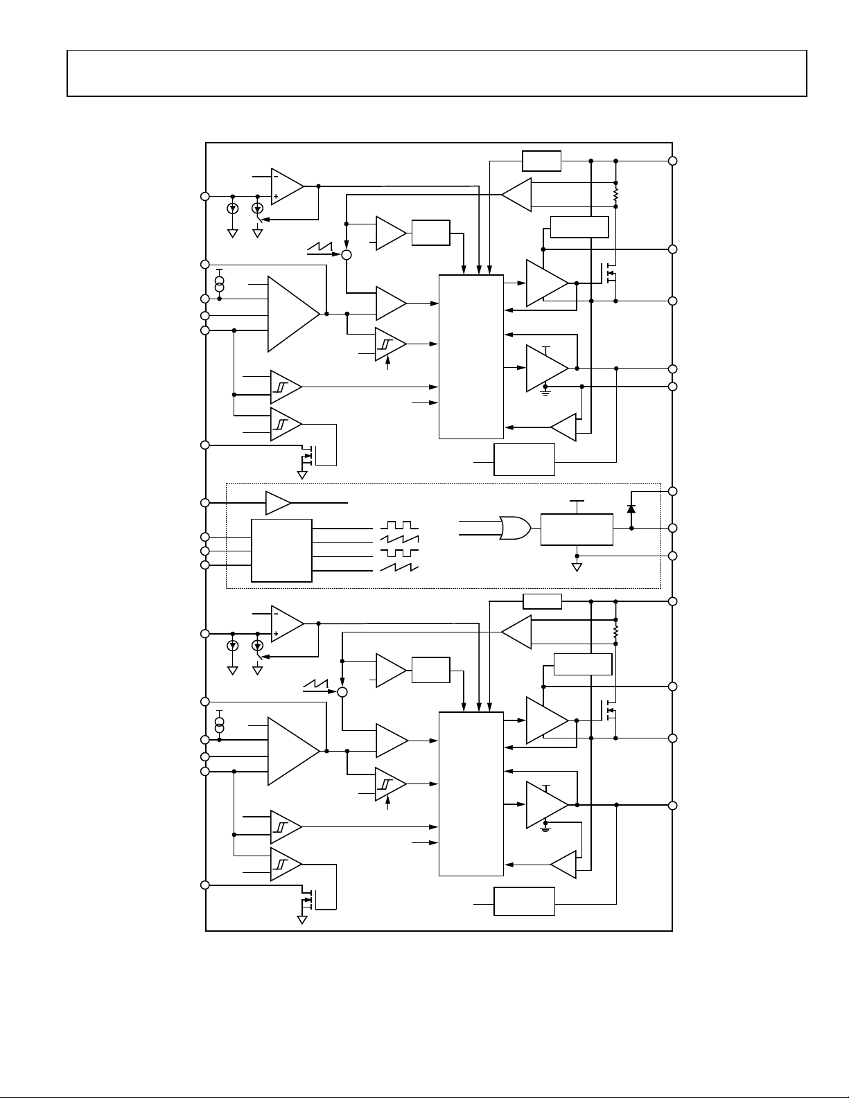
FUNCTIONAL BLOCK DIAGRAM
Rev. 0 | Page 3 of 32
Figure 3.

ADP2325 Data Sheet
SPECIFICATIONS
PVIN1 = PVIN2 = 12 V at TJ = −40°C to +125°C, unless otherwise noted.
Table 1.
Parameters Symbol Test Conditions/Comments Min Typ Max Unit
POWER INPUT (PVINx PINS)
Power Input Voltage Range V
Quiescent Current (PVIN1 + PVIN2) IQ MODE = GND, no switching 3 5 mA
Shutdown Current (PVIN1 + PVIN2) I
PVINx Undervoltage Lockout Threshold UVLO
PVINx Rising 4.2 4.4 V
PVINx Falling 3.5 3.7 V
FEEDBACK (FBx PINS)
FBx Regulation Voltage1 V
FBx Bias Current IFB 0.01 0.1 μA
ERROR AMPLIFIER (COMPx PINS)
Transconductance gm 370 500 630 μS
Error Amplifier Source Current I
Error Amplifier Sink Current I
INTERNAL REGULATOR (INTVCC PIN)
INTVCC Voltage 4.75 5 5.25 V
Dropout Voltage I
Regulator Current Limit 80 100 120 mA
SWITCH NODE (SWx PINS)
High-Side On Resistance2 V
High-Side Peak Current Limit R
R
Low-Side Negative Current-Limit Threshold
Voltage
3
SWx Minimum On Time3 t
SWx Minimum Off Time3 t
LOW-SIDE DRIVER (DLx PINS)
Rising Time3 t
Falling Time3 t
Sourcing Resistor 4 6 Ω
Sinking Resistor 1.4 3 Ω
OSCILLATOR (RT PIN)
PWM Switching Frequency fSW R
PWM Frequency Range 250 1200 kHz
SYNCHRONIZATION (SYNC PIN)
SYNC Input SYNC configured as input
Synchronization Range 300 1200 kHz
Minimum On Pulse Width 100 ns
Minimum Off Pulse Width 100 ns
High Threshold 1.3 V
Low Threshold 0.4 V
SYNC Output SYNC configured as output
Frequency on SYNC Pin f
Positive Pulse Time 100 ns
SOFT START (SSx PINS)
SSx Pin Source Current ISS 2.5 3.5 4.5 μA
4.5 20 V
PVIN
EN1 = EN2 = GND 30 40 μA
SHDN
PVINx = 4.5 V to 20 V 0.594 0.6 0.606 V
FB
40 65 90 μA
SOURCE
45 65 85 μA
SINK
= 30 mA 300 mV
INTVCC
to VSW = 5 V 48 80 mΩ
BST
= floating, V
ILIM
= 47 kΩ, V
ILIM
to VSW = 5 V 6.4 8 9.6 A
BST
to VSW = 5 V 3.4 4.8 6.2 A
BST
50 mV
130 ns
MIN_ON
150 ns
MIN_OFF
C
R
C
F
fSW kHz
CLKOUT
= 2.2 nF, see Figure 23 20 ns
DL
= 2.2 nF, see Figure 26 10 ns
DL
= 100 kΩ 510 600 690 kHz
OSC
Rev. 0 | Page 4 of 32

Data Sheet ADP2325
ENABLE (ENx PINS)
Parameters Symbol Test Conditions/Comments Min Typ Max Unit
TRACKING INPUT (TRKx PINS)
TRKx Input Voltage Range 0 600 mV
TRKx-to-FBx Offset Voltage TRKx = 0 mV to 500 mV −12 +12 mV
TRKx Input Bias Current 100 nA
POWER GOOD (PGOODx PINS)
Power-Good Rising Threshold 87 90 93 %
Power-Good Hysteresis 5 %
Power-Good Deglitch Time From FBx to PGOODx 16 Clock cycles
PGOODx Leakage Current V
PGOODx Output Low Voltage I
ENx Rising Threshold 1.2 1.28 V
ENx Falling Threshold 1.02 1.1 V
ENx Source Current EN voltage below falling
EN voltage above rising
MODE (MODE PIN)
Input High Voltage 1.3 V
Input Low Voltage 0.4 V
THERMAL SHUTDOWN
Thermal Shutdown Threshold 150 °C
Thermal Shutdown Hysteresis 15 °C
1
Tested in a feedback loop that adjusts VFB to achieve a specified voltage on the COMPx pin.
2
Pin-to-pin measurements.
3
Guaranteed by design.
= 5 V 0.1 1 µA
PGOOD
= 1 mA 50 100 mV
PGOOD
5 µA
threshold
1 µA
threshold
Rev. 0 | Page 5 of 32
ADP2325 Data Sheet
PVIN1, PVIN2, EN1, EN2
−0.3 V to +22 V
INTVCC, VDRV, DL1, DL2
−0.3 V to +6 V
Stresses a bove those listed under Absolut
e Maximum R atings
may cause permanent dam age to the device. This is a stress
rating only; functional operation of the device at these or any
other conditions above those indi cated in the operational
section of this specification is not implied. Exposure to absolute
maximum rating conditions for extended periods may affect
device reliability.
ABSOLUTE MAXIMUM RATINGS
Table 2.
Parameter Rating
SW1, SW2 −1 V to +22 V
BST1, BST2 VSW + 6 V
FB1, FB2, SS1, SS2, COMP1, COMP2,
PGOOD1, PGOOD2, TRK1, TRK2, SCFG,
SYNC, RT, MODE
PGND to GND −0.3 V to +0.3 V
Temperature Range
Operating (Junction) −40°C to +125°C
Storage −65°C to +150°C
Soldering Conditions JEDEC J-STD-020
−0.3 V to +6 V
THERMAL RESISTANCE
θJA is specified for the worst-case conditions, that is, a device
soldered in a circuit board for surface-mount packages.
Boundary Condition
θJA is measured using natural convection on a JEDEC 4-layer
board, and the exposed pad is soldered to the printed circuit
board (PCB) with thermal vias.
Table 3. Thermal Resistance
Package Type θJA Unit
32-Lead LFCSP_WQ 32.7 °C/W
ESD CAUTION
Rev. 0 | Page 6 of 32

Data Sheet ADP2325
PIN CONFIGURATION AND FUNCTION DESCRIPTIONS
FB1
COMP1
SS1
TRK1
EN1
PVIN1
PVIN1
SW1
32313029282726
1SW1
PGOOD1
2
SCFG
SYNC
3
4
5
6
7
8
ADP2325
TOP VIEW
(Not to Scale)
9
10111213141516
FB2
SS2
TRK2
COMP2
GND
INTVCC
RT
MODE
PGOOD2
NOTES
1. THE EXPOSEDPAD SHOULD BE SOLDERED
TO AN EXTERNAL GND PLANE.
Figure 4. Pin Configuration (Top View)
Table 4. Pin Function Descriptions
Pin No. Mnemonic Description
1 PGOOD1 Power-Good Output (Open Drain) for Channel 1. A pull-up resistor of 10 kΩ to 100 kΩ is recommended.
2 SCFG
Synchronization Configuration Input. The SCFG pin configures the SYNC pin as an input or an output. Connect
SCFG to INTVCC to configure SYNC as an output. Connecting a pull-down resistor to GND configures SYNC as an
input with various phase shift degrees.
3 SYNC
Synchronization. This pin can be configured as an input or an output. When configured as an output, it provides a
clock at the switching frequency. When configured as an input, this pin accepts an external clock to which the
regulators are synchronized. The phase shift is configured by SCFG. Note that when SYNC is configured as an input,
the PFM mode is disabled and the device works in continuous conduction mode (CCM) only.
4 GND Analog Ground. Connect to the ground plane.
5 INTVCC
Internal 5 V Regulator Output. The IC control circuits are powered from this voltage. Place a 1 F ceramic capacitor
between INTVCC and GND.
6 RT Connect a resistor between RT and GND to program the switching frequency from 250 kHz to 1.2 MHz.
7 MODE
Mode Selection. When this pin is connected to INTVCC, the PFM mode is disabled and the regulator works only in
CCM. When this pin is connected to ground, the PFM mode is enabled. If the low-side device is a diode, the MODE
pin must be connected to ground.
8 PGOOD2 Power-Good Output (Open Drain) for Channel 2. A pull-up resistor of 10 kΩ to 100 kΩ is recommended.
9 FB2
10 COMP2
Feedback Voltage Sense Input for Channel 2. Connect FB2 to a resistor divider from the Channel 2 output voltage,
V
. Connect FB2 to INTVCC for parallel applications.
OUT2
Error Amplifier Output for Channel 2. Connect an RC network from COMP2 to GND. Connect COMP1 and COMP2
together for parallel applications.
11 SS2
Soft Start Control for Channel 2. To program the soft start time, connect a capacitor from SS2 to GND. For parallel
applications, SS2 remains open.
12 TRK2
Tracking Input for Channel 2. To track a master voltage, connect this pin to a resistor divider from the master
voltage. If the tracking function is not used, connect TRK2 to INTVCC.
13 EN2
Enable Pin for Channel 2. An external resistor divider can be used to set the turn-on threshold. When not using the
enable pin, connect EN2 to PVIN2.
14, 15 PVIN2
Power Input for Channel 2. Connect PVIN2 to the input power source, and connect a bypass capacitor between
PVIN2 and ground.
16, 17 SW2 Switch Node for Channel 2.
18 BST2 Supply Rail for the Gate Drive of Channel 2. Place a 0.1 µF capacitor between SW2 and BST2.
19 DL2
Low-Side Gate Driver Output for Channel 2. Connect a resistor between DL2 and PGND to program the current-
limit threshold of Channel 2.
20 VDRV Low-Side Driver Supply Input. Connect VDRV to INTVCC. Place a 1 µF ceramic capacitor between the VDRV pin and PGND.
21 PGND Driver Power Ground. Connect to the source of the synchronous N-channel MOSFET.
22 DL1
Low-Side Gate Driver Output for Channel 1. Connect a resistor between DL1 and PGND to program the current-
limit threshold of Channel 1.
23 BST1 Supply Rail for the Gate Drive of Channel 1. Place a 0.1 µF capacitor between SW1 and BST1.
25
24
23
BST1
DL1
22
PGND
21
20
VDRV
19
DL2
18
BST2
SW2
17
EN2
SW2
PVIN2
PVIN2
10036-004
Rev. 0 | Page 7 of 32

ADP2325 Data Sheet
Pin No. Mnemonic Description
24, 25 SW1 Switch Node for Channel 1.
26, 27 PVIN1
28 EN1
29 TRK1
30 SS1 Soft Start Control for Channel 1. To program the soft start time, connect a capacitor from SS1 to GND.
31 COMP1
32 FB1 Feedback Voltage Sense Input for Channel 1. Connect FB1 to a resistor divider from the Channel 1 output voltage, V
N/A1 EP Exposed Pad. Solder the exposed pad to an external GND plane.
1
N/A means not applicable.
Power Input for Channel 1. These pins are the power inputs for Channel 1 and provide power for the internal
regulator. Connect to the input power source and connect a bypass capacitor between PVIN1 and ground.
Enable Pin for Channel 1. An external resistor divider can be used to set the turn-on threshold. When not using
the enable pin, connect EN1 to PVIN1.
Tracking Input for Channel 1. To track a master voltage, connect this pin to a resistor divider from the master
voltage. If the tracking function is not used, connect TRK1 to INTVCC.
Error Amplifier Output for Channel 1. Connect an RC network from COMP1 to GND. Connect COMP1 and COMP2
together for parallel applications.
OUT1
.
Rev. 0 | Page 8 of 32
Data Sheet ADP2325
50
55
60
65
70
75
80
85
90
95
100
0 0.5 1.0 1.5 2.0 2.5 3.0 3.5 4.0 4.5 5.0
EFFICIENCY (%)
OUTPUT CURRE NT (A)
INDUCTOR: FDVE1040-2R2M
MOSFET: FDS8880
V
OUT
= 5.0V
V
OUT
= 3.3V
V
OUT
= 2.5V
V
OUT
= 1.8V
V
OUT
= 1.5V
V
OUT
= 1.2V
10036-005
EFFICIENCY (%)
OUTPUT CURRENT (A)
0
10
20
30
40
50
60
70
80
90
100
0.01 0.1 1
INDUCTOR: F DV E 1040- 2R2M
MOSFET: FDS8880
V
OUT
= 5.0V, FPWM
V
OUT
= 3.3V, FPWM
V
OUT
= 5.0V, PFM
V
OUT
= 3.3V, PFM
10036-006
50
55
60
65
70
75
80
85
90
95
100
EFFICIENCY (%)
0 0.5 1.0 1.5 2.0 2.5 3.0 3.5 4.0 4.5 5.0
OUTPUT CURRE NT (A)
INDUCTOR: FDVE1040-1R5M
MOSFET: FDS8880
V
OUT
= 3.3V
V
OUT
= 2.5V
V
OUT
= 1.8V
V
OUT
= 1.5V
V
OUT
= 1.2V
10036-007
EFFICIENCY (%)
0 0.5 1.0 1.5 2.0 2.5 3.0 3.5 4.0 4.5 5.0
OUTPUT CURRE NT (A)
50
55
60
65
70
75
80
85
90
95
100
INDUCTOR: FDVE1040-4R7M
MOSFET: FDS8880
V
OUT
= 5.0V
V
OUT
= 3.3V
V
OUT
= 2.5V
V
OUT
= 1.8V
V
OUT
= 1.5V
V
OUT
= 1.2V
10036-008
0
10
20
30
40
50
60
70
80
90
100
0.01 0.1 1
EFFICIENCY (%)
OUTPUT CURRE NT (A)
V
OUT
= 5.0V, FPWM
V
OUT
= 3.3V, FPWM
V
OUT
= 5.0V, PFM
V
OUT
= 3.3V, PFM
INDUCTOR: FDVE1040-4R7M
MOSFET: FDS8880
10036-009
EFFICIENCY (%)
0 0.5 1.0 1.5 2.0 2.5 3.0 3.5 4.0 4.5 5.0
OUTPUT CURRE NT (A)
50
55
60
65
70
75
80
85
90
95
100
INDUCTOR: FDVE1040-4R7M
MOSFET: FDS8880
V
OUT
= 5.0V
V
OUT
= 3.3V
V
OUT
= 2.5V
V
OUT
= 1.8V
V
OUT
= 1.5V
V
OUT
= 1.2V
10036-010
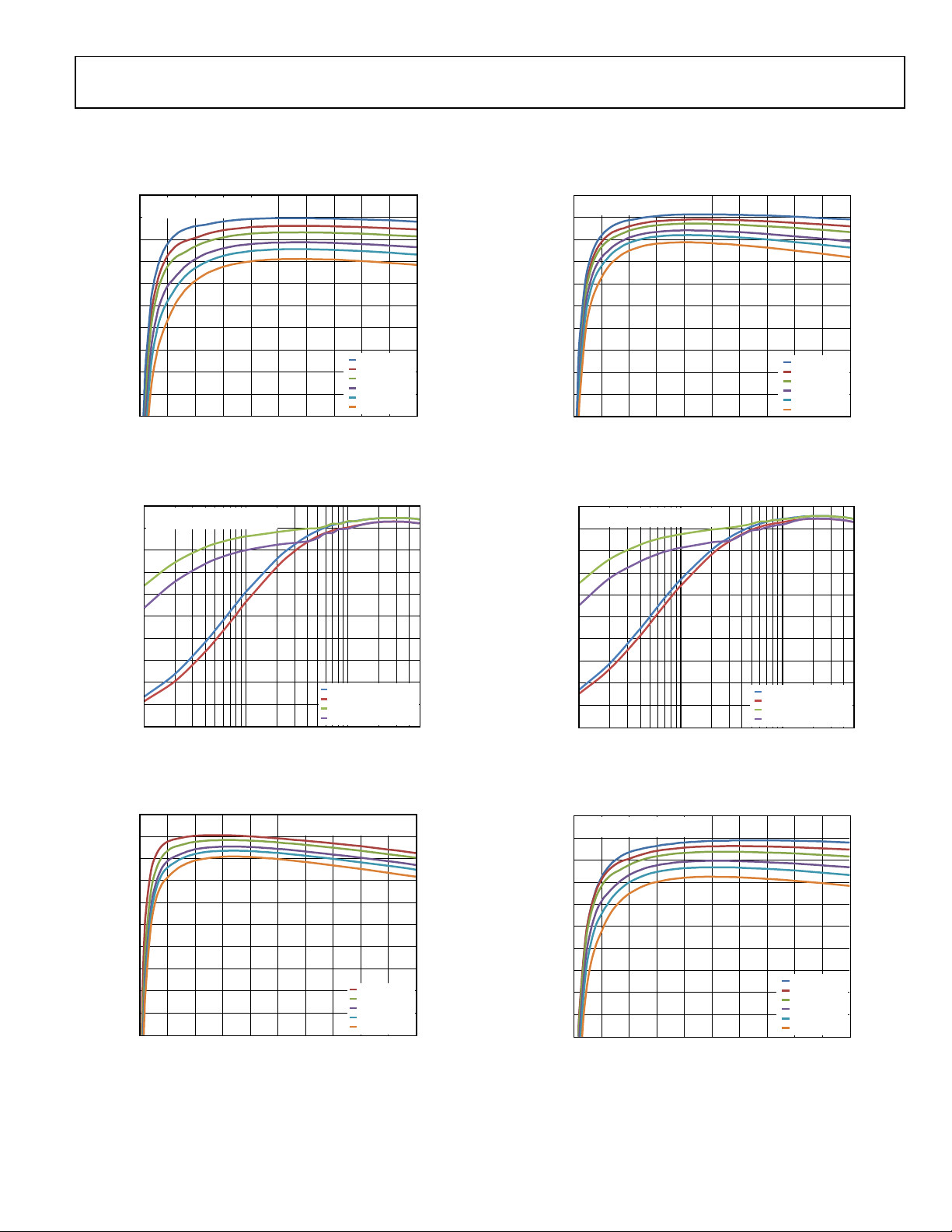
TYPICAL PERFORMANCE CHARACTERISTICS
TA = 25°C, VIN = 12 V, V
Figure 5. Efficiency at V
= 3.3 V, L = 2.2 µH, C
OUT
= 12 V, fSW = 600 kHz, FPWM
IN
= 2 × 100 µF, fSW = 600 kHz, unless otherwise noted.
OUT
Figure 8. Efficiency at VIN = 12 V, fSW = 300 kHz, FPWM
Figure 6. Efficiency at VIN = 12 V, fSW = 600 kHz, FPWM and PFM
Figure 7. Efficiency at VIN = 5 V, fSW = 600 kHz, FPWM
Figure 9. Efficiency at VIN = 12 V, fSW = 300 kHz, FPWM and PFM
Figure 10. Efficiency at VIN = 18 V, fSW = 300 kHz, FPWM
Rev. 0 | Page 9 of 32
ADP2325 Data Sheet
10
15
20
25
30
35
40
4 6 8 10 12 14 16 18 20
SHUTDOWN CURRE NT (μA)
T
J
= –40°C
TJ = +25°C
T
J
= +125°C
V
IN
(V)
10036-011
3.5
3.6
3.7
3.8
3.9
4.0
4.1
4.2
4.3
4.4
4.5
–40 –20 0 20 40 60 80 100 120
UVLO THRES HOLD (V)
RISING
FALLING
TEMPERATURE (°C)
10036-012
0.90
0.92
0.94
0.96
0.98
1.00
1.02
1.04
1.06
1.08
1.10
–40 –20 0 20 40 60 80 100 120
EN SOURCE CURRENT ( µA)
TEMPERATURE (°C)
10036-013
2.80
2.85
2.90
2.95
3.00
3.05
3.10
4 6 8 10 12 14 16 18 20
QUIESCENT CURRE NT (mA)
VIN (V)
T
J
= –40°C
T
J
= +25°C
T
J
= +125°C
10036-014
1.00
1.05
1.10
1.15
1.20
1.25
1.30
–40 –20 0 20 40 60 80 100 120
ENABLE THRESHOLD (V)
RISING
FALLING
TEMPERATURE (°C)
10036-015
4.70
4.75
4.80
4.85
4.90
4.95
5.00
5.05
5.10
5.15
5.20
5.25
5.30
–40 –20 0 20 40 60 80 100 120
EN SOURCE CURRENT ( µA)
TEMPERATURE (°C)
10036-016
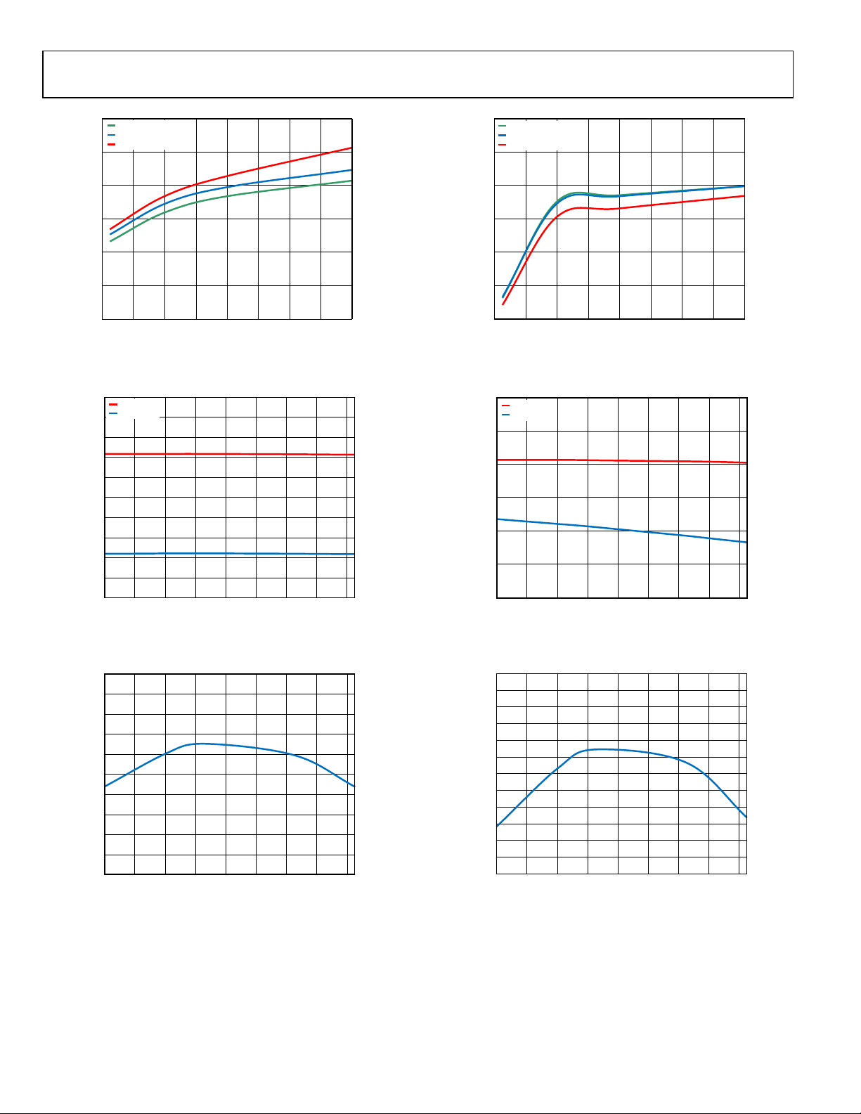
Figure 11. Shutdown Current vs. VIN
Figure 12. UVLO Threshold vs. Temperature
Figure 14. Quiescent Current vs. VIN
Figure 15. EN Threshold vs. Temperature
Figure 13. EN Source Current vs. Temperature at VEN = 1.5 V
Figure 16. EN Source Current vs. Temperature at VEN = 1 V
Rev. 0 | Page 10 of 32
 Loading...