

1.2 A, 20 V, 700 kHz/1.4 MHz,
C
Nonsynchronous Step-Down Regulator
FEATURES
1.2 A maximum load current
±2% output accuracy over temperature range
Wide input voltage range: 3.0 V to 20 V
700 kHz (ADP2300) or 1.4 MHz (ADP2301)
switching frequency options
High efficiency up to 91%
Current-mode control architecture
Output voltage from 0.8 V to 0.85 × V
Automatic PFM/PWM mode switching
Precision enable pin with hysteresis
Integrated high-side MOSFET
Integrated bootstrap diode
Internal compensation and soft start
Minimum external components
Undervoltage lockout (UVLO)
Overcurrent protection (OCP) and thermal shutdown (TSD)
ADIsimPower™ online design tool
Available in ultrasmall, 6-lead TSOT package
APPLICATIONS
LDO replacement for digital load applications
Intermediate power rail conversion
Communications and networking
Industrial and instrumentation
Healthcare and medical
Consumer
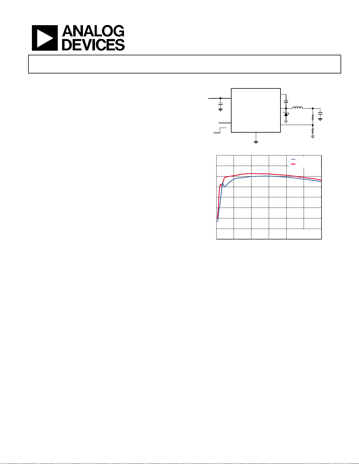
IN
ADP2300/ADP2301
TYPICAL APPLICATIONS CIRCUIT
Figure 1.
I
(A)
OUT
BST
SW
FB
f
SW
f
SW
3.0V TO 20V
OFF
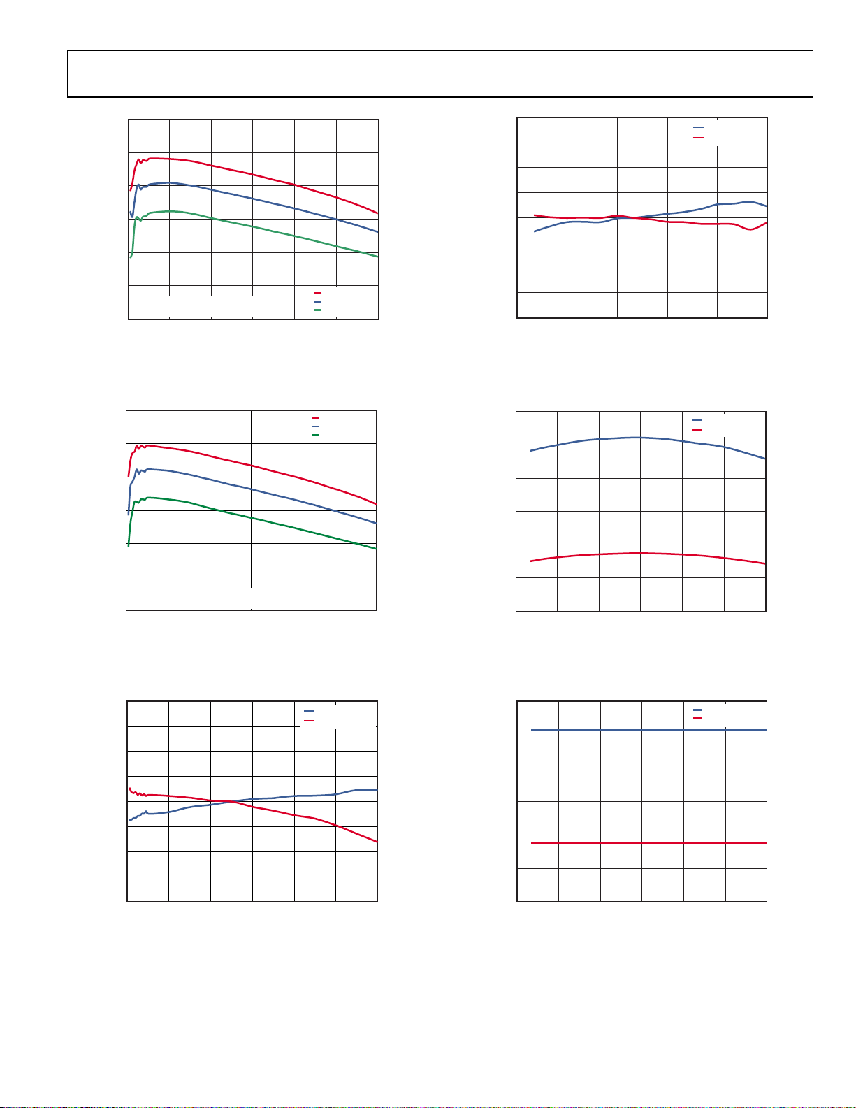
100
95
90
85
Y (%)
80
75
EFFICIEN
70
65
60
0 0.2 0.4 0.6 0.8 1.0 1.2
VIN
ADP2300/
ADP2301
EN
ON
Figure 2. Efficiency vs. Output Current
GND
= 1.4MHz
= 700kHz
V
= 12V
IN
V
OUT
V
= 5.0V
OUT
08342-001
08342-069
GENERAL DESCRIPTION
The ADP2300/ADP2301 are compact, constant-frequency,
current-mode, step-down dc-to-dc regulators with integrated
power MOSFET. The ADP2300/ADP2301 devices run from
input voltages of 3.0 V to 20 V, making them suitable for a wide
range of applications. A precise, low voltage internal reference
makes these devices ideal for generating a regulated output
voltage as low as 0.8 V, with ±2% accuracy, for up to 1.2 A load
current.
There are two frequency options: the ADP2300 runs at 700 kHz,
and the ADP2301 runs at 1.4 MHz. These options allow users to
make decisions based on the trade-off between efficiency and
Rev. A
Information furnished by Analog Devices is believed to be accurate and reliable. However, no
responsibility is assumed by Analog Devices for its use, nor for any infringem ents of patents or other
rights of third parties that may result from its use. Specifications subject to change without notice. No
license is granted by implication or otherwise under any patent or patent rights of Analog Devices.
Trademarks and registered trademarks are the property of their respective owners.
total solution size. Current-mode control provides fast and stable
line and load transient performance. The ADP2300/ADP2301
devices include internal soft start to prevent inrush current at
power-up. Other key safety features include short-circuit protection, thermal shutdown (TSD), and input undervoltage lockout
(UVLO). The precision enable pin threshold voltage allows the
ADP2300/ADP2301 to be easily sequenced from other input/
output supplies. It can also be used as a programmable UVLO
input by using a resistive divider.
The ADP2300/ADP2301 are available in a 6-lead TSOT package
and are rated for the −40°C to +125°C junction temperature range.
One Technology Way, P.O. Box 9106, Norwood, MA 02062-9106, U.S.A.
Tel: 781.329.4700 www.analog.com
Fax: 781.461.3113 ©2010 Analog Devices, Inc. All rights reserved.

ADP2300/ADP2301
TABLE OF CONTENTS
Features .............................................................................................. 1
Applications ....................................................................................... 1
Typical Applications Circuit ............................................................ 1
General Description ......................................................................... 1
Revision History ............................................................................... 2
Specifications ..................................................................................... 3
Absolute Maximum Ratings ............................................................ 4
Thermal Resistance ...................................................................... 4
ESD Caution .................................................................................. 4
Pin Configuration and Function Descriptions ............................. 5
Typical Performance Characteristics ............................................. 6
Functional Block Diagram ............................................................ 13
Theory of Operation ...................................................................... 14
Basic Operation .......................................................................... 14
PWM Mode ................................................................................. 14
Power Saving Mode .................................................................... 14
Bootstrap Circuitry .................................................................... 14
Precision Enable ......................................................................... 14
Integrated Soft Start ................................................................... 14
Current Limit .............................................................................. 14
Short-Circuit Protection ............................................................ 15
Undervoltage Lockout (UVLO) ............................................... 15
Thermal Shutdown .................................................................... 15
Control Loop ............................................................................... 15
Applications Information .............................................................. 16
Programming the Output Voltage ........................................... 16
Voltage Conversion Limitations ............................................... 16
Low Input Voltage Considerations .......................................... 17
Programming the Precision Enable ......................................... 17
Inductor ....................................................................................... 18
Catch Diode ................................................................................ 19
Input Capacitor ........................................................................... 19
Output Capacitor........................................................................ 19
Thermal Considerations ............................................................ 20
Design Example .............................................................................. 21
Switching Frequency Selection ................................................. 21
Catch Diode Selection ............................................................... 21
Inductor Selection ...................................................................... 21
Output Capacitor Selection....................................................... 21
Resistive Voltage Divider Selection .......................................... 22
Circuit Board Layout Recommendations ................................... 23
Typical Application Circuits ......................................................... 24
Outline Dimensions ....................................................................... 26
Ordering Guide .......................................................................... 26
REVISION HISTORY
6/10—Rev. 0 to Rev. A
Changes to Figure 54 ...................................................................... 25
Changes to Ordering Guide .......................................................... 26
2/10—Revision 0: Initial Version
Rev. A | Page 2 of 28

ADP2300/ADP2301
SPECIFICATIONS
VIN = 3.3 V, TJ = −40°C to +125°C for minimum/maximum specifications, and TA = 25°C for typical specifications, unless otherwise noted.
Table 1.
Parameter Symbol Test Conditions Min Typ Max Unit
VIN
Voltage Range VIN 3 20 V
Supply Current I
Shutdown Current I
Undervoltage Lockout Threshold UVLO VIN rising 2.80 2.95 V
V
FB
Regulation Voltage VFB T
T
Bias Current IFB 0.01 0.1 μA
SW
On Resistance1 V
Peak Current Limit2 V
Minimum On Time 100 135 ns
Minimum Off Time ADP2300 145 190 ns
ADP2301 70 120 ns
OSCILLATOR FREQUENCY ADP2300 0.5 0.7 0.9 MHz
ADP2301 1.0 1.4 1.75 MHz
SOFT START TIME ADP2300 1460 μs
ADP2301 730 μs
EN
Input Threshold VEN 1.13 1.2 1.27 V
Input Hysteresis 100 mV
Pull-Down Current 1.2 μA
BOOTSTRAP VOLTAGE V
THERMAL SHUTDOWN
Threshold 140 °C
Hysteresis 15 °C
1
Pin-to-pin measurements.
2
Guaranteed by design.
No switching, VIN = 12 V 640 800 μA
VIN
VEN = 0 V, VIN = 12 V 18 35 μA
SHDN
falling 2.15 2.40 V
IN
= 0°C to +125°C 0.788 0.800 0.812 V
J
= −40°C to +125°C 0.784 0.800 0.816 V
J
− VSW = 5 V, ISW = 150 mA 440 700 mΩ
BST
− VSW = 5 V, VIN = 12 V 1.5 1.9 2.5 A
BST
No switching, VIN = 12 V 5.0 V
BOOT
Rev. A | Page 3 of 28
ADP2300/ADP2301
ABSOLUTE MAXIMUM RATINGS
Table 2.
Parameter Rating
VIN, EN −0.3 V to +28 V
SW −1.0 V to +28 V
BST to SW −0.6 V to +6 V
BST −0.3 V to +28 V
FB −0.3 V to +3.3 V
Operating Junction Temperature Range −40°C to +125°C
Storage Temperature Range −65°C to +150°C
Soldering Conditions JEDEC J-STD-020
Stresses above those listed under Absolute Maximum Ratings
may cause permanent damage to the device. This is a stress
rating only; functional operation of the device at these or any
other conditions above those indicated in the operational
section of this specification is not implied. Exposure to absolute
maximum rating conditions for extended periods may affect
device reliability.
Absolute maximum ratings apply individually only, not in
combination. Unless otherwise specified, all voltages are
referenced to GND.
THERMAL RESISTANCE
θJA is specified for the worst-case conditions, that is, a device
soldered in a circuit board for surface-mount packages.
Table 3. Thermal Resistance
Package Type θJA θ
6-Lead TSOT 186.02 66.34 °C/W
1
θJA and θJC are measured using natural convection on a JEDEC 4-layer board.
1
Unit
JC
ESD CAUTION
Rev. A | Page 4 of 28
ADP2300/ADP2301
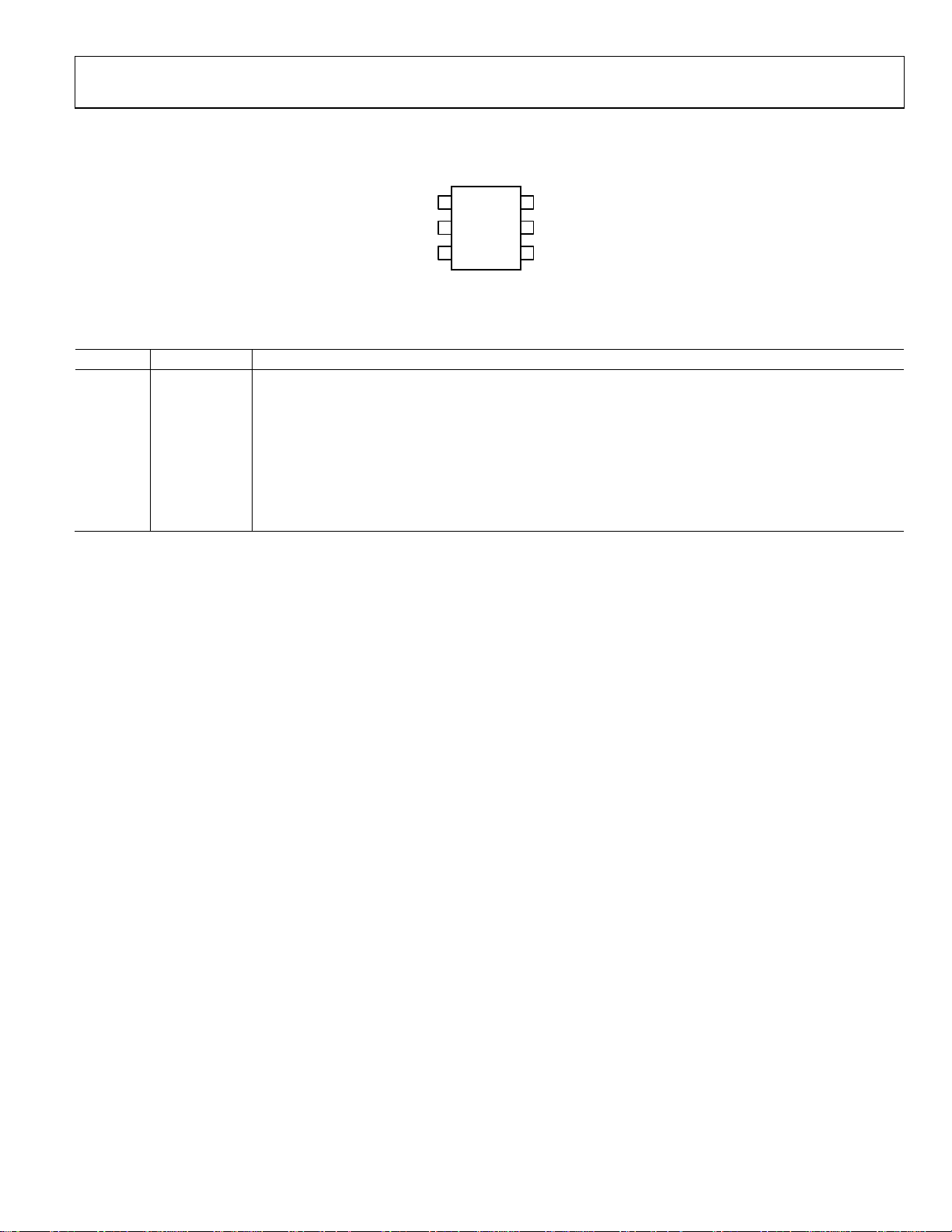
PIN CONFIGURATION AND FUNCTION DESCRIPTIONS
BST
GND
FB
1
ADP2300/
ADP2301
2
TOP VIEW
(Not to Scale)
3
6
SW
5
VIN
4
EN
08342-002
Figure 3. Pin Configuration
Table 4. Pin Function Descriptions
Pin No. Mnemonic Description
1 BST
Boost Supply for the High-Side MOSFET Driver. A 0.1 μF capacitor is connected between the SW and BST pins
to form a floating supply to drive the gate of the MOSFET switch above the VIN supply voltage.
2 GND Ground. Connect this pin to the ground plane.
3 FB
4 EN
Feedback Voltage Sense Input. Connect this pin to a resistive divider from V
desired V
OUT
.
Output Enable. Pull this pin high to enable the output. Pull this pin low to disable the output. This pin can
. Set the voltage to 0.8 V for a
OUT
also be used as a programmable UVLO input. This pin has a 1.2 μA pull-down current to GND.
5 VIN Power Input. Connect to the input power source with a ceramic bypass capacitor to GND directly from this pin.
6 SW Switch Node Output. Connect an inductor to V
and a catch diode to GND from this pin.
OUT
Rev. A | Page 5 of 28
ADP2300/ADP2301
C
C
C
C
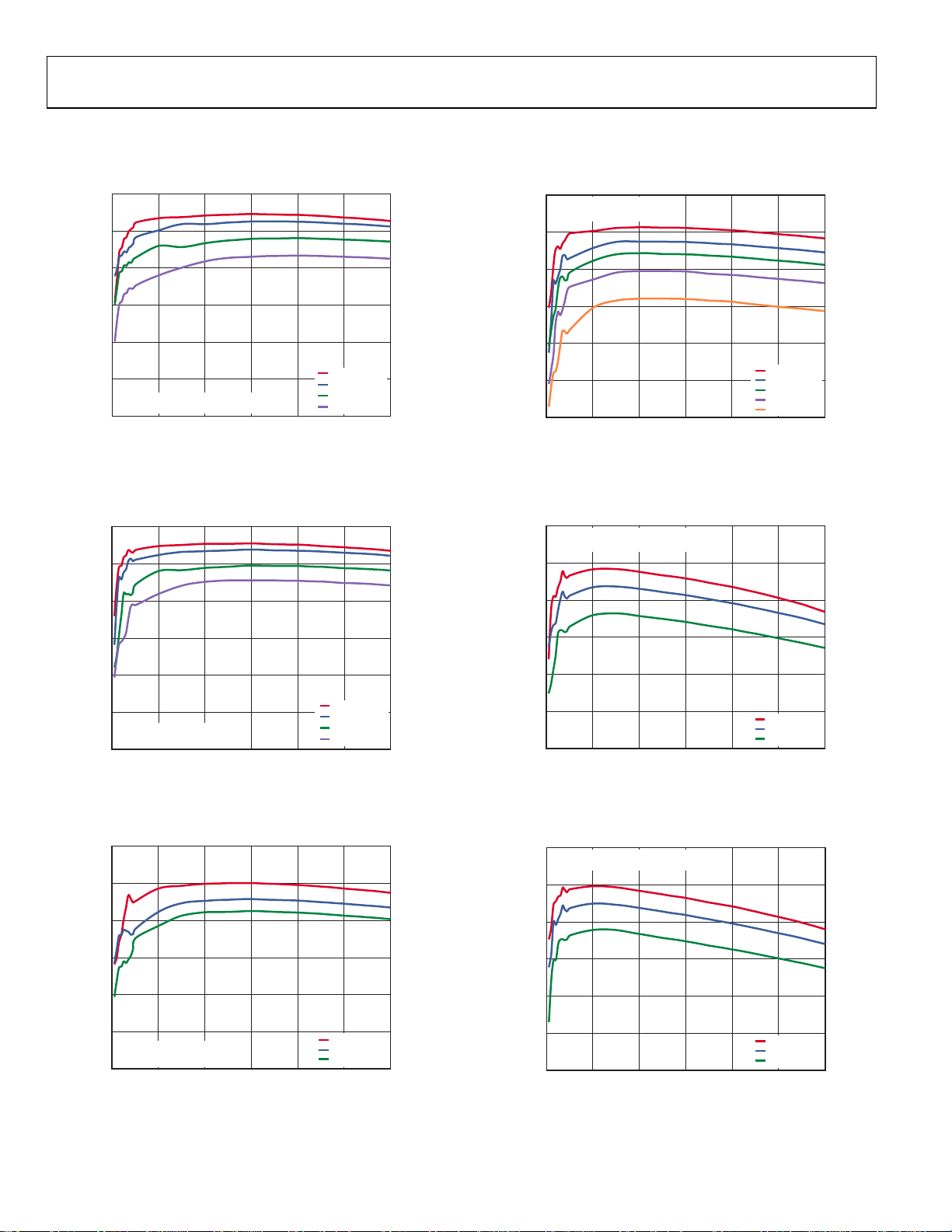
TYPICAL PERFORMANCE CHARACTERISTICS
VIN = 3.3 V, TA = 25°C, VEN = VIN, unless otherwise noted.
100
90
100
INDUCTOR: LPS6225-103MLC
DIODE: B230A
90
80
70
EFFICIENCY (%)
60
50
INDUCTOR: L PS6225-472MLC
DIODE: B230A
40
0 0.2 0.4 0.6 0.8 1.0 1.2
I
(A)
OUT
V
V
V
V
Figure 4. Efficiency Curve, VIN = 18 V, fSW = 1.4 MHz
100
90
80
Y (%)
70
EFFICIEN
60
50
INDUCTOR: L PS6225-103MLC
DIODE: B230A
40
0 0.2 0.4 0.6 0.8 1.0 1.2
I
(A)
OUT
Figure 5. Efficiency Curve, VIN = 18 V, fSW = 700 kHz
80
Y (%)
70
EFFICIEN
60
V
= 5.0V
OUT
OUT
OUT
OUT
= 12V
= 9V
= 5.0V
= 3.3V
50
40
0 0.2 0.4 0.6 0.8 1.0 1.2
I
08342-070
OUT
(A)
OUT
V
= 3.3V
OUT
V
= 2.5V
OUT
V
= 1.8V
OUT
V
= 1.2V
OUT
8342-073
Figure 7. Efficiency Curve, VIN = 12 V, fSW = 700 kHz
100
INDUCTOR: L PS6225-472MLC
DIODE: B230A
90
80
Y (%)
70
EFFICIEN
60
V
= 12V
OUT
V
= 9V
OUT
V
= 5.0V
OUT
V
= 3.3V
OUT
08342-071
50
40
0 0.2 0.4 0.6 0.8 1.0 1.2
I
(A)
OUT
V
= 2.5V
OUT
V
= 1.8V
OUT
V
= 1.2V
OUT
08342-074
Figure 8. Efficiency Curve, VIN = 5.0 V, fSW = 1.4 MHz
100
90
80
Y (%)
70
EFFICIEN
60
50
INDUCTOR: LPS6225-472MLC
DIODE: B230A
40
0 0.2 0.4 0.6 0.8 1.0 1.2
I
(A)
OUT
Figure 6. Efficiency Curve, VIN = 12 V, fSW = 1.4 MHz
V
= 5.0V
OUT
V
= 3.3V
OUT
V
= 2.5V
OUT
08342-072
100
INDUCTOR: L PS6225-103MLC
DIODE: B230A
90
80
70
EFFICIENCY (%)
60
50
40
0 0.2 0.4 0.6 0.8 1.0 1.2
I
(A)
OUT
Figure 9. Efficiency Curve, VIN = 5.0 V, fSW = 700 kHz
V
= 2.5V
OUT
= 1.8V
V
OUT
= 1.2V
V
OUT
08342-075
Rev. A | Page 6 of 28
ADP2300/ADP2301
A
A
C
C
100
90
80
70
EFFICIENCY (%)
60
50
INDUCTOR: L PS6225-472MLC
DIODE: B230A
40
0 0.2 0.4 0.6 0.8 1.0 1.2
I
(A)
OUT
V
= 1.8V
OUT
V
= 1.2V
OUT
V
= 0.8V
OUT
Figure 10. Efficiency Curve, VIN = 3.3 V with External 5.0 V Bootstrap Bias
Voltage, f
= 1.4 MHz
SW
08342-089
0.20
0.15
0.10
0.05
TION (%)
0
–0.05
LINE REGUL
–0.10
–0.15
–0.20
5 8 11 14 17 20
VIN (V)
Figure 13. Line Regulation, V
= 3.3 V, I
OUT
f
SW
f
SW
= 500 mA
OUT
= 1.4MHz
= 700kHz
8342-068
100
90
80
70
EFFICIENCY (%)
60
50
INDUCTOR: LPS6225-103MLC
DIODE: B230A
40
0 0.2 0.4 0.6 0.8 1.0 1.2
(A)
I
OUT
V
= 1.8V
OUT
V
= 1.2V
OUT
V
= 0.8V
OUT
Figure 11. Efficiency Curve, VIN = 3.3 V with External 5.0 V Bootstrap Bias
Voltage, f
0.20
0.15
0.10
0.05
TION (%)
0
= 700 kHz
SW
FSW = 1.4MHz
F
= 700kHz
SW
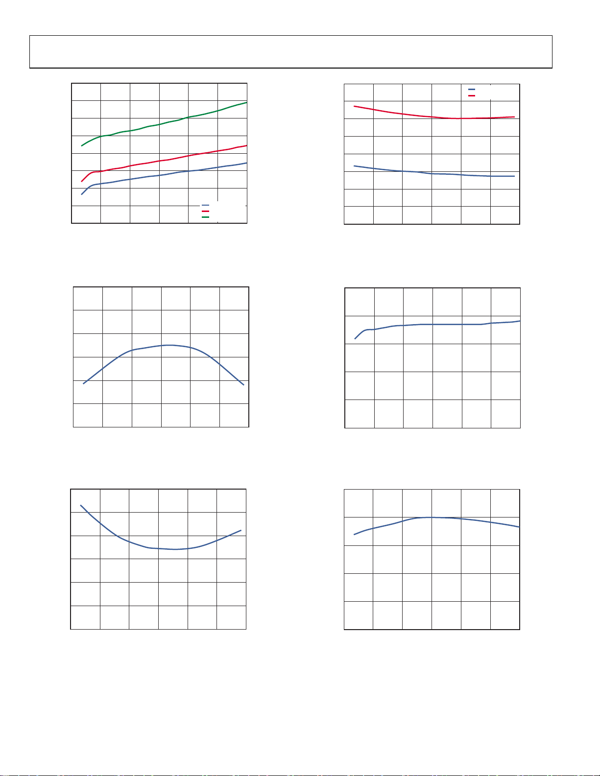
1600
1400
1200
Y (kHz)
1000
800
FREQUEN
600
400
–50 –20 10 40 70 100 130
08342-066
TEMPERATURE (°C)
f
SW
f
SW
= 1.4MHz
= 700kHz
08342-076
Figure 14. Frequency vs. Temperature
1600
1400
1200
Y (kHz)
1000
f
SW
f
SW
= 1.4MHz
= 700kHz
–0.05
LOAD REGUL
–0.10
–0.15
–0.20
0.20 0.4 0.6 0.8 1.0 1.2
Figure 12. Load Regulation, V
I
OUT
(A)
OUT
8342-067
= 3.3 V, VIN = 12 V
800
FREQUEN
600
400
2 5 8 11 14 17 20
V
(V)
IN
Figure 15. Frequency vs. VIN
08342-077
Rev. A | Page 7 of 28
ADP2300/ADP2301
40
35
160
140
f
SW
f
SW
= 1.4MHz
= 700kHz
30
25
20
15
10
SHUTDOWN CURRENT (µA)
5
0
2 5 8 11 14 17 20
VIN (V)
Figure 16. Shutdown Current vs. VIN
0.804
0.802
0.800
0.798
0.796
0.8V FEEDBACK VO LTAGE (V)
0.794
T
= −40°C
J
T
= +25°C
J
T
= +125°C
J
120
100
80
60
MINIMUM OFF TIME (ns)
40
20
0
–50 –20 10 40 70 100 130
8342-078
TEMPERATURE (°C)
08342-081
Figure 19. Minimum Off Time vs. Temperature
2.5
2.0
1.5
1.0
CURRENT LIMIT (A)
0.5
0.792
–50 –20 10 40 70 100 130
TEMPERATURE (°C)
Figure 17. 0.8 V Feedback Voltage vs. Temperature
110
105
100
95
90
MINIMUM ON TIME (ns)
85
80
–50 –20 10 40 70 100 130
TEMPERATURE (°C)
Figure 18. Minimum On Time vs. Temperature
0
2 5 8 11 14 17 20
08342-079
Figure 20. Current-Limit Threshold vs. VIN, V
2.5
2.0
1.5
1.0
CURRENT LIMIT (A)
0.5
0
–50 –20 10 40 70 100 130
08342-080
VIN (V)
TEMPERATURE (°C)
BST − VSW
= 5.0 V
08342-082
08342-083
Figure 21. Current-Limit Threshold vs. Temperature
Rev. A | Page 8 of 28
ADP2300/ADP2301
m
700
660
620
580
QUIESCENT CURRENT (µA)
540
500
25811141720
V
(V)
IN
TJ = −40°C
T
= +25°C
J
T
= +125°C
J
Figure 22. Quiescent Current vs. VIN
900
800
700
Ω)
600
(
500
DS (ON)
400
300
MOSFET R
200
100
0
–50 –20 10 40 70 100 130
TEMPERATURE (°C)
Figure 23. MOSFET R
vs. Temperature (Pin-to-Pin Measurements)
DS(ON)
VGS = 5V
V
GS
V
GS
= 4V
= 3V
08342-084
08342-085
3.0
2.9
2.8
2.7
2.6
2.5
2.4
2.3
UVLO THRESHO LD (V)
2.2
2.1
2.0
–50 –20 10 40 70 100 130
TEMPERATURE (°C)
Figure 25. UVLO Threshold vs. Temperature
V
OUT
1
4
2
CH1 5mV
B
CH2 5V M400ns A CH2 7.4V
W
CH4 500mA Ω
Figure 26. Steady State at Heavy Load, f
IL
SW
B
W
B
W
= 1.4 MHz, I
SW
RISING
FALLING
= 1 A
OUT
08342-087
08342-024
1.30
1.25
RISING
FALLING
V
1
OUT
1.20
1.15
4
IL
1.10
ENABLE THRESHOLD (V)
1.05
1.00
–50 –20 10 40 70 100 130
TEMPERATURE (°C)
Figure 24. Enable Threshold vs. Temperature
2
CH1 20mV
08342-086
B
CH2 5V M10µs A CH2 8V
W
CH4 200mA Ω
Figure 27. Steady State at Light Load, fSW = 1.4 MHz, I
SW
B
W
B
W
OUT
= 40 mA
8342-025
Rev. A | Page 9 of 28

ADP2300/ADP2301
V
OUT
IL
1
4
EN
SW
3
2
CH1 1V
CH3 10V
B
CH2 10V M100µ s A CH3 8V
W
B
CH4 500mA Ω
W
B
W
B
W
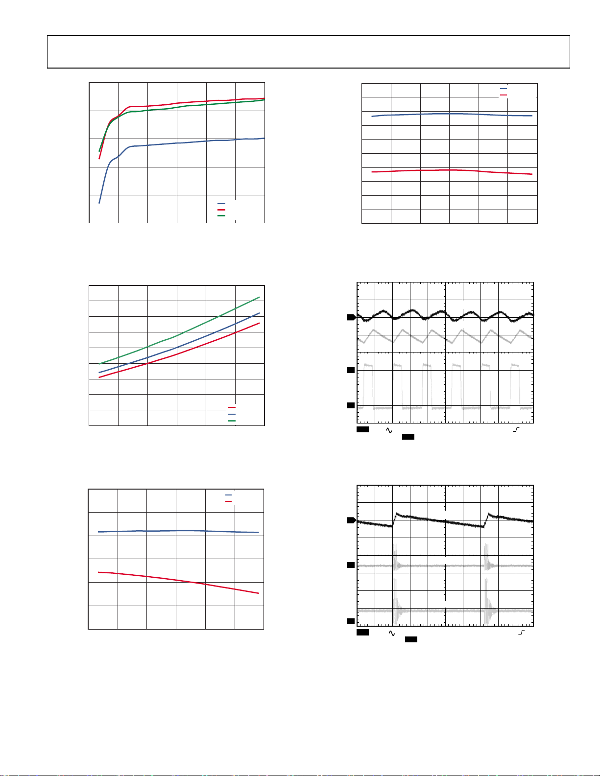
Figure 28. Soft Start with 1 A Resistance Load, fSW = 1.4 MHz
V
OUT
1
4
IL
EN
SW
3
2
CH1 1V
CH3 10V
B
CH2 10V M100µ s A CH3 8V
W
B
CH4 500mA Ω
W
B
W
B
W
Figure 29. Soft Start with No Load, fSW = 1.4 MHz
V
1
4
2
08342-026
CH1 50mV
B
CH2 10V M100 µs A CH4 630mA
W
CH4 500mA Ω
B
W
B
W
Figure 31. ADP2301 Load Transient, 0.2 A to 1.0 A, V
= 1.4 MHz, L = 4.7 μH, C
(f
SW
1
4
2
08342-027
CH1 200mV
B
CH2 10V M100 µs A CH4 630mA
W
CH4 500mA Ω
= 22 μF)
OUT
B
W
B
W
Figure 32. ADP2300 Load Transient, 0.2 A to 1.0 A, V
= 700 kHz, L = 10 μH, C
(f
SW
= 22 μF)
OUT
OUT
I
OUT
SW
= 3.3 V, VIN = 12 V
OUT
V
OUT
I
OUT
SW
= 5.0 V, VIN = 12 V
OUT
08342-058
08342-059
V
1
4
2
CH1 100mV
OUT
I
OUT
SW
B
CH2 10V M100µs A CH4 580mA
W
CH4 500mA Ω
B
W
B
W
Figure 30. ADP2301 Load Transient, 0.2 A to 1.0 A, V
= 1.4 MHz, L = 4.7 μH, C
(f
SW
= 10 μF)
OUT
= 5.0 V, VIN = 12 V
OUT
08342-057
Rev. A | Page 10 of 28
1
4
2
CH1 100mV
B
CH2 10V M100µ s A CH4 630mA
W
CH4 500mA Ω
B
W
B
W
Figure 33. ADP2300 Load Transient, 0.2 A to 1.0 A, V
= 700 kHz, L = 10 μH, C
(f
SW
= 22 μF)
OUT
V
OUT
I
OUT
SW
= 3.3 V, VIN = 12 V
OUT
08342-060

ADP2300/ADP2301
200
160
120
80
40
0
–40
–80
–120
–160
–200
PHASE [B/A] (Degrees)
1
3
2
CH1 5mV
CH3 5V
B
CH2 10V M1ms A CH3 11.4V
W
B
W
Figure 34. ADP2301 Line Transient,
7 V to 15 V, V
= 3.3 V, I
OUT
OUT
V
OUT
V
IN
SW
= 1.2 A, fSW = 1.4 MHz
100
80
60
40
20
0
–20
–40
MAGNITUDE [B/A] (dB)
–60
–80
CROSS FREQ UENCY: 127kHz
PHASE MARGIN: 53 °
–100
08342-061
1k 10k 100k
FREQUENCY (Hz)
Figure 37. ADP2301 Bode Plot, V
= 1.4 MHz, L = 4.7 μH, C
(f
SW
12
= 5.0 V, VIN = 12 V
OUT
OUT
1M
= 10 μF)
08342-062
V
OUT
1
IL
4
2
CH1 1V
B
CH2 10V M10µs A CH1 2.56V
W
CH4 1A Ω
SW
B
W
B
W
Figure 35. ADP2301 Short-Circuit Entry, V
= 1.4 MHz)
(f
SW
1
V
OUT
IL
4
2
CH1 1V
B
W
SW
CH2 10V M100 µs A CH1 1.2V
CH4 1A Ω
B
W
B
W
Figure 36. ADP2301 Short-Circuit Recovery, V
= 1.4 MHz)
(f
SW
= 3.3 V
OUT
OUT
= 3.3 V
100
80
60
40
20
0
–20
–40
MAGNITUDE [B/ A] (dB)
–60
–80
CROSS FREQ UENCY: 80kHz
PHASE MARGIN: 68°
–100
8342-033
1k 10k 100k
FREQUENCY (Hz)
Figure 38. ADP2301 Bode Plot, V
= 1.4 MHz, L = 4.7 μH, C
(f
SW
1
OUT
2
1M
= 3.3 V, VIN = 12 V
= 22 μF)
OUT
100
80
60
40
20
0
–20
–40
MAGNITUDE [B/A] (dB)
–60
–80
CROSS FREQ UENCY: 27kHz
PHASE MARGIN: 76°
–100
08342-034
1k 10k 100k
Figure 39. ADP2300 Bode Plot, V
(f
SW
12
1M
FREQUENCY (Hz)
= 5.0 V, VIN = 12 V
= 700 kHz, L = 10 μH, C
OUT
OUT
= 22 μF)
200
160
120
80
40
0
–40
–80
–120
–160
–200
200
160
120
80
40
0
–40
–80
–120
–160
–200
PHASE [B/A] ( Degrees)
08342-063
PHASE [B/A] (Degrees)
08342-064
Rev. A | Page 11 of 28

ADP2300/ADP2301
100
80
60
40
20
0
–20
–40
MAGNITUDE [B/A] (dB)
–60
–80
CROSS FREQUENCY: 47kHz
PHASE MARGIN: 77°
–100
1k 10k 100k
Figure 40. ADP2300 Bode Plot, V
= 700 kHz, L = 10 μH, C
(f
SW
12
FREQUENCY (Hz)
= 3.3 V, VIN = 12 V
OUT
OUT
1M
= 22 μF)
200
160
120
80
40
0
–40
–80
–120
–160
–200
PHASE [B/A] (Degrees)
08342-065
Rev. A | Page 12 of 28

ADP2300/ADP2301
V
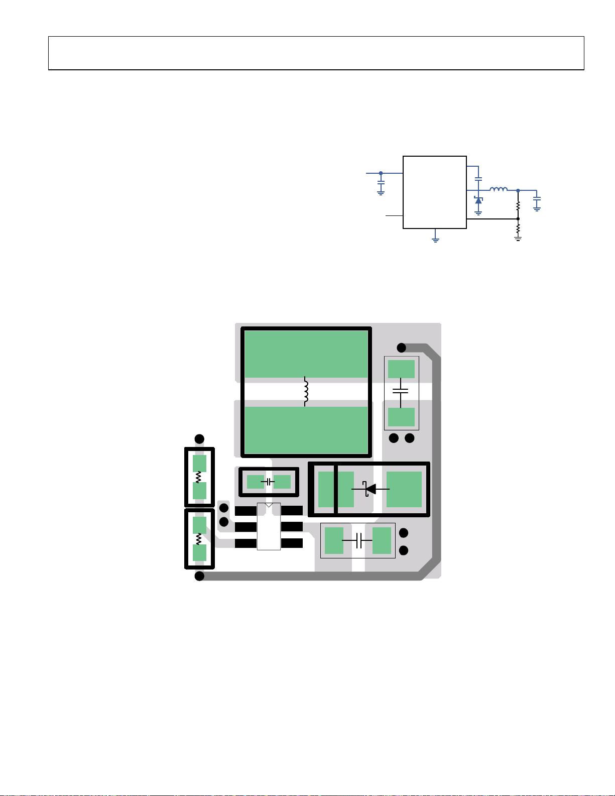
FUNCTIONAL BLOCK DIAGRAM
IN
VIN
5
OFF
ON
EN
FB
SHUTDOWN
4
3
THERMAL
1.20V
1.2µA
0.90V
0.8V
SHUTDOWN
OVP
220kΩ
90pF
LOGIC
SHUTDOWN IC
0.5V
V
= 1.1V
BIAS
0.7pF
UVLO
OCP
250mV/A
RAMP
GENERATOR
V
FB
BOOT
REGULATOR
RSQ
CLK
GENERATOR
FREQUENCY F OLDBACK
(
f
, ½
f
, ¼
f
SW
)
SW
SW
BST
1
V
OUT
SW
6
GND
2
ADP2300/ADP2301
08342-038
Figure 41. ADP2300/ADP2301 Functional Block Diagram
Rev. A | Page 13 of 28

ADP2300/ADP2301
THEORY OF OPERATION
The ADP2300/ADP2301 are nonsynchronous, step-down
dc-to-dc regulators, each with an integrated high-side power
MOSFET. A high switching frequency and ultrasmall, 6-lead
TSOT package allow small step-down dc-to-dc regulator
solutions.
The ADP2300/ADP2301 can operate with an input voltage from
3.0 V to 20 V while regulating an output voltage down to 0.8 V.
The ADP2300/ADP2301 are available in two fixed-frequency
options: 700 kHz (ADP2300) and 1.4 MHz (ADP2301).
BASIC OPERATION
The ADP2300/ADP2301 use the fixed-frequency, peak currentmode PWM control architecture at medium to high loads, but
shift to a pulse-skip mode control scheme at light loads to reduce
the switching power losses and improve efficiency. When the
devices operate in fixed-frequency PWM mode, output regulation
is achieved by controlling the duty cycle of the integrated MOSFET.
When the devices operate in pulse-skip mode at light loads, the
output voltage is controlled in a hysteretic manner with higher
output ripple. In this mode of operation, the regulator periodically
stops switching for a few cycles, thus keeping the conversion
losses minimal to improve efficiency.
Since the pulse-skip mode comparator monitors the internal
compensation node, which represents the peak inductor current
information, the average pulse-skip load current threshold depends
on the input voltage (V
and the output capacitor.
Because the output voltage occasionally dips below regulation
and then recovers, the output voltage ripple in the power saving
mode is larger than the ripple in the PWM mode of operation.
), the output voltage (V
IN
), the inductor,
OUT
BOOTSTRAP CIRCUITRY
The ADP2300/ADP2301 each have an integrated boot regulator,
which requires that a 0.1 µF ceramic capacitor (X5R or X7R) be
placed between the BST and SW pins to provide the gate drive
voltage for the high-side MOSFET. There must be at least a 1.2 V
difference between the BST and SW pins to turn on the high-side
MOSFET. This voltage should not exceed 5.5 V in case the BST
pin is supplied with an external voltage source through a diode.
The ADP2300/ADP2301 generate a typical 5.0 V bootstrap voltage
for a gate drive circuit by differentially sensing and regulating the
voltage between the BST and SW pins. A diode integrated on the
chip blocks the reverse voltage between the VIN and BST pins
when the MOSFET switch is turned on.
PWM MODE
In PWM mode, the ADP2300/ADP2301 operate at a fixed
frequency, set by an internal oscillator. At the start of each
oscillator cycle, the MOSFET switch is turned on, sending a
positive voltage across the inductor. The inductor current
increases until the current-sense signal crosses the peak
inductor current threshold that turns off the MOSFET switch;
this threshold is set by the error amplifier output. During the
MOSFET off time, the inductor current declines through the
external diode until the next oscillator clock pulse starts a new
cycle. The ADP2300/ADP2301 regulate the output voltage by
adjusting the peak inductor current threshold.
POWER SAVING MODE
To achieve higher efficiency, the ADP2300/ADP2301 smoothly
transition to the pulse-skip mode when the output load decreases
below the pulse-skip current threshold. When the output voltage
dips below regulation, the ADP2300/ADP2301 enter PWM mode
for a few oscillator cycles until the voltage increases to within
regulation. During the idle time between bursts, the MOSFET
switch is turned off, and the output capacitor supplies all the
output current.
PRECISION ENABLE
The ADP2300/ADP2301 feature a precision enable circuit that
has a 1.2 V reference voltage with 100 mV hysteresis. When the
voltage at the EN pin is greater than 1.2 V, the part is enabled. If the
EN voltage falls below 1.1 V, the chip is disabled. The precision
enable threshold voltage allows the ADP2300/ADP2301 to be
easily sequenced from other input/output supplies. It can also be
used as programmable UVLO input by using a resistive divider.
An internal 1.2 µA pull-down current prevents errors if the EN pin
is floating.
INTEGRATED SOFT START
The ADP2300/ADP2301 include internal soft start circuitry
that ramps the output voltage in a controlled manner during
startup, thereby limiting the inrush current. The soft start time is
typically fixed at 1460 µs for the ADP2300 and at 730 µs for the
ADP2301.
CURRENT LIMIT
The ADP2300/ADP2301 include current-limit protection circuitry
to limit the amount of positive current flowing through the highside MOSFET switch. The positive current limit on the power
switch limits the amount of current that can flow from the input
to the output.
Rev. A | Page 14 of 28

ADP2300/ADP2301
SHORT-CIRCUIT PROTECTION
The ADP2300/ADP2301 include frequency foldback to prevent
output current runaway when there is a hard short on the output.
The switching frequency is reduced when the voltage at the FB pin
drops below a certain value, which allows more time for the
inductor current to decline, but increases the ripple current while
regulating the peak current. This results in a reduction in average
output current and prevents output current runaway. The correlation between the switching frequency and the FB pin voltage
is shown in Tabl e 5 .
Table 5. Correlation Between the Switching Frequency
and the FB Pin Voltage
FB Pin Voltage Switching Frequency
VFB ≥ 0.6 V fSW
0.6 V > VFB > 0.2 V ½ fSW
VFB ≤ 0.2 V ¼ fSW
When a hard short (VFB ≤ 0.2 V) is removed, a soft start cycle
is initiated to regulate the output back to its level during normal
operation, which helps to limit the inrush current and prevent
possible overshoot on the output voltage.
UNDERVOLTAGE LOCKOUT (UVLO)
The ADP2300/ADP2301 have fixed, internally set undervoltage
lockout circuitry. If the input voltage drops below 2.4 V, the
ADP2300/ADP2301 shut down and the MOSFET switch turns
off. After the voltage rises again above 2.8 V, the soft start
period is initiated, and the part is enabled.
THERMAL SHUTDOWN
If the ADP2300/ADP2301 junction temperature rises above 140°C,
the thermal shutdown circuit disables the chip. Extreme junction
temperature can be the result of high current operation, poor
circuit board design, or high ambient temperature. A 15°C
hysteresis is included so that when thermal shutdown occurs,
the ADP2300/ADP2301 do not return to operation until the onchip temperature drops below 125°C. After the devices recover
from thermal shutdown, a soft start is initiated.
CONTROL LOOP
The ADP2300/ADP2301 are internally compensated to minimize
external component count and cost. In addition, the built-in
slope compensation helps to prevent subharmonic oscillations
when the ADP2300/ADP2301 operate at a duty cycle greater
than or close to 50%.
Rev. A | Page 15 of 28

ADP2300/ADP2301
−+××
=
−+××−=
APPLICATIONS INFORMATION
PROGRAMMING THE OUTPUT VOLTAGE
The output voltage of the ADP2300/ADP2301 is externally set by
a resistive voltage divider from the output voltage to the FB pin,
as shown in Figure 42. Suggested resistor values for the typical
output voltage setting are listed in Ta bl e 6. The equation for the
output voltage setting is
⎛
V
OUT
⎜
1V800.0
⎜
⎝
where:
V
is the output voltage.
OUT
R
is the feedback resistor from V
FB1
R
is the feedback resistor from FB to GND.
FB2
ADP2300/
ADP2301
FB
Figure 42. Programming the Output Voltage Using a Resistive Voltage Divider
Table 6. Suggested Values for Resistive Voltage Divider
V
(V) R
OUT
(kΩ), ±1% R
FB1
1.2 4.99 10
1.8 12.7 10.2
2.5 21.5 10.2
3.3 31.6 10.2
5.0 52.3 10
⎞
R
1
FB
⎟
+×=
⎟
R
2
FB
⎠
to FB.
OUT
V
OUT
R
FB1
R
FB2
08342-039
(kΩ), ±1%
FB2
VOLTAGE CONVERSION LIMITATIONS
There are both lower and upper output voltage limitations for a
given input voltage due to the minimum on time, the minimum
off time, and the bootstrap dropout voltage.
The lower limit of the output voltage is constrained by the finite,
controllable minimum on time, which can be as high as 135 ns for
the worst case. By considering the variation of both the switching
frequency and the input voltage, the equation for the lower limit
of the output voltage is
VVVftV
)(
OUT
(min)
-
INSW
(max)(max)
ONMIN
where:
V
is the maximum input voltage.
IN(max)
f
is the maximum switching frequency for the worst case.
SW(max)
is the minimum controllable on time.
t
MIN-ON
V
is the diode forward drop.
D
The upper limit of the output voltage is constrained by the minimum controllable off time, which can be as high as 120 ns in
the ADP2301 for the worst case. By considering the variation of
both the switching frequency and the input voltage, the equation
for the upper limit of the output voltage is
OUT
(max)
OFFMIN
(min)(max)
INSW
-
where:
is the minimum input voltage.
V
IN(min)
is the maximum switching frequency for the worst case.
f
SW(max)
V
is the diode forward drop.
D
is the minimum controllable off time.
t
MIN-OFF
In addition, the bootstrap circuit limits the minimum input
voltage for the desired output due to internal dropout voltage.
To attain stable operation at light loads and ensure proper startup
for the prebias condition, the ADP2300/ADP2301 require the
voltage difference between the input voltage and the regulated
output voltage (or between the input voltage and the prebias
voltage) to be greater than 2.1 V for the worst case. If the voltage
difference is smaller, the bootstrap circuit relies on some minimum
load current to charge the boost capacitor for startup. Figure 43
shows the typical required minimum input voltage vs. load current
for the 3.3 V output voltage.
DD
VVVftV
)()1(
DD
Rev. A | Page 16 of 28

ADP2300/ADP2301
V
5.5
5.3
5.1
4.9
4.7
(V)
4.5
IN
4.3
4.1
MINIMUM
3.9
3.7
3.5
1 10 100 1k
FOR STARTUP
FOR RUNNING
LOAD CURRENT (mA)
V
OUT
f
SW
= 3.3V
= 1.4MHz
Figure 43. Minimum Input Voltage vs. Load Current
Based on three conversion limitations (the minimum on time,
the minimum off time, and the bootstrap dropout
voltage), Figure 44 shows the voltage conversion limitations.
22
17
(V)
12
IN
V
7
MAXIMUM INPUT FOR ADP2300
MAXIMUM INPUT FOR ADP2301
2
2 4 6 8 10 12 14 160
MINIMUM INPUT FOR ADP2300/ADP2301
V
(V)
OUT
08342-055
Figure 44. Voltage Conversion Limitations
LOW INPUT VOLTAGE CONSIDERATIONS
For low input voltage between 3 V and 5 V, the internal boot
regulator cannot provide enough 5.0 V bootstrap voltage due to
the internal dropout voltage. As a result, the increased MOSFET
R
reduces the available load current. To prevent this, add
DS(ON)
an external small-signal Schottky diode from a 5.0 V external
bootstrap bias voltage. Because the absolute maximum rating
between the BST and SW pins is 6.0 V, the bias voltage should
be less than 5.5 V. Figure 45 shows the application diagram for
the external bootstrap circuit.
3V ~ 5V
VIN
ADP2300/
ADP2301
BST
SW
SCHOTTKY DIO DE
5V BIAS
VOLTAGE
PROGRAMMING THE PRECISION ENABLE
Generally, the EN pin can be easily tied to the VIN pin so that the
device automatically starts up when the input power is applied.
However, the precision enable feature allows the ADP2300/
ADP2301 to be used as a programmable UVLO by connecting
a resistive voltage divider to V
configuration prevents the start-up problems that can occur
when V
ramps up slowly in soft start with a relatively high
IN
load current.
V
IN
R
EN1
R
EN2
Figure 46. Precision Enable Used as a Programmable UVLO
The precision enable feature also allows the ADP2300/ADP2301 to
be sequenced precisely by using a resistive voltage divider with
another dc-to-dc output supply, as shown in Figure 47.
OTHER DC-TO-DC
OUTPUT
Figure 47. Precision Enable Used as a Sequencing Control
from Another DC-to-DC Output
With a 1.2 µA pull-down current on the EN pin, the equation for
the start-up voltage in Figure 46 and Figure 47 is
V2.1
⎛
V
STARTUP
⎜
⎜
R
2
EN
⎝
where:
is the start-up voltage to enable the chip.
V
STARTUP
is the resistor from the dc source to EN.
R
EN1
R
is the resistor from EN to GND.
EN2
, as shown in Figure 46. This
IN
VIN
ADP2300/
ADP2301
EN
ADP2300/
ADP2301
R
EN1
⎞
+=
⎟
⎟
⎠
EN
R
EN2
+×
R
1
EN
8342-043
08342-044
V2.1A2.1
OFF
ON
EN
GND
FB
08342-042
Figure 45. External Bootstrap Circuit for Low Input Voltage Application
Rev. A | Page 17 of 28

ADP2300/ADP2301
Δ
INDUCTOR
The high switching frequency of the ADP2300/ADP2301 allows
the use of small inductors. For best performance, use inductor
values between 2 H and 10 H for ADP2301, and use inductor
values between 2 H and 22 H for ADP2300.
The peak-to-peak inductor current ripple is calculated using the
following equation:
I
RIPPLE
−
VV
IN
=Δ
×
fL
sw
OUT
⎛
)(
OUT
⎜
×
⎜
⎝
where:
is the switching frequency.
f
SW
L is the inductor value.
is the diode forward drop.
V
D
is the input voltage.
V
IN
V
is the output voltage.
OUT
Inductors of smaller values are usually smaller in size and less
expensive, but increase the ripple current and the output voltage
ripple. As a guideline, the inductor peak-to-peak current ripple
should typically be set to 30% of the maximum load current for
optimal transient response and efficiency. Therefore, the inductor
value is calculated using the following equation:
L
where I
()
−
VV
IN
=
3.0
LOAD(max)
OUT
LOAD
(max)
is the maximum load current.
⎛
OUT
⎜
×
⎜
××
fI
sw
⎝
⎞
+
VV
D
⎟
⎟
+
VV
DIN
⎠
⎞
+
VV
D
⎟
⎟
+
VV
DIN
⎠
The inductor peak current is calculated using the following
equation:
I
RIPPLE
PEAK
II
LOAD
+=
(max)
2
The minimum current rating of the inductor must be greater
than the inductor peak current. For ferrite core inductors with a
quick saturation characteristic, the inductor saturation current
rating should be higher than the switch current-limit threshold
to prevent the inductor from reaching its saturation point. Be
sure to validate the worst-case condition, in which there is a
shorted output, over the intended temperature range.
Inductor conduction losses are caused by the flow of current
through the inductor, which is associated with the internal dc
resistance (DCR). Larger sized inductors have smaller DCR and,
therefore, may reduce inductor conduction losses. However,
inductor core losses are also related to the core material and the
ac flux swing, which are affected by the peak-to-peak inductor ripple current. Because the ADP2300/ADP2301 are high
switching frequency regulators, shielded ferrite core materials
are recommended for their low core losses and low EMI. Some
recommended inductors are shown in Tab le 7 .
Table 7. Recommended Inductors
Dimensions
Vendor Value (μH) Part No. DCR (mΩ) I
SAT
(A)
L × W × H (mm)
Coilcraft 4.7 LPS6225-472MLC 65 3.1 6.0 × 6.0 × 2.4
6.8 LPS6225-682MLC 95 2.7 6.0 × 6.0 × 2.4
10 LPS6225-103MLC 105 2.1 6.0 × 6.0 × 2.4
Sumida 4.7 CDRH5D28RHPNP-4R7N 43 3.7 6.2 × 6.2 × 3.0
4.7 CDRH5D16NP-4R7N 64 2.15 5.8 × 5.8 × 1.8
6.8 CDRH5D28RHPNP-6R8N 61 3.1 6.2 × 6.2 × 3.0
6.8 CDRH5D16NP-6R8N 84 1.8 5.8 × 5.8 × 1.8
10 CDRH5D28RHPNP-100M 93 2.45 6.2 × 6.2 × 3.0
Cooper Bussmann 4.7 SD53-4R7-R 39 2.1 5.2 × 5.2 × 3.0
6.8 SD53-6R8-R 59 1.85 5.2 × 5.2 × 3.0
10 DR73-100-R 65 2.47 7.6 × 7.6 × 3.5
Toko 4.7 B1077AS-4R7N 34 2.6 7.6 × 7.6 × 4.0
6.8 B1077AS-6R8N 40 2.3 7.6 × 7.6 × 4.0
10 B1077AS-100M 58 1.8 7.6 × 7.6 × 4.0
TDK 4.7 VLC5045T-4R7M 34 3.3 5.0 × 5.0 × 4.5
6.8 VLC5045T-6R8M 46 2.7 5.0 × 5.0 × 4.5
10 VLC5045T-100M 66 2.1 5.0 × 5.0 × 4.5
Rev. A | Page 18 of 28

ADP2300/ADP2301
Δ
CATCH DIODE
The catch diode conducts the inductor current during the off
time of the internal MOSFET. The average current of the diode
in normal operation is, therefore, dependent on the duty cycle
of the regulator as well as the output load current.
I
where V
⎛
OUT
⎜
−=
1
AVGDIODE
⎜
⎝
is the diode forward drop.
D
⎞
+
VV
D
⎟
I
×
LOAD
⎟
+
VV
DIN
⎠
(max))(
The only reason to select a diode with a higher current rating than
necessary in normal operation is for the worst-case condition, in
which there is a shorted output. In this case, the diode current
increases up to the typical peak current-limit threshold. Be sure to
consult the diode data sheet to ensure that the diode can operate
well within the thermal and electrical limits.
The reverse breakdown voltage rating of the diode must be higher
than the highest input voltage and allow an appropriate margin
for the ringing that may be present on the SW node. A Schottky
diode is recommended for best efficiency because it has a low
forward voltage drop and fast switching speed. Tab l e 8 provides
a list of recommended Schottky diodes.
Table 8. Recommended Schottky Diodes
V
I
Vendor Part No.
RRM
(V)
AVG
(A)
ON Semiconductor MBRS230LT3 30 2
MBRS240LT3 40 2
Diodes Inc. B230A 30 2
B240A 40 2
Vishay SL23 30 2
SS24 40 2
INPUT CAPACITOR
The input capacitor must be able to support the maximum input
operating voltage and the maximum rms input current. The
maximum rms input current flowing through the input
capacitor is I
withstanding the rms input current for an application’s maximum load current using the following equation:
/2. Select an input capacitor capable of
LOAD(max)
OUTPUT CAPACITOR
The output capacitor selection affects both the output voltage ripple
and the loop dynamics of the regulator. The ADP2300/ADP2301
are designed to operate with small ceramic capacitors that have low
equivalent series resistance (ESR) and equivalent series inductance
(ESL) and are, therefore, easily able to meet stringent output voltage
ripple specifications.
When the regulator operates in forced continuous conduction
mode, the overall output voltage ripple is the sum of the voltage
spike caused by the output capacitor ESR plus the voltage ripple
caused by charging and discharging the output capacitor.
⎛
⎜
×Δ=Δ
RIPPLERIPPLE
⎜
⎝
1
sw
+
××
CfIV8
ESR
OUT
Capacitors with lower ESR are preferable to guarantee low
output voltage ripple, as shown in the following equation:
V
RIPPLE
ESR
≤
C
OUT
Δ
I
RIPPLE
Ceramic capacitors are manufactured with a variety of dielectrics,
each with different behavior over temperature and applied voltage.
X5R or X7R dielectrics are recommended for best performance,
due to their low ESR and small temperature coefficients. Y5V
and Z5U dielectrics are not recommended because of their poor
temperature and dc bias characteristics.
In general, most applications using the ADP2301 (1.4 MHz
switching frequency) require a minimum output capacitor value
of 10 µF, whereas most applications using the ADP2300 (700 kHz
switching frequency) require a minimum output capacitor value
of 20 µF. Some recommended output capacitors for V
are listed in Ta ble 9 .
Table 9. Recommended Capacitors for V
Vendor Value Part No.
Murata 10 μF, 6.3 V GRM31MR60J106KE19 3.2 × 1.6 × 1.15
22 μF, 6.3 V GRM31CR60J226KE19 3.2 × 1.6 × 1.6
TDK 10 μF, 6.3 V C3216X5R0J106K 3.2 × 1.6 × 1.6
22 μF, 6.3 V C3216X5R0J226M 3.2 × 1.6 × 0.85
OUT
⎞
⎟
C
OUT
⎟
⎠
≤ 5.0 V
OUT
≤ 5.0 V
Dimensions
L × W × H (mm)
)1(
DDII
(max))(
LOADRMSIN
−××=
where D is the duty cycle and is equal to
VV
+
D
OUT
D
=
VV
+
DIN
The recommended input capacitor is ceramic with X5R or X7R
dielectrics due to its low ESR and small temperature coefficients.
A capacitance of 10 µF should be adequate for most applications.
To minimize supply noise, place the input capacitor as close to
the VIN pin of the ADP2300/ADP2301 as possible.
Rev. A | Page 19 of 28

ADP2300/ADP2301
THERMAL CONSIDERATIONS
The ADP2300/ADP2301 store the value of the inductor current
only during the on time of the internal MOSFET. Therefore, a small
amount of power is dissipated inside the ADP2300/ADP2301
package, which reduces thermal constraints.
However, when the application is operating under maximum
load with high ambient temperature and high duty cycle, the
heat dissipated within the package may cause the junction
temperature of the die to exceed the maximum junction
temperature of 125°C. If the junction temperature exceeds
140°C, the regulator goes into thermal shutdown and recovers
when the junction temperature drops below 125°C.
The junction temperature of the die is the sum of the ambient
temperature of the environment and the temperature rise of the
package due to power dissipation, as indicated in the following
equation:
= TA + TR
T
J
where:
is the junction temperature.
T
J
is the ambient temperature.
T
A
is the rise in temperature of the package due to power
T
R
dissipation.
The rise in temperature of the package is directly proportional
to the power dissipation in the package. The proportionality
constant for this relationship is the thermal resistance from the
junction of the die to the ambient temperature, as shown in the
following equation:
= θJA × PD
T
R
where:
is the rise in temperature of the package.
T
R
is the thermal resistance from the junction of the die to the
θ
JA
ambient temperature of the package.
is the power dissipation in the package.
P
D
Rev. A | Page 20 of 28

ADP2300/ADP2301
(
DESIGN EXAMPLE
This section provides the procedures to select the external components, based on the example specifications listed in Tab le 1 0 .
The schematic for this design example is shown in Figure 48.
Table 10. Step-Down DC-to-DC Regulator Requirements
Additional
Parameter Specification
Requirements
Input Voltage, VIN 12.0 V ± 10% None
Output Voltage, V
3.3 V, 1.2 A, 1% V
OUT
OUT
None
ripple at CCM mode
Programmable
UVLO Voltage
VIN start-up voltage
approximately 7.8 V
None
SWITCHING FREQUENCY SELECTION
Select the switching frequency—700 kHz (ADP2300) or 1.4 MHz
(ADP2301)—using the conversion limitation curve shown
in Figure 44 to assess the conversion limitations (the minimum o
n
time, the minimum off time, and the bootstrap dropout voltage).
For example, in Figure 44 V
= 12 V ± 10% is within the conver-
IN
sion limitation for both the 700 kHz and 1.4 MHz switching
frequencies for an output voltage of 3.3 V, but choosing the 1.4 MHz
switching frequency provides the smallest sized solution. If higher
efficiency is required, choose the 700 kHz option; however, the
PCB footprint area of the regulator will be larger because of the
bigger inductor and output capacitors.
CATCH DIODE SELECTION
Select the catch diode. A Schottky diode is recommended for best
efficiency because it has a low forward voltage drop and faster
switching speed. The average current of the catch diode in
normal operation, with a typical Schottky diode forward
voltage, can be calculated using the following equation:
VV⎞⎛+
D
OUT
⎜
I ×
1
AVGDIODE
−=
⎜
⎝
where:
= 3.3 V.
V
OUT
= 12 V.
V
IN
LOAD(max)
= 0.4 V.
D
= 1.2 A.
DIODE(AVG)
= 0.85 A.
I
V
Therefore, I
However, for the worst-case condition, in which there is a shorted
output, the diode current would be increased to 2 A typical, determined by the peak switch current limit (see Tabl e 1). In this case,
selecting a B230A, 2.0 A/30 V surface-mount Schottky diode
would result in more reliable operation.
⎟
I
LOAD
⎟
VV
+
DIN
⎠
(max))(
INDUCTOR SELECTION
Select the inductor by using the following equation:
⎛
)
−
VV
IN
LOAD
OUT
(max)
××
fI
=
L
3.0
OUT
⎜
×
⎜
sw
⎝
⎞
+
VV
D
⎟
⎟
+
VV
DIN
⎠
where:
V
= 3.3 V.
OUT
= 12 V.
V
IN
I
V
f
= 1.2 A.
LOAD(max)
= 0.4 V.
D
= 1.4 MHz.
SW
This results in L = 5.15 µH. The closest standard value is 4.7 µH;
therefore, I
RIPPLE
= 0.394 A.
The inductor peak current is calculated using the following
equation:
PEAK
LOAD
(max)
+=
2
IIIΔ
RIPPLE
where:
LOAD(max)
RIPPLE
= 1.2 A.
= 0.394 A.
I
I
Therefore, the calculated peak current for the inductor is 1.397 A.
However, to protect the inductor from reaching its saturation
point in the current-limit condition, the inductor should be rated
for at least a 2.0 A saturation current for reliable operation.
OUTPUT CAPACITOR SELECTION
Select the output capacitor based on the output voltage ripple
requirement, according to the following equation:
⎛
⎜
×Δ=Δ
RIPPLERIPPLE
⎜
⎝
1
sw
+
××
CfIV8
ESR
OUT
where:
= 0.394 A.
ΔI
RIPPLE
= 1.4 MHz.
f
SW
= 33 mV.
V
RIPPLE
If the ESR of the ceramic capacitor is 3 m, then C
Because the output capacitor is one of the two external components
that control the loop stability, most applications using the ADP2301
(1.4 MHz switching frequency) require a minimum 10 µF capacitance to ensure stability. According to the recommended external
components in Table 1 1, choose 22 µF with a 6.3 V voltage rating
for this example.
C
OUT
⎞
⎟
⎟
⎠
= 1.2 µF.
OUT
Rev. A | Page 21 of 28

ADP2300/ADP2301
RESISTIVE VOLTAGE DIVIDER SELECTION
To select the appropriate resistive voltage divider, first calculate the
output feedback resistive voltage divider, and then calculate the
resistive voltage divider for the programmable V
The output feedback resistive voltage divider is
⎛
V
OUT
⎜
1V800.0
⎜
⎝
For the 3.3 V output voltage, choose R
⎞
R
1
FB
⎟
+×=
⎟
R
2
FB
⎠
FB1
= 10.2 k as the feedback resistive voltage divider, according to
the recommended values in Tab le 1 1 .
start-up voltage.
IN
= 31.6 k and R
FB2
The resistive voltage divider for the programmable V
voltage is
V2.1
⎛
⎜
V
STARTUP
If V
R
EN1
= 7.8 V, choose R
STARTUP
, which in this case is 56 k.
+=
⎜
R
2
EN
⎝
⎞
⎟
⎟
⎠
= 10.2 k, and then calculate
EN2
+×
R
1
EN
start-up
IN
V2.1A2.1
VIN = 12V
C1
10µF
25V
56kΩ
1%
10.2kΩ
1%
VIN
ADP2301
R3
R4
(1.4MHz)
EN
GND
BST
SW
FB
C3
0.1µF
6.3V
D1
B230A
L1
4.7µH
2.0A
31.6kΩ
1%
10.2kΩ
1%
V
= 3.3V
OUT
1.2A
C2
22µF
R1
R2
6.3V
08342-045
Figure 48. Schematic for the Design Example
Table 11. Recommended External Components for Typical Applications at 1.2 A Output Load
Part Number VIN (V) V
(V) I
OUT
(A) L (μH) C
OUT
(μF) R
OUT
(kΩ), ±1% R
FB1
(kΩ), ±1%
FB2
ADP2300 (700 kHz) 18 3.3 1.2 10 22 31.6 10.2
18 5.0 1.2 15 22 52.3 10
12 1.2 1.2 6.8 2 × 22 4.99 10
12 1.8 1.2 6.8 2 × 22 12.7 10.2
12 2.5 1.2 10 22 21.5 10.2
12 3.3 1.2 10 22 31.6 10.2
12 5.0 1.2 10 22 52.3 10
9 3.3 1.2 10 22 31.6 10.2
9 5.0 1.2 10 22 52.3 10
5 1.8 1.2 4.7 2 × 22 12.7 10.2
5 2.5 1.2 4.7 22 21.5 10.2
ADP2301 (1.4 MHz) 18 3.3 1.2 4.7 22 31.6 10.2
18 5.0 1.2 6.8 10 52.3 10
12 2.5 1.2 4.7 22 21.5 10.2
12 3.3 1.2 4.7 22 31.6 10.2
12 5.0 1.2 4.7 10 52.3 10
9 3.3 1.2 4.7 22 31.6 10.2
9 5.0 1.2 4.7 10 52.3 10
5 1.8 1.2 2.2 2 × 22 12.7 10.2
5 2.5 1.2 2.2 22 21.5 10.2
Rev. A | Page 22 of 28
ADP2300/ADP2301
CIRCUIT BOARD LAYOUT RECOMMENDATIONS
Good circuit board layout is essential to obtain the best
performance from the ADP2300/ADP2301. Poor layout can
affect the regulation and stability, as well as the electromagnetic
interface (EMI) and electromagnetic compatibility (EMC)
performance. A PCB layout example is shown in Figure 50.
Refer to the following guidelines for a good PCB layout:
• Place the input capacitor, inductor, catch diode, output
capacitor, and bootstrap capacitor close to the IC using
short traces.
• Ensure that the high current loop traces are as short and wide
as possible. The high current path is shown in Figure 49.
• Maximize the size of ground metal on the component side
to improve thermal dissipation.
• Use a ground plane with several vias connecting to the
component side ground to further reduce noise interference on sensitive circuit nodes.
INDUC TOR
L1
• Minimize the length of the FB trace connecting the top of the
feedback resistive voltage divider to the output. In addition,
keep these traces away from the high current traces and the
switch node to avoid noise pickup.
GND
BST
SW
FB
08342-046
VIN
ADP2300/
ADP2301
EN
Figure 49. Typical Application Circuit with High Current Traces Shown in Blue
C3
OUTPUT CAP
R
FB2
BST CAP
CATCH DIODE
D1
C1
C2
R
FB1
ADP2300/ADP2301
Figure 50. Recommended PCB Layout for the ADP2300/ADP2301
INPUT CAP
08342-056
Rev. A | Page 23 of 28

ADP2300/ADP2301
TYPICAL APPLICATION CIRCUITS
VIN = 12V
C1
10µF
25V
OFF
100kΩ
5%
ON
R3
VIN
EN
ADP2300
(700kHz)
GND
Figure 51. ADP2300—700 kHz Typical Application, V
BST
SW
FB
= 12 V, V
IN
C4
0.1µF
L1
6.3V
6.8µH
2.0A
D1
B230A
OUT
R1
4.99kΩ
1%
R2
10kΩ
1%
= 1.2 V/1.2 A with External Enabling
V
OUT
C2
22µF
6.3V
= 1.2V
1.2A
C3
22µF
6.3V
8342-052
VIN = 12V
C1
10µF
25V
OFF
R3
100kΩ
5%
ON
VIN
EN
ADP2300
(700kHz)
GND
Figure 52. ADP2300—700 kHz Typical Application, V
BST
SW
FB
= 12 V, V
IN
C4
0.1µF
L1
6.3V
6.8µH
2.0A
D1
B230A
12.7kΩ
10.2kΩ
= 1.8 V/1.2 A with External Enabling
OUT
1%
1%
R2
V
OUT
1.2A
C2
22µF
6.3V
R1
= 1.8V
C3
22µF
6.3V
8342-051
VIN = 12V
C1
10µF
25V
OFF
R3
100kΩ
5%
ON
VIN
EN
ADP2300
(700kHz)
GND
Figure 53. ADP2300—700 kHz Typical Application, V
BST
SW
FB
= 12 V, V
IN
C3
L1
0.1µF
10µH
6.3V
2.0A
D1
B230A
21.5kΩ
10.2kΩ
= 2.5 V/1.2 A with External Enabling
OUT
R1
1%
R2
1%
= 2.5V
V
OUT
1.2A
C2
22µF
6.3V
8342-050
Rev. A | Page 24 of 28

ADP2300/ADP2301
VIN= 12V
C1
10µF
25V
56kΩ
1%
10.2kΩ
1%
R3
R4
VIN
EN
ADP2301
(1.4MHz)
GND
Figure 54. ADP2301—1.4 MHz Typical Application, V
(with Programmable 7.8 V Start-Up Input Voltage)
BST
SW
FB
C3
0.1µF
6.3V
D1
B230A
L1
4.7µH
2.0A
= 12 V, V
IN
31.6kΩ
1%
10.2kΩ
1%
OUT
R1
R2
V
= 3.3V
OUT
1.2A
= 3.3 V/1.2 A
C2
22µF
6.3V
08342-049
VIN = 12V
C1
10µF
25V
OFF
100kΩ
5%
ON
R3
VIN
EN
ADP2301
(1.4MHz)
GND
Figure 55. ADP2301—1.4 MHz Typical Application, V
VIN = 18V
C1
10µF
25V
OFF
100kΩ
5%
ON
R3
VIN
EN
ADP2301
(1.4MHz)
GND
Figure 56. ADP2301—1.4 MHz Typical Application, V
VIN = 9V
C1
10µF
25V
OFF
100kΩ
5%
ON
R3
VIN
EN
ADP2301
(1.4MHz)
GND
Figure 57. ADP2301—1.4 MHz Typical Application, V
BST
SW
FB
IN
BST
SW
FB
IN
BST
SW
FB
IN
C3
0.1µF
6.3V
= 12 V, V
= 18 V, V
= 9 V, V
L1
4.7µH
2.0A
D1
B230A
52.3kΩ
= 5.0 V/1.2 A with External Enabling
OUT
C3
L1
0.1µF
6.8µH
6.3V
2.0A
D1
B230A
= 5.0 V/1.2 A with External Enabling
OUT
C3
L1
0.1µF
4.7µH
6.3V
2.0A
D1
B230A
= 3.3 V/1.2 A with External Enabling
OUT
R1
1%
R2
10kΩ
1%
52.3kΩ
1%
10.2kΩ
1%
31.6kΩ
1%
10.2kΩ
1%
V
= 5V
OUT
1.2A
C2
10µF
6.3V
V
= 5.0V
OUT
1.2A
C2
R1
R2
R1
R2
10µF
6.3V
= 3.3V
V
OUT
1.2A
C2
22µF
6.3V
8342-048
08342-090
08342-091
VIN = 5V
C1
10µF
25V
R3
100kΩ
5%
ON
OFF
Figure 58. ADP2301—1.4 MHz Typical Application, V
VIN
EN
ADP2301
(1.4MHz)
GND
BST
SW
FB
= 5 V, V
IN
C4
0.1µF
6.3V
D1
B230A
Rev. A | Page 25 of 28
L1
2.2µH
2.0A
12.7kΩ
10.2kΩ
= 1.8 V/1.2 A with External Enabling
OUT
1%
1%
= 1.8V
V
OUT
1.2A
R1
R2
C2
22µF
6.3V
C3
22µF
6.3V
8342-092

ADP2300/ADP2301
C
C
OUTLINE DIMENSIONS
2.90 BS
1.90
BSC
45
2.80 BSC
2
0.95 BSC
*
1.00 MAX
SEATING
PLANE
0.20
0.08
8°
4°
0°
0.60
0.45
0.30
102808-A
1.60 BSC
INDI
*
0.87
0.84
0.10 MAX
PIN 1
ATO R
0.90
6
13
0.50
0.30
*
COMPLIANT TO JEDEC ST ANDARDS MO-193-AA WI TH
THE EXCEPTI ON OF PACKAG E HEIGHT AND T HICKNESS.
Figure 59. 6-Lead Thin Small Outline Transistor Package [TSOT]
(UJ-6)
Dimensions shown in millimeters
ORDERING GUIDE
Switching
Model1
Frequency
Temperature Range Package Description
ADP2300AUJZ-R7 700 kHz −40°C to +125°C 6-Lead Thin Small Outline Transistor Package [TSOT] UJ-6 L87
ADP2300-EVALZ Evaluation Board
ADP2301AUJZ-R7 1.4 MHz −40°C to +125°C 6-Lead Thin Small Outline Transistor Package [TSOT] UJ-6 L86
ADP2301-EVALZ Evaluation Board
1
Z = RoHS Compliant Part.
Package
Option
Branding
Rev. A | Page 26 of 28

ADP2300/ADP2301
NOTES
Rev. A | Page 27 of 28

ADP2300/ADP2301
NOTES
©2010 Analog Devices, Inc. All rights reserved. Trademarks and
registered trademarks are the property of their respective owners.
D08342-0-6/10(A)
Rev. A | Page 28 of 28
 Loading...